JP2017009355A - Signal level adjustment device, phase detection device, motor drive control device, transport device, and signal level adjustment method - Google Patents
Signal level adjustment device, phase detection device, motor drive control device, transport device, and signal level adjustment method Download PDFInfo
- Publication number
- JP2017009355A JP2017009355A JP2015123234A JP2015123234A JP2017009355A JP 2017009355 A JP2017009355 A JP 2017009355A JP 2015123234 A JP2015123234 A JP 2015123234A JP 2015123234 A JP2015123234 A JP 2015123234A JP 2017009355 A JP2017009355 A JP 2017009355A
- Authority
- JP
- Japan
- Prior art keywords
- level
- signal
- signal level
- level adjustment
- input signal
- Prior art date
- Legal status (The legal status is an assumption and is not a legal conclusion. Google has not performed a legal analysis and makes no representation as to the accuracy of the status listed.)
- Pending
Links
Images



Classifications
-
- G—PHYSICS
- G03—PHOTOGRAPHY; CINEMATOGRAPHY; ANALOGOUS TECHNIQUES USING WAVES OTHER THAN OPTICAL WAVES; ELECTROGRAPHY; HOLOGRAPHY
- G03G—ELECTROGRAPHY; ELECTROPHOTOGRAPHY; MAGNETOGRAPHY
- G03G15/00—Apparatus for electrographic processes using a charge pattern
- G03G15/50—Machine control of apparatus for electrographic processes using a charge pattern, e.g. regulating differents parts of the machine, multimode copiers, microprocessor control
- G03G15/5008—Driving control for rotary photosensitive medium, e.g. speed control, stop position control
-
- H—ELECTRICITY
- H04—ELECTRIC COMMUNICATION TECHNIQUE
- H04B—TRANSMISSION
- H04B15/00—Suppression or limitation of noise or interference
- H04B15/02—Reducing interference from electric apparatus by means located at or near the interfering apparatus
- H04B15/04—Reducing interference from electric apparatus by means located at or near the interfering apparatus the interference being caused by substantially sinusoidal oscillations, e.g. in a receiver or in a tape-recorder
Landscapes
- Engineering & Computer Science (AREA)
- Microelectronics & Electronic Packaging (AREA)
- Physics & Mathematics (AREA)
- General Physics & Mathematics (AREA)
- Computer Networks & Wireless Communication (AREA)
- Signal Processing (AREA)
- Control Of Motors That Do Not Use Commutators (AREA)
- Transmission And Conversion Of Sensor Element Output (AREA)
Abstract
【課題】モータの回転位相検出精度を上げる信号レベル調整装置を提供する。
【解決手段】信号レベル調整装置10が、正弦波若しくは正弦波に準じた入力信号のピークレベル及びボトムレベルをそれぞれ検出し、検出手段が検出した入力信号の複数回のピークレベル及びボトムレベルに基づいて、入力信号の所定区間でレベル調整を行う。
【選択図】図1A signal level adjusting device for improving the rotational phase detection accuracy of a motor is provided.
A signal level adjusting device detects a peak level and a bottom level of an input signal according to a sine wave or a sine wave, respectively, and based on a plurality of peak levels and a bottom level of the input signal detected by the detecting means. Then, level adjustment is performed in a predetermined section of the input signal.
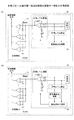
[Selection] Figure 1
Description
本発明は、信号レベル調整装置、位相検出装置、モータ駆動制御装置、搬送装置及び信号レベル調整方法に関する。 The present invention relates to a signal level adjustment device, a phase detection device, a motor drive control device, a transport device, and a signal level adjustment method.
従来、DCモータの制御において、回転子の回転位置の検出を行う技術が知られている。 Conventionally, a technique for detecting the rotational position of a rotor in the control of a DC motor is known.
特許文献1では、回転位相に応じて出力される複数のセンサ信号を用いて、このセンサ信号のレベルが所望の回転位相に応じた閾値に達した場合と、センサのゼロクロス点に達した場合とに回転位置を検出する技術が知られている(例えば、特許文献1等)。
In
しかしながら、特許文献1の技術では、製造過程の取り付け位相誤差又は着磁ばらつきによる位相誤差が検出位相の誤差になるおそれがある。
However, in the technique of
本発明は、上記課題に鑑みてなされたものであり、モータの回転位相検出精度を上げることができる信号レベル調整装置を提供することを目的とする。 The present invention has been made in view of the above problems, and an object of the present invention is to provide a signal level adjusting device capable of increasing the rotational phase detection accuracy of a motor.
一態様における、信号レベル調整装置は、正弦波若しくは正弦波に準じた入力信号のピークレベル及びボトムレベルをそれぞれ検出する検出手段と、前記検出手段が検出した前記入力信号の複数回のピークレベル及びボトムレベルに基づいて、前記入力信号の所定区間でレベル調整を行うレベル調整手段とを備える。 In one aspect, the signal level adjusting device includes a detection unit that detects a sine wave or a peak level and a bottom level of the input signal according to the sine wave, and a plurality of peak levels of the input signal detected by the detection unit, Level adjustment means for performing level adjustment in a predetermined section of the input signal based on the bottom level.
本発明の各実施形態によれば、モータの回転位相検出精度を上げることができる信号レベル調整装置を提供することができる。 According to each embodiment of the present invention, it is possible to provide a signal level adjusting device capable of increasing the rotational phase detection accuracy of a motor.
以下、本発明の実施形態について添付の図面を参照しながら説明する。なお、本明細書及び図面において、実質的に同一の機能構成を有する構成要素については、同一の符号を付し、重複した説明を省く。 Hereinafter, embodiments of the present invention will be described with reference to the accompanying drawings. In the present specification and drawings, components having substantially the same functional configuration are denoted by the same reference numerals, and redundant description is omitted.
[第1実施形態]
<信号レベル調整装置例>
はじめに、本実施形態に係る信号レベル調整装置の一例について説明する。
[First Embodiment]
<Example of signal level adjustment device>
First, an example of the signal level adjusting device according to the present embodiment will be described.
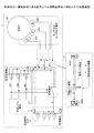
図1は、本発明の一実施形態に係る信号レベル調整装置の一例を示す全体構成図である。図1において、本実施形態に係るモータ駆動制御装置1は、モータM1を有する。また、モータM1は、回転子を有し、回転子の周囲には、回転子の回転角を検出するため、複数の磁気センサ(以下単に「センサ」という。)SR1乃至SR3(U相、V相及びW相)がそれぞれ設置される。各センサSR1乃至SR3は、複数のコイルを有するモータM1が持つ回転子の磁束密度の変化に応じて、連続的に変化する複数の信号に基づいて位相を示すセンサ信号をそれぞれ出力する。
FIG. 1 is an overall configuration diagram showing an example of a signal level adjusting apparatus according to an embodiment of the present invention. In FIG. 1, a motor
各センサSR1乃至SR3には、例えば、ホール素子等が使用される。ホール素子が使用される各センサSR1乃至SR3から出力されるそれぞれのセンサ信号は、正弦波又は正弦波に準じた波形の信号となる。また、モータM1がブラシレスDCモータであるとすると、各センサSR1乃至SR3は、例えば、電気角が120degとなる間隔でそれぞれ設置される。なお、ホール素子による出力については、後述する。 For each sensor SR1 to SR3, for example, a Hall element or the like is used. Each sensor signal output from each of the sensors SR1 to SR3 in which the Hall element is used is a sine wave or a signal having a waveform according to the sine wave. Also, assuming that the motor M1 is a brushless DC motor, the sensors SR1 to SR3 are respectively installed at intervals at which the electrical angle is 120 degrees, for example. The output by the Hall element will be described later.
モータ駆動制御装置1は、信号レベル調整装置10を有し、信号レベル調整装置10は、モータ駆動制御装置1は、例えば、図示するように、それぞれ接続される。この例では、信号レベル調整装置10は、各センサSR1乃至SR3が出力するそれぞれのセンサ信号を入力信号として入力する。即ち、入力信号は、例えば、正弦波SIG1である。なお、入力信号は、正弦波SIG1に、正弦波SIG1より低周波な成分が含まれる正弦波等の正弦波に準じた信号でもよい。以下、入力信号が、正弦波SIG1である例で説明する。また、入力信号は、センサ信号に含まれるノイズをローパスフィルタ等で減衰させた信号又はアンプで増幅させた信号等のセンサ加工信号でもよい。
The motor
入力信号に対して、信号レベル調整装置10は、調整等を行い、補正後正弦波SIG2を出力する。なお、補正後正弦波SIG2は、信号レベル調整装置10から出力信号U1、V1及びW1としてそれぞれ出力される。また、入力信号は、モータM1の動作に応じて定期的又は不定期に入力される。
The signal
さらに、モータ駆動制御装置1は、交点位相検出部を有し、交点位相検出部は、出力信号U1、V1及びW1の交点をそれぞれ検出する。なお、出力信号U1とV1との交点を示す信号を交点検出信号UVとする。同様に、出力信号V1とW1との交点を示す信号を交点検出信号VWとし、及び出力信号W1とU1との交点を示す信号を交点検出信号WUとする。
Furthermore, the motor
さらにまた、モータ駆動制御装置1は、信号選択部を有し、信号選択部は、交点検出信号UV、VW及びWUに基づいて、出力信号U1、V1及びW1のうち、いずれかを選択信号Xとする。次に、選択信号Xは、モータ駆動制御装置1が有する位相検出部に送信される。
Furthermore, the motor
位相検出部は、モータM1の回転位置に応じた複数の閾値を設定する。位相検出部に送信される選択信号Xが設定されるいずれかの閾値となると、位相検出部は、閾値となったこと等を示す位相情報を出力する。なお、位相検出部における信号BiasA及びBiasBは、交点レベル又は交点レベルに基づく信号である。 The phase detection unit sets a plurality of thresholds corresponding to the rotational position of the motor M1. When the selection signal X transmitted to the phase detection unit reaches any threshold value set, the phase detection unit outputs phase information indicating that the threshold value has been reached. Note that the signals BiasA and BiasB in the phase detection unit are signals based on the intersection level or the intersection level.
なお、信号レベル調整装置10及び図1に示す各部は、例えば、電子回路によって実現される。また、信号レベル調整装置10は、モータに係るセンサ信号以外を入力信号として入力してもよい。
Note that the signal
<検出及び調整例>
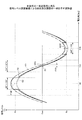
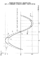
図2は、本発明の一実施形態に係る信号レベル調整装置による検出及び調整の一例を示す波形図である。図示するように、第1グラフG1は、信号レベル調整装置に入力される正弦波SIG1(図1)の1周期を示した例である。具体的には、第1グラフG1は、複数のセンサ信号、即ち、各センサの磁束密度の変化に応じた信号同士の交点となる信号レベルを示す。一方、図2は、理想的な正弦波の例を第2グラフG2で示す。例えば、あるセンサを基準に電気角が30degとなる点で交差した場合には、その交点の信号レベルは、理想的な正弦波では、正弦波振幅の1/2倍、即ち、sin30deg倍となる。
<Example of detection and adjustment>
FIG. 2 is a waveform diagram showing an example of detection and adjustment by the signal level adjustment device according to the embodiment of the present invention. As shown in the figure, the first graph G1 is an example showing one cycle of the sine wave SIG1 (FIG. 1) input to the signal level adjusting device. Specifically, the first graph G1 shows a signal level that is an intersection of a plurality of sensor signals, that is, signals corresponding to changes in the magnetic flux density of each sensor. On the other hand, FIG. 2 shows an example of an ideal sine wave by a second graph G2. For example, when crossing at a point where the electrical angle is 30 deg with respect to a certain sensor, the signal level at the intersection is ½ times the amplitude of the sine wave, that is, sin 30 deg times for an ideal sine wave. .
また、図2では、コモンレベルComは、グラウンド(GND)の信号レベル又はグラウンドに対して所定の電位となるオフセットを有する信号レベルである。即ち、コモンレベルComと各センサ信号との交点が、ゼロクロス点ZCとなる。なお、オフセットは、あらかじめ設定される値等である。 In FIG. 2, the common level Com is a signal level of ground (GND) or a signal level having an offset that is a predetermined potential with respect to the ground. That is, the intersection of the common level Com and each sensor signal is the zero cross point ZC. The offset is a value set in advance.
信号レベル調整装置は、入力信号、即ち、第1グラフG1で示す信号を同相レベル調整して補正後正弦波SIG2(図1)を生成し、出力する。なお、図2は、補正後正弦波SIG2の例を第3グラフG3で示す。図示するように、信号レベル調整装置は、第1グラフG1に示す信号の信号レベルを検出し、検出される信号レベルに応じた低周波成分及びオフセット量をそれぞれ算出して調整を行う。即ち、信号レベル調整装置は、調整によって、「位相検出区間」等の所定区間において、低周波成分を除去し、位相を第2グラフG2で示す信号に近づける。 The signal level adjusting device adjusts the in-phase level of the input signal, that is, the signal indicated by the first graph G1, and generates and outputs a corrected sine wave SIG2 (FIG. 1). FIG. 2 shows a third graph G3 as an example of the corrected sine wave SIG2. As shown in the figure, the signal level adjusting device detects the signal level of the signal shown in the first graph G1, and calculates and adjusts the low frequency component and the offset amount corresponding to the detected signal level. That is, the signal level adjustment device removes the low frequency component in a predetermined section such as the “phase detection section” by the adjustment, and brings the phase closer to the signal indicated by the second graph G2.
具体的には、まず、信号レベル調整装置は、各周期の第1グラフG1において、ピークレベルをそれぞれ検出する。また、ピークレベルは、図示するように、電気角が90deg±30degとなる信号レベル検出区間、即ち、電気角が60deg乃至120degとなる区間において、最も信号レベルが高くなった信号レベルである。したがって、1回の周期で1つピークレベルが検出される。なお、平均ピークレベルPaは、各周期でそれぞれ検出される複数のピークレベルを平均又は移動平均して計算される信号レベルである。 Specifically, first, the signal level adjusting device detects a peak level in the first graph G1 of each period. As shown in the figure, the peak level is the signal level with the highest signal level in the signal level detection section where the electrical angle is 90 deg ± 30 deg, that is, in the section where the electrical angle is 60 deg to 120 deg. Therefore, one peak level is detected in one cycle. The average peak level Pa is a signal level calculated by averaging or moving average a plurality of peak levels detected in each cycle.
同様に、信号レベル調整装置は、各周期の第1グラフG1において、ボトムレベルをそれぞれ検出する。また、ボトムレベルは、図示するように、電気角が270deg±30degとなる信号検出区間、即ち、電気角が240deg乃至300degとなる区間において、最も信号レベルが低くなった信号レベルである。したがって、1回の周期で1つボトムレベルが検出される。なお、平均ボトムレベルBaは、各周期でそれぞれ検出される複数のボトムレベルを平均又は移動平均して計算される信号レベルである。 Similarly, the signal level adjusting device detects the bottom level in the first graph G1 of each period. Further, as shown in the figure, the bottom level is a signal level having the lowest signal level in a signal detection section where the electrical angle is 270 deg ± 30 deg, that is, a section where the electrical angle is 240 deg to 300 deg. Therefore, one bottom level is detected in one cycle. The average bottom level Ba is a signal level calculated by averaging or moving average a plurality of bottom levels detected in each cycle.
低周波成分は、例えば、平均ピークレベルPaと、各ピークレベルとの差分PDIFである。又は低周波成分は、平均ボトムレベルBaと、各ボトムレベルとの差分BDIFである。いずれかの低周波成分が演算されると、ゼロクロス点ZCにおける第1グラフG1と第2グラフG2とのオフセット量OFSが求まる。即ち、信号レベル調整装置は、まず、いずれかの低周波成分に基づいてゼロクロス点ZCにおけるオフセット量OFSを求める。次に、信号レベル調整装置は、求まるオフセット量OFSに基づいて、電気角が180deg±30degとなる「位相検出区間」、即ち、電気角が150deg乃至210degとなる区間において、同相レベルを調整する。同相レベルが調整されると、信号レベル調整装置は、ゼロクロス点ZCで、位相を第2グラフG2に近づけることができる。 The low frequency component is, for example, a difference PDIF between the average peak level Pa and each peak level. Alternatively, the low frequency component is a difference BDIF between the average bottom level Ba and each bottom level. When any of the low frequency components is calculated, an offset amount OFS between the first graph G1 and the second graph G2 at the zero cross point ZC is obtained. That is, the signal level adjusting device first obtains the offset amount OFS at the zero cross point ZC based on any low frequency component. Next, the signal level adjusting device adjusts the in-phase level in the “phase detection section” in which the electrical angle is 180 deg ± 30 deg, that is, the section in which the electrical angle is 150 deg to 210 deg, based on the obtained offset amount OFS. When the in-phase level is adjusted, the signal level adjusting device can bring the phase closer to the second graph G2 at the zero cross point ZC.
センサ信号には、磁束密度のばらつき、いわゆる着磁ばらつきがあると、ゼロクロス点において、位相誤差がある場合がある。図2では、ゼロクロス点ZCにおける第1グラフG1と、第2グラフG2との差が、位相誤差ERRの例である。これに対して、同相レベルが調整されると、ゼロクロス点ZCにおいて、位相が理想である第2グラフG2に近づくため、信号レベル調整装置は、位相誤差ERRを少なくすることができる。 If the sensor signal has a variation in magnetic flux density, so-called magnetization variation, there may be a phase error at the zero cross point. In FIG. 2, the difference between the first graph G1 and the second graph G2 at the zero cross point ZC is an example of the phase error ERR. On the other hand, when the in-phase level is adjusted, the signal level adjusting device can reduce the phase error ERR because the phase approaches the ideal second graph G2 at the zero cross point ZC.
また、あるセンサ信号と交差する信号との間に位相誤差が生じていた場合には、交点の信号レベルは、理想的な信号レベルから離れてしまう誤差、いわゆる取り付け位相誤差が生じる場合がある。これに対して、ゼロクロス点ZCにおいて、位相が理想である第2グラフG2に近づくと、信号レベル調整装置は、取り付け位相誤差を少なくすることができる。 In addition, when a phase error has occurred between a certain sensor signal and a signal that intersects, the signal level at the intersection may deviate from an ideal signal level, that is, a so-called attachment phase error may occur. On the other hand, when the phase approaches the ideal second graph G2 at the zero-cross point ZC, the signal level adjusting device can reduce the mounting phase error.
さらに、ゼロクロス点ZCにおいて、位相が理想である第2グラフG2に近づくと、信号レベル調整装置は、ゼロクロス点ZC以外の他の点でも、位相誤差が少なくできる。 Further, when approaching the second graph G2 where the phase is ideal at the zero cross point ZC, the signal level adjusting device can reduce the phase error at other points than the zero cross point ZC.
信号レベル調整装置は、位相誤差ERRを少なくすることができると、検出する位相の精度をよくでき、モータの回転位相検出精度を上げることができる。 If the signal level adjusting device can reduce the phase error ERR, the accuracy of the phase to be detected can be improved, and the rotational phase detection accuracy of the motor can be increased.
一方、ピークレベルが検出される電気角が60deg乃至120degとなる区間と、ボトムレベルが検出される電気角が240deg乃至300degとなる区間とでは、図示するように、第3グラフG3は、第1グラフG1となるようにされる。これは、第1グラフG1が有するピークレベル及びボトムレベルをそれぞれ検出するためである。 On the other hand, in the section where the electrical angle where the peak level is detected is 60 deg to 120 deg and the section where the electrical angle where the bottom level is detected is 240 deg to 300 deg. A graph G1 is obtained. This is for detecting the peak level and the bottom level of the first graph G1.
<全体処理例>
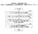
図3は、本発明の一実施形態に係る信号レベル調整装置による全体処理の一例を示すフローチャートである。
<Example of overall processing>
FIG. 3 is a flowchart illustrating an example of overall processing performed by the signal level adjustment apparatus according to the embodiment of the present invention.
ステップS01では、信号レベル調整装置は、ピークレベル及びボトムレベルをそれぞれ検出する。例えば、図2で図示するように、信号レベル調整装置は、電気角が90deg±30degとなる信号レベル検出区間では、ピークレベルを検出する。同様に、信号レベル調整装置は、電気角が270deg±30degとなる信号レベル検出区間では、ボトムレベルを検出する。 In step S01, the signal level adjusting device detects a peak level and a bottom level, respectively. For example, as illustrated in FIG. 2, the signal level adjustment device detects a peak level in a signal level detection section in which the electrical angle is 90 deg ± 30 deg. Similarly, the signal level adjusting device detects the bottom level in the signal level detection section in which the electrical angle is 270 deg ± 30 deg.
ステップS02では、信号レベル調整装置は、検出される複数のピークレベル及びボトムレベルに基づいて、平均ピークレベル及び平均ボトムレベルをそれぞれ算出する。 In step S02, the signal level adjusting device calculates an average peak level and an average bottom level based on the detected plurality of peak levels and bottom levels, respectively.
ステップS03では、信号レベル調整装置は、平均ピークレベル及び平均ボトムレベルと、ピークレベル及びボトムレベルとの差分のうち、いずれかの差分に基づいて、オフセット量OFS(図2)を算出する。 In step S03, the signal level adjusting device calculates an offset amount OFS (FIG. 2) based on one of the difference between the average peak level and the average bottom level and the difference between the peak level and the bottom level.
ステップS04では、信号レベル調整装置は、ゼロクロス点ZC(図2)を含む所定区間で、オフセット量OFSに基づいて、信号レベルを調整する。 In step S04, the signal level adjusting device adjusts the signal level based on the offset amount OFS in a predetermined section including the zero cross point ZC (FIG. 2).
<機能構成例>
図4は、本発明の一実施形態に係る信号レベル調整装置の機能構成の一例を示す機能ブロック図である。具体的には、信号レベル調整装置10は、検出部10F1と、レベル調整部10F2とを含む。
<Functional configuration example>
FIG. 4 is a functional block diagram showing an example of a functional configuration of the signal level adjusting apparatus according to the embodiment of the present invention. Specifically, the signal
検出部10F1は、正弦波SIG1等の入力信号が有するピークレベル及びボトムレベルをそれぞれ検出する。また、検出される複数のピークレベル及びボトムレベルに基づいて、平均ピークレベル及び平均ボトムレベルがそれぞれ算出される。なお、検出部10F1は、電子回路等によって実現される。 The detection unit 10F1 detects the peak level and the bottom level of the input signal such as the sine wave SIG1. Further, the average peak level and the average bottom level are calculated based on the detected plurality of peak levels and bottom levels, respectively. The detection unit 10F1 is realized by an electronic circuit or the like.
レベル調整部10F2は、検出部10F1が検出した入力信号が有する複数のピークレベル及びボトムレベルに基づいて、入力信号の所定区間でレベル調整を行う。具体的には、信号レベル調整装置は、図2に図示するように、ゼロクロス点を含む所定区間で、信号レベル等のレベル調整を行う。なお、レベル調整部10F2は、電子回路等によって実現される。 The level adjustment unit 10F2 performs level adjustment in a predetermined section of the input signal based on a plurality of peak levels and bottom levels of the input signal detected by the detection unit 10F1. Specifically, as shown in FIG. 2, the signal level adjusting device performs level adjustment such as signal level in a predetermined section including a zero cross point. The level adjustment unit 10F2 is realized by an electronic circuit or the like.
[第2実施形態]
信号レベル調整装置は、ゲイン調整、即ち、信号増幅率を調整する構成でもよい。
[Second Embodiment]
The signal level adjusting device may be configured to adjust the gain, that is, the signal amplification factor.
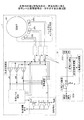
図5は、本発明の第2実施形態の一実施形態に係る信号レベル調整装置の一例を示す全体構成図である。図1に示す構成と比較すると、図5に示す構成は、信号増幅率演算を行う構成が追加される点が異なる。以下、異なる点を中心に説明する。 FIG. 5 is an overall configuration diagram showing an example of a signal level adjusting device according to an embodiment of the second embodiment of the present invention. Compared with the configuration shown in FIG. 1, the configuration shown in FIG. 5 is different in that a configuration for performing signal amplification factor calculation is added. Hereinafter, different points will be mainly described.
<検出及び調整例>
図6は、本発明の第2実施形態の一実施形態に係る信号レベル調整装置による検出及び調整の一例を示す波形図である。
<Example of detection and adjustment>
FIG. 6 is a waveform diagram showing an example of detection and adjustment by the signal level adjustment device according to one embodiment of the second embodiment of the present invention.
コモンレベルCom、平均ピークレベルPa及び平均ボトムレベルBaは、例えば、それぞれ第1実施形態と同様の方法で算出される。また、ある周期のピークレベルをP1とする。さらに、ある周期のボトムレベルをB1とする。 The common level Com, the average peak level Pa, and the average bottom level Ba are calculated by the same method as in the first embodiment, for example. In addition, the peak level of a certain period is assumed to be P1. Furthermore, the bottom level of a certain cycle is set to B1.
信号レベル調整装置は、下記(1)式によって信号増幅率Gaを計算する。
Ga=[{(P1−Pa)−(B1−Ba)}/2+Pa]/Pa (1)
さらに、信号レベル調整装置は、上記(1)式で計算される信号増幅率Gaを用いて下記(2)式によってオフセット量OFSを計算する。
OFS=−{(Ga×P1−Pa)+(Ga×B1−Ba)}/2−{(Pa+Ba)/2−Com} (2)
ゼロクロス点ZCにおいて、位相と、理想である第2グラフG2との間に、差分があると、ゼロクロス点ZCから遠ざかるに伴って、誤差が生じる場合がある。これに対して、信号レベル調整装置は、上記(1)式及び上記(2)式でそれぞれ計算される信号増幅率Ga及びオフセット量OFSに基づいてレベル調整を行う。信号増幅率Gaによってゲイン調整が行われると、第2グラフG2に近い傾きとなる第3グラフG3が生成できる。ゆえに、レベル調整が行われると、信号レベル調整装置は、ゼロクロス点ZC以外の他の点でも、位相誤差が少なくできる。したがって、信号レベル調整装置は、信号増幅率Ga及びオフセット量OFSに基づいてゲイン調整を行うと、ゼロクロス点ZC以外の他の点でも、位相誤差が少なくでき、検出する位相の精度をよくできるので、モータの回転位相検出精度を上げることができる。
The signal level adjusting device calculates the signal amplification factor Ga by the following equation (1).
Ga = [{(P1-Pa)-(B1-Ba)} / 2 + Pa] / Pa (1)
Further, the signal level adjusting device calculates the offset amount OFS by the following equation (2) using the signal amplification factor Ga calculated by the above equation (1).
OFS = − {(Ga × P1−Pa) + (Ga × B1−Ba)} / 2 − {(Pa + Ba) / 2−Com} (2)
If there is a difference between the phase and the ideal second graph G2 at the zero cross point ZC, an error may occur as the distance from the zero cross point ZC increases. On the other hand, the signal level adjusting device performs level adjustment based on the signal amplification factor Ga and the offset amount OFS calculated by the above equations (1) and (2), respectively. When gain adjustment is performed using the signal amplification factor Ga, a third graph G3 having a slope close to that of the second graph G2 can be generated. Therefore, when the level adjustment is performed, the signal level adjustment device can reduce the phase error at points other than the zero cross point ZC. Therefore, if the signal level adjustment device performs gain adjustment based on the signal amplification factor Ga and the offset amount OFS, the phase error can be reduced at other points than the zero cross point ZC, and the accuracy of the detected phase can be improved. Thus, the rotational phase detection accuracy of the motor can be increased.
[第3実施形態]
信号レベル調整装置は、位相検出信号を更に出力する構成でもよい。
[Third Embodiment]
The signal level adjusting device may be configured to further output a phase detection signal.
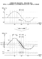
図7は、本発明の第3実施形態の一実施形態に係る信号レベル調整装置による位相検出信号の出力の一例を示す波形図である。図7は、例えば、第1実施形態又は第2実施形態に係る方法と同様の同相レベル調整によって、同相レベル調整が行われる状態を示す。即ち、図7は、第1グラフG1に示す入力信号が検出されるピークレベル及びボトムレベルに基づいてレベル調整され、第3グラフG3に示す出力信号を信号レベル調整装置が出力する例を示す。 FIG. 7 is a waveform diagram showing an example of the output of the phase detection signal by the signal level adjustment apparatus according to one embodiment of the third embodiment of the present invention. FIG. 7 shows a state in which the common-mode level adjustment is performed by the common-mode level adjustment similar to the method according to the first embodiment or the second embodiment, for example. That is, FIG. 7 shows an example in which the level is adjusted based on the peak level and the bottom level at which the input signal shown in the first graph G1 is detected, and the output signal shown in the third graph G3 is output by the signal level adjusting device.
第3実施形態では、信号レベル調整装置は、位相検出信号SIG3を出力する。具体的には、まず、第3実施形態では、「位相検出区間」、即ち、電気角が150deg乃至210degとなる区間で、スライスレベルSLVが設定される。例えば、「位相検出区間」において、第3グラフG3の信号レベルが、コモンレベルComより高い信号レベル及びコモンレベルComより低い信号レベルでそれぞれ5等分となる間隔で、スライスレベルSLVがそれぞれ設定される。 In the third embodiment, the signal level adjusting device outputs a phase detection signal SIG3. Specifically, first, in the third embodiment, the slice level SLV is set in a “phase detection section”, that is, a section in which the electrical angle is 150 deg to 210 deg. For example, in the “phase detection section”, the slice level SLV is set at intervals at which the signal level of the third graph G3 is equally divided into five at a signal level higher than the common level Com and a signal level lower than the common level Com. The
信号レベル調整装置は、それぞれのスライスレベルSLVを閾値として、位相検出信号SIG3のハイレベル及びローレベルを切り替えて出力する。具体的には、図示するように、信号レベル調整装置は、第3グラフG3の信号レベルがそれぞれのスライスレベルSLVが示すレベルになると、位相検出信号SIG3のハイレベルHLVと、ローレベルLLVとを切り替える。 The signal level adjusting device switches and outputs the high level and low level of the phase detection signal SIG3 using each slice level SLV as a threshold value. Specifically, as shown in the figure, when the signal level of the third graph G3 reaches the level indicated by each slice level SLV, the signal level adjustment device changes the high level HLV and the low level LLV of the phase detection signal SIG3. Switch.
例えば、位相検出信号SIG3がハイレベルHLVであって、第3グラフG3の信号レベルが、スライスレベルSLVが示すレベルになると、信号レベル調整装置は、位相検出信号SIG3をローレベルLLVとする。次に、第3グラフG3の信号レベルが、次のスライスレベルSLVが示すレベルになると、信号レベル調整装置は、位相検出信号SIG3をハイレベルHLVとする。 For example, when the phase detection signal SIG3 is at the high level HLV and the signal level of the third graph G3 reaches the level indicated by the slice level SLV, the signal level adjustment device sets the phase detection signal SIG3 to the low level LLV. Next, when the signal level of the third graph G3 reaches the level indicated by the next slice level SLV, the signal level adjusting device sets the phase detection signal SIG3 to the high level HLV.
第1実施形態又は第2実施形態に係る方法によって、ゼロクロス点ZCにおいて、位相が理想に近づくようにレベル調整されると、信号レベル調整装置は、ゼロクロス点ZC以外の他の点でも、位相誤差が少なくできる。したがって、信号レベル調整装置は、信号レベルが各スライスレベルSLVとなったことを示す位相検出信号SIG3を精度よく出力することができる。 When the level is adjusted so that the phase approaches the ideal at the zero-cross point ZC by the method according to the first embodiment or the second embodiment, the signal level adjustment device may also cause a phase error at other points other than the zero-cross point ZC. Can be reduced. Therefore, the signal level adjusting device can accurately output the phase detection signal SIG3 indicating that the signal level has reached each slice level SLV.
<ホール素子による出力例>
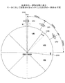
図8は、本発明の一実施形態に係るモータに対して設置されるセンサによる出力の一例を示す図である。図示するように、センサSR1乃至SR3は、例えば、それぞれモータの外側に実装される。この場合には、位相誤差は、センサを実装する精度によって決定される。なお、図8は、8極インナーロータの例を示す。即ち、図8に示す例では、モータが1回転すると、8極の磁極が切り替わる。
<Example of output by Hall element>
FIG. 8 is a diagram illustrating an example of output from a sensor installed for a motor according to an embodiment of the present invention. As shown in the figure, the sensors SR1 to SR3 are each mounted outside the motor, for example. In this case, the phase error is determined by the accuracy with which the sensor is mounted. FIG. 8 shows an example of an 8-pole inner rotor. That is, in the example shown in FIG. 8, when the motor makes one revolution, the eight magnetic poles are switched.
また、電気角の360degは、モータ角の90degに相当する。例えば、直径20mmの回転子に対して各ホール素子がそれぞれ設置されると、電気角の360degは、360deg=20×π/4=15.7mmの長さに相当する。したがって、電気角の1degは、43.6μmに相当する。即ち、センサを実装する精度が、43.6μm以下であると、位相誤差は、電気角が1deg以内に収まるが、センサを実装する精度が、43.6μmより大きいと、位相誤差が生じる場合が多い。 An electrical angle of 360 deg corresponds to a motor angle of 90 deg. For example, when each Hall element is installed on a rotor having a diameter of 20 mm, the electrical angle of 360 deg corresponds to a length of 360 deg = 20 × π / 4 = 15.7 mm. Therefore, 1 deg of the electrical angle corresponds to 43.6 μm. That is, if the accuracy of mounting the sensor is 43.6 μm or less, the phase error is within 1 deg. However, if the accuracy of mounting the sensor is greater than 43.6 μm, the phase error may occur. Many.
また、各磁極の強さにばらつきが生じると、いわゆる着磁ばらつきが生じる。着磁ばらつきが生じることによって、N極とS極との切り替わり点、即ち、センサ信号の信号レベルがコモンレベルとなるゼロクロス点で、位相誤差が生じる場合が多い。具体的には、磁極の強さが強い極は、振幅が大きくなる。一方、磁極の強さが弱い極は、振幅が小さくなる。これら磁極の強さのばらつきが、低周波成分として入力され、センサ信号に重畳する。このため、ゼロクロス点では、位相誤差が生じることが多い。また、振幅が大きい極と、振幅が小さい極とがそれぞれあると、振幅の大小によって、信号レベルの傾きは、理想的な状態と比較して異なることが多い。 Further, when variations occur in the strength of each magnetic pole, so-called magnetization variations occur. Due to the variation in magnetization, a phase error often occurs at the switching point between the N pole and the S pole, that is, at the zero cross point where the signal level of the sensor signal becomes the common level. Specifically, the pole having a strong magnetic pole has a large amplitude. On the other hand, the amplitude of a pole having a weak magnetic pole is small. Variations in the strength of these magnetic poles are input as low frequency components and are superimposed on the sensor signal. For this reason, a phase error often occurs at the zero cross point. In addition, when there are a pole having a large amplitude and a pole having a small amplitude, the slope of the signal level is often different from the ideal state depending on the magnitude of the amplitude.
回転子磁極は、1周で着磁ばらつきがある場合でも、不平衡電圧がないと、入力されるセンサ信号の振幅の平均は、着磁ばらつきがない場合の理想的なセンサ信号の振幅と一致する場合が多い。 Even if there is a variation in magnetization in one revolution of the rotor magnetic pole, if there is no unbalanced voltage, the average of the amplitude of the input sensor signal matches the ideal amplitude of the sensor signal when there is no variation in magnetization. There are many cases to do.
不平衡電圧は、ホール素子が出力する電圧にオフセット量として重畳されて出力される。なお、不平衡電圧は、無磁界の場合に、出力端子間に生じる電圧である。例えば、不平衡電圧は、ホール素子に電流又は電圧を流すと生じる残留電圧又はオフセット電圧等である。また、不平衡電圧は、ホール素子のパターンがアンバランス又は不均一であることが要因で生じる場合が多い。即ち、不平衡電圧が生じると、平均ピークレベル及び平均ボトムレベルには、コモンレベルに対して、正側又は負側に、オフセット量がある場合が多い。 The unbalanced voltage is output as an offset amount superimposed on the voltage output from the Hall element. The unbalanced voltage is a voltage generated between the output terminals when there is no magnetic field. For example, the unbalanced voltage is a residual voltage or an offset voltage generated when a current or voltage is passed through the Hall element. In many cases, the unbalanced voltage is caused by the hall element pattern being unbalanced or non-uniform. That is, when an unbalanced voltage occurs, the average peak level and the average bottom level often have an offset amount on the positive side or the negative side with respect to the common level.
本実施形態では、不平衡電圧を含む低周波成分を演算して、オフセット量を定める。1周の平均ピークレベル及び平均ボトムレベルに対して、不平衡電圧分のオフセット量が考慮されると、センサ信号は、理想的なセンサ信号に近づくことができる。 In this embodiment, the offset amount is determined by calculating a low frequency component including an unbalanced voltage. When the offset amount for the unbalanced voltage is considered with respect to the average peak level and average bottom level of one round, the sensor signal can approach an ideal sensor signal.
なお、低周波成分の演算及び信号増幅率の計算等に用いられる係数は、外部から設定されてもよい。また、説明では、位相差120degかつ3相センサ信号を利用する例で説明したが、実施形態は、これに限られず、例えば、位相差90degかつ2相センサ信号を利用する等でもよい。 Note that the coefficients used for the calculation of the low frequency component and the calculation of the signal amplification factor may be set from the outside. In the description, the example using the phase difference of 120 deg and the three-phase sensor signal has been described. However, the embodiment is not limited thereto, and for example, the phase difference of 90 deg and the two-phase sensor signal may be used.
<処理結果例>
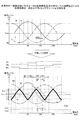
図9は、本発明の一実施形態に係るモータ駆動制御装置及び信号レベル調整装置による処理結果の一例を示すタイミングチャート及び波形図である。
<Example of processing results>
FIG. 9 is a timing chart and a waveform diagram showing an example of processing results obtained by the motor drive control device and the signal level adjustment device according to an embodiment of the present invention.
図9では、信号レベル調整装置に入力信号として入力されるセンサSR1乃至SR3(図1)が出力するセンサ信号をU、V及びWとする。即ち、図9では、センサ信号U、V及びWは、それぞれ原波形を示す。また、センサ信号U、V及びWには、位相誤差ERRが含まれる。一方、信号レベル調整装置によって同相レベル調整が行われると、出力信号U1、V1及びW1がそれぞれ生成される。 In FIG. 9, the sensor signals output from the sensors SR1 to SR3 (FIG. 1) input as input signals to the signal level adjusting device are U, V, and W. That is, in FIG. 9, the sensor signals U, V, and W each indicate an original waveform. The sensor signals U, V, and W include a phase error ERR. On the other hand, when the in-phase level adjustment is performed by the signal level adjustment device, output signals U1, V1, and W1 are generated.
さらに、図9は、交点検出信号UV、VW及びWUの例を示す。なお、図9では、U1>V1であると、交点検出信号VUは、ハイレベルとされる。また、U1<V1であると、交点検出信号VUは、ローレベルとされる。さらに、交点検出信号VW及びWUも同様とする。なお、センサ信号U、V及びWは、図1で示すように、それぞれ差動信号であるが、図9では、簡単に示すため、センサ信号U、V及びWは、それぞれの差動信号の差分を示す信号とする。 Further, FIG. 9 shows examples of the intersection detection signals UV, VW and WU. In FIG. 9, when U1> V1, the intersection detection signal VU is at a high level. If U1 <V1, the intersection detection signal VU is at a low level. The same applies to the intersection detection signals VW and WU. The sensor signals U, V, and W are differential signals as shown in FIG. 1, but in FIG. 9, for simplicity, the sensor signals U, V, and W are the differential signals. A signal indicating the difference is used.
また、選択信号X(図1)には、交点検出信号UV、VW及びWUに基づいて、例えば、(W1<U1<V1)又は(W1>U1>V1)であると、出力信号U1が選択される。また、(V1<W1<U1)又は(V1>W1>U1)であると、出力信号W1が選択される。さらに、(U1<V1<W1)又は(U1>V1>W1)であると、出力信号V1が選択される。即ち、各信号の大小は、交点検出信号UV、VW及びWUによって判定できるため、モータ駆動制御装置は、交点検出信号UV、VW及びWUに基づいて、選択信号Xを選択することができる。 The selection signal X (FIG. 1) is selected based on the intersection detection signals UV, VW, and WU, for example, if the output signal U1 is (W1 <U1 <V1) or (W1> U1> V1). Is done. If (V1 <W1 <U1) or (V1> W1> U1), the output signal W1 is selected. Further, when (U1 <V1 <W1) or (U1> V1> W1), the output signal V1 is selected. That is, since the magnitude of each signal can be determined by the intersection detection signals UV, VW, and WU, the motor drive control device can select the selection signal X based on the intersection detection signals UV, VW, and WU.
さらに、モータの回転位置に応じた複数の閾値が、例えば、スライスレベルSLVのように設定されると、選択信号XがいずれかのスライスレベルSLVとなると、モータ駆動制御装置は、選択信号Xに基づいて、位相信号としてPhsyn信号を出力し、モータ駆動制御信号とする。 Further, when a plurality of threshold values corresponding to the rotational position of the motor are set as, for example, the slice level SLV, when the selection signal X becomes any one of the slice levels SLV, the motor drive control device sets the selection signal X to Based on this, a Phsyn signal is output as a phase signal and used as a motor drive control signal.
<位相検出装置例>
図10は、本発明の一実施形態に係る位相検出装置の一例を示す構成図である。図10(A)で図示するように、位相検出装置20は、信号レベル調整装置10に対して接続される位相検出部11を有する。信号レベル調整装置10がレベル調整して出力する出力信号を位相検出部11が位相情報として出力するため、位相検出部11には、複数の閾値が設定される。
<Example of phase detector>
FIG. 10 is a configuration diagram illustrating an example of a phase detection device according to an embodiment of the present invention. As illustrated in FIG. 10A, the
また、図10(B)で図示するように、位相検出装置20は、第2実施形態の信号レベル調整装置10、即ち、ゲイン調整を行う信号レベル調整装置10と、位相検出部11とを有する構成でもよい。
Further, as illustrated in FIG. 10B, the
<モータ制御装置例>
図11は、本発明の一実施形態に係るモータ駆動制御装置の一例を示す構成図である。モータ駆動制御装置1は、モータ制御コントローラ等を有する。例えば、図1に示す信号レベル調整装置10が用いられる場合には、信号レベル調整装置10が出力する出力信号は、位相検出部によって位相情報としてモータ制御コントローラに出力される。次に、モータ制御コントローラは、位相情報に基づいて、位置及び速度等を検出し、モータを制御する。モータの制御は、例えば、PWM(Pulse Width Modulation)信号をモータ駆動部に出力することで実現される。
<Example of motor control device>
FIG. 11 is a configuration diagram illustrating an example of a motor drive control device according to an embodiment of the present invention. The motor
<搬送装置例>
図12は、本発明の一実施形態に係る搬送装置の一例を示す画像形成装置の断面図である。図12は、本発明の一実施形態に係るモータ駆動制御装置を搬送装置として画像形成装置100に適用する例である。図12に例示される画像形成装置100は、いわゆるタンデム型カラープリンタである。具体的には、画像形成装置100本体の上方にあるボトル収容部101には、各色(イエロー、マゼンタ、シアン、ブラック)に対応した4つのトナーボトル102Y、102M、102C及び102Kが着脱自在(交換自在)にそれぞれ設置される。
<Conveyor example>
FIG. 12 is a cross-sectional view of an image forming apparatus showing an example of a transport apparatus according to an embodiment of the present invention. FIG. 12 shows an example in which the motor drive control device according to one embodiment of the present invention is applied to the
また、ボトル収容部101の下方には、中間転写ユニット85が配設される。その中間転写ユニット85が有する中間転写ベルト78に対向するように、各色に対応する作像部74Y、74M、74C及び74Kがそれぞれ並設される。
In addition, an
さらに、各作像部74Y、74M、74C及び74Kには、それぞれ感光体ドラム75Y、75M、75C及び75Kが配設される。また、各感光体ドラム75Y、75M、75C、及び75Kの周囲には、それぞれ帯電部73、現像部76、クリーニング部77及び除電部等がそれぞれ配設される。そして、各感光体ドラム75Y、75M、75C及び75Kで、作像プロセス(帯電工程、露光工程、現像工程、転写工程及びクリーニング工程)がそれぞれ行われ、各感光体ドラム75Y、75M、75C及び75K上に、各色の画像が形成される。
Further,
感光体ドラム75Y、75M、75C及び75Kは、駆動モータによって時計方向にそれぞれ回転駆動される。そして、帯電部73の位置で、感光体ドラム75Y、75M、75C及び75Kの表面が一様にそれぞれ帯電される(帯電工程の例)。
The
帯電工程の後、感光体ドラム75Y、75M、75C及び75Kの表面には、露光部103から発せられるレーザ光の照射位置に、露光走査によって各色に対応する静電潜像がそれぞれ形成される(露光工程の例)。
After the charging step, electrostatic latent images corresponding to the respective colors are formed on the surfaces of the
露光工程の後、感光体ドラム75Y、75M、75C及び75Kの表面には、現像部76との対向位置に、静電潜像が現像され、各色のトナー像がそれぞれ形成される(現像工程の例)。
After the exposure process, the electrostatic latent images are developed on the surfaces of the
現像工程の後、感光体ドラム75Y、75M、75C及び75Kの表面には、中間転写ベルト78及び第1転写バイアスローラ79Y、79M、79C及び79Kとの対向位置に、感光体ドラム75Y、75M、75C及び75K上のそれぞれのトナー像が中間転写ベルト78上にそれぞれ転写される(1次転写工程の例)。1次転写が行われると、それぞれの感光体ドラム75Y、75M、75C及び75K上には、未転写トナーが残存する場合がある。
After the development process, the
1次転写工程の後、感光体ドラム75Y、75M、75C及び75Kの表面では、クリーニング部77との対向位置で、感光体ドラム75Y、75M、75C及び75K上に残存した未転写トナーがクリーニング部77のクリーニングブレードによって機械的にそれぞれ回収される(クリーニング工程の例)。
After the primary transfer process, untransferred toner remaining on the
次に、感光体ドラム75Y、75M、75C及び75Kの表面では、除電部との対向位置で、感光体ドラム75Y、75M、75C及び75K上の残留電位が除去される。こうして、感光体ドラム75Y、75M、75C及び75K上でそれぞれ行われる一連の作像プロセスが終了する。
Next, on the surfaces of the
ここで、搬送される記録媒体Pは、2次転写ニップの位置に、画像形成装置100の下方に配設される給紙部104から、給紙ローラ97又はレジストローラ対98等によって搬送される。
Here, the recording medium P to be transported is transported to the position of the secondary transfer nip from a
詳しくは、給紙部104には、転写紙等の記録媒体Pが複数枚重ねて収納される。そして、給紙ローラ97が反時計方向に回転駆動すると、一番上の記録媒体Pが、レジストローラ対98のローラ間に向けて給送される。
Specifically, a plurality of recording media P such as transfer paper are stored in the
レジストローラ対98に搬送された記録媒体Pは、回転駆動を停止したレジストローラ対98のローラニップの位置で一旦停止する。そして、中間転写ベルト78上のカラー画像にタイミングを合わせて、レジストローラ対98が回転駆動されて、記録媒体Pが2次転写ニップに向けて搬送される。こうして、記録媒体P上に、所望のカラー画像が転写される。
The recording medium P conveyed to the registration roller pair 98 is temporarily stopped at the position of the roller nip of the registration roller pair 98 that has stopped rotating. Then, the registration roller pair 98 is rotationally driven in synchronization with the color image on the
その後、2次転写ニップの位置でカラー画像が転写された記録媒体Pは、定着装置90の位置に搬送される。そして、この位置で、定着ローラ91及び加圧ローラ92による熱と圧力とにより、表面に転写されたカラー画像が、記録媒体P上に定着される。
Thereafter, the recording medium P on which the color image is transferred at the position of the secondary transfer nip is conveyed to the position of the fixing
続いて、記録媒体Pは、排紙ローラ対99のローラ間を経て、装置外へと排出される。排紙ローラ対99によって装置外に排出された記録媒体Pは、スタック部93上に順次スタックされる。こうして、画像形成装置100における、一連の画像形成プロセスが完了する。
Subsequently, the recording medium P is discharged out of the apparatus through a pair of
実施形態に係るモータ駆動制御装置により制御されるモータは、上述したレジストローラ対98等を駆動させる動力として用いることができる。例えば、記録媒体Pをレジストローラ対98のローラニップの位置で一旦停止させる際のモータのモータ駆動モードを、位置ホールドモードとする。位置ホールドモードによりモータの回転駆動を停止させることで、モータ、即ち、レジストローラ対98の回転位置が保持され、記録媒体Pの位置が保持される。 The motor controlled by the motor drive control device according to the embodiment can be used as power for driving the above-described registration roller pair 98 and the like. For example, the motor drive mode of the motor when the recording medium P is temporarily stopped at the position of the roller nip of the registration roller pair 98 is a position hold mode. By stopping the rotational drive of the motor in the position hold mode, the rotational position of the motor, that is, the registration roller pair 98 is held, and the position of the recording medium P is held.
実施形態によれば、位置ホールド状態で記録媒体Pの位置を保持する期間は、モータが駆動周期ごとに反転制御される。そのため、ロック状態を検知するカウント値が駆動周期ごとにリセットされるため、閾値を超えることが無く、長時間、記録媒体Pの停止状態が継続しても、ロック状態と誤検知されることが少ない。 According to the embodiment, during the period in which the position of the recording medium P is held in the position hold state, the motor is reversely controlled for each drive cycle. For this reason, the count value for detecting the locked state is reset for each driving cycle, so that the threshold value is not exceeded and even if the stopped state of the recording medium P continues for a long time, it is erroneously detected as the locked state. Few.
なお、実施形態に係るモータ駆動制御装置によって制御されるモータは、レジストローラ対98の駆動源に限られず、画像形成装置100において位置を保持する駆動制御が必要な他の動力源として適用してもよい。
Note that the motor controlled by the motor drive control device according to the embodiment is not limited to the drive source of the registration roller pair 98, and is applied as another power source that requires drive control to hold the position in the
以上、本発明の好ましい実施例について詳述したが、本発明は係る特定の実施形態に限定されるものではなく、特許請求の範囲に記載された本発明の要旨の範囲内において、種々の変形又は変更が可能である。 The preferred embodiments of the present invention have been described in detail above, but the present invention is not limited to such specific embodiments, and various modifications can be made within the scope of the gist of the present invention described in the claims. Or it can be changed.
1 モータ駆動制御装置
10 信号レベル調整装置
20 位相検出装置
100 画像形成装置
DESCRIPTION OF
Claims (10)
前記検出手段が検出した前記入力信号の複数回のピークレベル及びボトムレベルに基づいて、前記入力信号の所定区間でレベル調整を行うレベル調整手段と
を備えた信号レベル調整装置。 Detecting means for detecting a peak level and a bottom level of an input signal in accordance with a sine wave or a sine wave;
A signal level adjustment device comprising level adjustment means for performing level adjustment in a predetermined section of the input signal based on a plurality of peak levels and bottom levels of the input signal detected by the detection means.
前記信号レベル調整装置が、正弦波若しくは正弦波に準じた入力信号のピークレベル及びボトムレベルをそれぞれ検出する検出手順と、
前記信号レベル調整装置が、前記検出手順で検出した前記入力信号の複数回のピークレベル及びボトムレベルに基づいて、前記入力信号の所定区間でレベル調整を行うレベル調整手順と
を含む信号レベル調整方法。 A signal level adjustment method performed by the signal level adjustment device,
A detection procedure in which the signal level adjusting device detects a peak level and a bottom level of an input signal in accordance with a sine wave or a sine wave, respectively;
A signal level adjustment method, wherein the signal level adjustment device includes a level adjustment procedure for performing level adjustment in a predetermined section of the input signal based on a plurality of peak levels and bottom levels of the input signal detected by the detection procedure. .
Priority Applications (2)
| Application Number | Priority Date | Filing Date | Title |
|---|---|---|---|
| JP2015123234A JP2017009355A (en) | 2015-06-18 | 2015-06-18 | Signal level adjustment device, phase detection device, motor drive control device, transport device, and signal level adjustment method |
| US15/179,348 US10401768B2 (en) | 2015-06-18 | 2016-06-10 | Signal level, adjustment apparatus, phase detection apparatus, motor drive controller, conveyer, image forming apparatus, and signal level adjustment method |
Applications Claiming Priority (1)
| Application Number | Priority Date | Filing Date | Title |
|---|---|---|---|
| JP2015123234A JP2017009355A (en) | 2015-06-18 | 2015-06-18 | Signal level adjustment device, phase detection device, motor drive control device, transport device, and signal level adjustment method |
Publications (1)
| Publication Number | Publication Date |
|---|---|
| JP2017009355A true JP2017009355A (en) | 2017-01-12 |
Family
ID=57587883
Family Applications (1)
| Application Number | Title | Priority Date | Filing Date |
|---|---|---|---|
| JP2015123234A Pending JP2017009355A (en) | 2015-06-18 | 2015-06-18 | Signal level adjustment device, phase detection device, motor drive control device, transport device, and signal level adjustment method |
Country Status (2)
| Country | Link |
|---|---|
| US (1) | US10401768B2 (en) |
| JP (1) | JP2017009355A (en) |
Families Citing this family (1)
| Publication number | Priority date | Publication date | Assignee | Title |
|---|---|---|---|---|
| JP2018021884A (en) | 2016-08-05 | 2018-02-08 | 株式会社リコー | Phase detection device, motor system, image forming apparatus, conveying device, and sensor level acquiring method |
Family Cites Families (7)
| Publication number | Priority date | Publication date | Assignee | Title |
|---|---|---|---|---|
| DE3889283T2 (en) * | 1987-10-16 | 1994-09-01 | Canon Kk | Imaging device. |
| JP4708992B2 (en) * | 2005-12-12 | 2011-06-22 | 日立オートモティブシステムズ株式会社 | Position detecting apparatus and synchronous motor driving apparatus using the same |
| JP2013108971A (en) * | 2011-10-25 | 2013-06-06 | Ricoh Co Ltd | Angle detector, motor drive device, and image forming apparatus |
| JP5919730B2 (en) | 2011-10-28 | 2016-05-18 | 株式会社リコー | Motor drive control apparatus and method |
| JP6014989B2 (en) | 2011-10-28 | 2016-10-26 | 株式会社リコー | Motor drive control apparatus and method |
| JP2015019563A (en) | 2013-06-10 | 2015-01-29 | 株式会社リコー | Control device, drive device, and image forming apparatus |
| JP6387667B2 (en) | 2014-04-21 | 2018-09-12 | 株式会社リコー | Signal amplification device and motor drive control device including the same |
-
2015
- 2015-06-18 JP JP2015123234A patent/JP2017009355A/en active Pending
-
2016
- 2016-06-10 US US15/179,348 patent/US10401768B2/en active Active
Also Published As
| Publication number | Publication date |
|---|---|
| US20160370746A1 (en) | 2016-12-22 |
| US10401768B2 (en) | 2019-09-03 |
Similar Documents
| Publication | Publication Date | Title |
|---|---|---|
| JP5942696B2 (en) | Motor control device, motor control method, and image forming apparatus | |
| JP6745659B2 (en) | Motor control device, sheet conveying device, and image forming device | |
| US10547263B2 (en) | Motor driving apparatus, sheet conveyance apparatus, document feeding apparatus, document reading apparatus and image forming apparatus | |
| JP2015019563A (en) | Control device, drive device, and image forming apparatus | |
| US9787241B2 (en) | Motor driving device for controlling motor with pulse signal | |
| US20240061365A1 (en) | Motor control apparatus and image forming apparatus with limiting coil current flowing through motor coil | |
| JP2015105844A (en) | Rotation angle detection device, image processing device, and rotation angle detection method | |
| US9961221B2 (en) | Motor control apparatus that controls motor based on result of detection by position detection sensor that detects rotational position of rotor of motor, and image forming apparatus | |
| JP2015192538A (en) | Stepping motor drive device, image carrier rotation drive device, and image forming apparatus | |
| US9419557B2 (en) | Motor control device, image forming apparatus, and motor control method | |
| US11329580B2 (en) | Motor control apparatus and image forming apparatus | |
| US10401768B2 (en) | Signal level, adjustment apparatus, phase detection apparatus, motor drive controller, conveyer, image forming apparatus, and signal level adjustment method | |
| JP6790938B2 (en) | Motor control device, angle estimation device and image forming device | |
| JP5641819B2 (en) | Image forming apparatus | |
| JP5899808B2 (en) | Image forming apparatus | |
| JP5621960B2 (en) | Motor drive device and image forming apparatus | |
| JP6770610B2 (en) | Motor drive device and image forming device | |
| JP6142742B2 (en) | Optical scanning apparatus, image forming apparatus, and sensor signal discrimination method | |
| JP6569635B2 (en) | Motor control device and image forming apparatus | |
| JP6432129B2 (en) | Angle detection device and angle detection method | |
| US12601997B2 (en) | Image forming apparatus that detects stopping position of rotor of motor | |
| JP2015167458A (en) | Motor control device and image forming device | |
| JP6798306B2 (en) | Phase adjuster, phase detector, motor drive, motor drive system, image forming device, and transfer device | |
| JP2022129004A (en) | Image forming apparatus | |
| JP6508516B2 (en) | Image forming device |