JP2017102811A - Display device and input device - Google Patents
Display device and input device Download PDFInfo
- Publication number
- JP2017102811A JP2017102811A JP2015237258A JP2015237258A JP2017102811A JP 2017102811 A JP2017102811 A JP 2017102811A JP 2015237258 A JP2015237258 A JP 2015237258A JP 2015237258 A JP2015237258 A JP 2015237258A JP 2017102811 A JP2017102811 A JP 2017102811A
- Authority
- JP
- Japan
- Prior art keywords
- detection
- electrode
- electrodes
- display device
- capacitance
- Prior art date
- Legal status (The legal status is an assumption and is not a legal conclusion. Google has not performed a legal analysis and makes no representation as to the accuracy of the status listed.)
- Granted
Links
Images











Classifications
-
- G—PHYSICS
- G06—COMPUTING OR CALCULATING; COUNTING
- G06F—ELECTRIC DIGITAL DATA PROCESSING
- G06F3/00—Input arrangements for transferring data to be processed into a form capable of being handled by the computer; Output arrangements for transferring data from processing unit to output unit, e.g. interface arrangements
- G06F3/01—Input arrangements or combined input and output arrangements for interaction between user and computer
- G06F3/03—Arrangements for converting the position or the displacement of a member into a coded form
- G06F3/041—Digitisers, e.g. for touch screens or touch pads, characterised by the transducing means
- G06F3/0412—Digitisers structurally integrated in a display
-
- G—PHYSICS
- G02—OPTICS
- G02F—OPTICAL DEVICES OR ARRANGEMENTS FOR THE CONTROL OF LIGHT BY MODIFICATION OF THE OPTICAL PROPERTIES OF THE MEDIA OF THE ELEMENTS INVOLVED THEREIN; NON-LINEAR OPTICS; FREQUENCY-CHANGING OF LIGHT; OPTICAL LOGIC ELEMENTS; OPTICAL ANALOGUE/DIGITAL CONVERTERS
- G02F1/00—Devices or arrangements for the control of the intensity, colour, phase, polarisation or direction of light arriving from an independent light source, e.g. switching, gating or modulating; Non-linear optics
- G02F1/01—Devices or arrangements for the control of the intensity, colour, phase, polarisation or direction of light arriving from an independent light source, e.g. switching, gating or modulating; Non-linear optics for the control of the intensity, phase, polarisation or colour
- G02F1/13—Devices or arrangements for the control of the intensity, colour, phase, polarisation or direction of light arriving from an independent light source, e.g. switching, gating or modulating; Non-linear optics for the control of the intensity, phase, polarisation or colour based on liquid crystals, e.g. single liquid crystal display cells
- G02F1/133—Constructional arrangements; Operation of liquid crystal cells; Circuit arrangements
- G02F1/1333—Constructional arrangements; Manufacturing methods
- G02F1/13338—Input devices, e.g. touch panels
-
- G—PHYSICS
- G02—OPTICS
- G02F—OPTICAL DEVICES OR ARRANGEMENTS FOR THE CONTROL OF LIGHT BY MODIFICATION OF THE OPTICAL PROPERTIES OF THE MEDIA OF THE ELEMENTS INVOLVED THEREIN; NON-LINEAR OPTICS; FREQUENCY-CHANGING OF LIGHT; OPTICAL LOGIC ELEMENTS; OPTICAL ANALOGUE/DIGITAL CONVERTERS
- G02F1/00—Devices or arrangements for the control of the intensity, colour, phase, polarisation or direction of light arriving from an independent light source, e.g. switching, gating or modulating; Non-linear optics
- G02F1/01—Devices or arrangements for the control of the intensity, colour, phase, polarisation or direction of light arriving from an independent light source, e.g. switching, gating or modulating; Non-linear optics for the control of the intensity, phase, polarisation or colour
- G02F1/13—Devices or arrangements for the control of the intensity, colour, phase, polarisation or direction of light arriving from an independent light source, e.g. switching, gating or modulating; Non-linear optics for the control of the intensity, phase, polarisation or colour based on liquid crystals, e.g. single liquid crystal display cells
- G02F1/133—Constructional arrangements; Operation of liquid crystal cells; Circuit arrangements
- G02F1/1333—Constructional arrangements; Manufacturing methods
- G02F1/1343—Electrodes
- G02F1/134309—Electrodes characterised by their geometrical arrangement
- G02F1/134336—Matrix
-
- G—PHYSICS
- G06—COMPUTING OR CALCULATING; COUNTING
- G06F—ELECTRIC DIGITAL DATA PROCESSING
- G06F3/00—Input arrangements for transferring data to be processed into a form capable of being handled by the computer; Output arrangements for transferring data from processing unit to output unit, e.g. interface arrangements
- G06F3/01—Input arrangements or combined input and output arrangements for interaction between user and computer
- G06F3/03—Arrangements for converting the position or the displacement of a member into a coded form
- G06F3/041—Digitisers, e.g. for touch screens or touch pads, characterised by the transducing means
- G06F3/0416—Control or interface arrangements specially adapted for digitisers
- G06F3/04166—Details of scanning methods, e.g. sampling time, grouping of sub areas or time sharing with display driving
-
- G—PHYSICS
- G06—COMPUTING OR CALCULATING; COUNTING
- G06F—ELECTRIC DIGITAL DATA PROCESSING
- G06F3/00—Input arrangements for transferring data to be processed into a form capable of being handled by the computer; Output arrangements for transferring data from processing unit to output unit, e.g. interface arrangements
- G06F3/01—Input arrangements or combined input and output arrangements for interaction between user and computer
- G06F3/03—Arrangements for converting the position or the displacement of a member into a coded form
- G06F3/041—Digitisers, e.g. for touch screens or touch pads, characterised by the transducing means
- G06F3/044—Digitisers, e.g. for touch screens or touch pads, characterised by the transducing means by capacitive means
- G06F3/0443—Digitisers, e.g. for touch screens or touch pads, characterised by the transducing means by capacitive means using a single layer of sensing electrodes
-
- G—PHYSICS
- G02—OPTICS
- G02F—OPTICAL DEVICES OR ARRANGEMENTS FOR THE CONTROL OF LIGHT BY MODIFICATION OF THE OPTICAL PROPERTIES OF THE MEDIA OF THE ELEMENTS INVOLVED THEREIN; NON-LINEAR OPTICS; FREQUENCY-CHANGING OF LIGHT; OPTICAL LOGIC ELEMENTS; OPTICAL ANALOGUE/DIGITAL CONVERTERS
- G02F1/00—Devices or arrangements for the control of the intensity, colour, phase, polarisation or direction of light arriving from an independent light source, e.g. switching, gating or modulating; Non-linear optics
- G02F1/01—Devices or arrangements for the control of the intensity, colour, phase, polarisation or direction of light arriving from an independent light source, e.g. switching, gating or modulating; Non-linear optics for the control of the intensity, phase, polarisation or colour
- G02F1/13—Devices or arrangements for the control of the intensity, colour, phase, polarisation or direction of light arriving from an independent light source, e.g. switching, gating or modulating; Non-linear optics for the control of the intensity, phase, polarisation or colour based on liquid crystals, e.g. single liquid crystal display cells
- G02F1/133—Constructional arrangements; Operation of liquid crystal cells; Circuit arrangements
- G02F1/1333—Constructional arrangements; Manufacturing methods
- G02F1/1343—Electrodes
- G02F1/13439—Electrodes characterised by their electrical, optical, physical properties; materials therefor; method of making
-
- G—PHYSICS
- G06—COMPUTING OR CALCULATING; COUNTING
- G06F—ELECTRIC DIGITAL DATA PROCESSING
- G06F2203/00—Indexing scheme relating to G06F3/00 - G06F3/048
- G06F2203/041—Indexing scheme relating to G06F3/041 - G06F3/045
- G06F2203/04107—Shielding in digitiser, i.e. guard or shielding arrangements, mostly for capacitive touchscreens, e.g. driven shields, driven grounds
-
- G—PHYSICS
- G06—COMPUTING OR CALCULATING; COUNTING
- G06F—ELECTRIC DIGITAL DATA PROCESSING
- G06F2203/00—Indexing scheme relating to G06F3/00 - G06F3/048
- G06F2203/041—Indexing scheme relating to G06F3/041 - G06F3/045
- G06F2203/04108—Touchless 2D- digitiser, i.e. digitiser detecting the X/Y position of the input means, finger or stylus, also when it does not touch, but is proximate to the digitiser's interaction surface without distance measurement in the Z direction
Landscapes
- Engineering & Computer Science (AREA)
- Physics & Mathematics (AREA)
- Theoretical Computer Science (AREA)
- General Engineering & Computer Science (AREA)
- General Physics & Mathematics (AREA)
- Nonlinear Science (AREA)
- Human Computer Interaction (AREA)
- Crystallography & Structural Chemistry (AREA)
- Optics & Photonics (AREA)
- Chemical & Material Sciences (AREA)
- Mathematical Physics (AREA)
- Geometry (AREA)
- Position Input By Displaying (AREA)
- Liquid Crystal (AREA)
- Devices For Indicating Variable Information By Combining Individual Elements (AREA)
Abstract
【課題】待機モードとして行われる検出処理に要する時間を短くし、消費電力を低減しつつ、検出ミスの発生を防止または抑制することができる入力装置および表示装置を提供することを目的とする。【解決手段】前面FSおよび背面BSを有し、前面FSに画像が表示される表示パネルPNLと、平面視において表示パネルPNLと重なる複数の検出電極Rxと、平面視において表示パネルPNLと重なるシールド電極SHと、を有する。シールド電極SHは、複数の検出電極Rxに対して前面FS側と反対側に配置されている。シールド電極SHの静電容量に基づいて、前面FSへの物体の近接または接触が検出され、複数の検出電極Rxの各々の静電容量に基づいて、物体の位置が検出される。【選択図】図3An object of the present invention is to provide an input device and a display device that can prevent or suppress the occurrence of detection errors while shortening the time required for detection processing performed in a standby mode and reducing power consumption. A display panel PNL having a front surface FS and a back surface BS and displaying an image on the front surface FS, a plurality of detection electrodes Rx overlapping the display panel PNL in plan view, and a shield overlapping the display panel PNL in plan view And an electrode SH. The shield electrode SH is disposed on the side opposite to the front surface FS side with respect to the plurality of detection electrodes Rx. The proximity or contact of the object to the front surface FS is detected based on the capacitance of the shield electrode SH, and the position of the object is detected based on the capacitance of each of the plurality of detection electrodes Rx. [Selection] Figure 3
Description
本発明は表示装置および入力装置に関する。 The present invention relates to a display device and an input device.
近年、表示装置の表示面側に、タッチパネルあるいはタッチセンサと呼ばれる入力装置を取り付け、タッチパネルに指やタッチペンなどの入力具などを接触させて入力動作を行ったときに、入力位置を検出して出力する技術がある。 In recent years, when an input device called a touch panel or touch sensor is attached to the display surface side of a display device and an input tool such as a finger or a touch pen is brought into contact with the touch panel to perform an input operation, the input position is detected and output. There is technology to do.
このような入力装置としてのタッチパネルに指などが接触した接触位置を検出する検出方式の一つとして、静電容量方式がある。静電容量方式を用いたタッチパネルでは、タッチパネルの面内に、検出電極からなる容量素子が複数個設けられている。そして、指やタッチペンなどの入力具を容量素子に接触させて入力動作を行ったときに、容量素子の静電容量が変化することを利用して、入力位置を検出する。 As one of detection methods for detecting a contact position where a finger or the like touches a touch panel as such an input device, there is a capacitance method. In a touch panel using a capacitance method, a plurality of capacitive elements including detection electrodes are provided in the surface of the touch panel. Then, when an input operation is performed by bringing an input tool such as a finger or a touch pen into contact with the capacitive element, the input position is detected by utilizing the change in capacitance of the capacitive element.
例えば、特開2015−121958号公報(特許文献1)には、入力装置において、検出電極と、検出電極と交差するように配置され、検出電極との間でそれぞれ静電容量を形成する複数の駆動電極と、検出電極および複数の駆動電極と比べて操作面から離れた下層に配置されたシールド電極と、を有する技術が記載されている。 For example, in Japanese Unexamined Patent Application Publication No. 2015-121958 (Patent Document 1), in an input device, a plurality of detection electrodes and a plurality of electrodes that are arranged so as to intersect with the detection electrodes and respectively form capacitance between the detection electrodes. A technique is described that includes a drive electrode and a shield electrode disposed in a lower layer farther from the operation surface than the detection electrode and the plurality of drive electrodes.
このような入力装置において、検出モードとして、指の位置、すなわち指の座標を検出する指座標検出処理を行う前に、待機モードとして、指の近接または接触を検出する指近接検出処理を行うことがある。また、指座標検出処理では、複数の検出電極を1個ずつまたは複数個ずつ順次切り替えて検出回路に接続することにより、複数の検出電極の各々の静電容量を個別に検出する。 In such an input device, as the detection mode, the finger proximity detection process for detecting the proximity or contact of the finger is performed as the standby mode before the finger coordinate detection process for detecting the finger position, that is, the finger coordinates is performed. There is. In the finger coordinate detection process, the capacitance of each of the plurality of detection electrodes is individually detected by switching the plurality of detection electrodes one by one or sequentially and connecting them to the detection circuit.
しかし、指近接検出処理において、指座標検出処理と同様に、複数の検出電極を複数個ずつ切り替えて検出回路に接続することにより、複数の検出電極の各々の静電容量を検出する場合、検出処理に要する時間が長くなるか、または、消費電力が増加するという問題がある。 However, in the finger proximity detection process, as in the finger coordinate detection process, when detecting the capacitance of each of the plurality of detection electrodes by switching a plurality of detection electrodes and connecting them to the detection circuit, detection is performed. There is a problem that the time required for processing becomes long or power consumption increases.
一方、検出処理に要する時間を短くするために、複数の検出電極のうち一部から複数個ずつ選択するか、または、検出処理を繰り返す間の待ち時間を長くした場合、検出ミスが発生するおそれがある。 On the other hand, in order to shorten the time required for the detection process, if a plurality of detection electrodes are selected from some of the detection electrodes or the waiting time during the detection process is increased, a detection error may occur. There is.
本発明は、上述のような従来技術の問題点を解決すべくなされたものであって、検出モードとしての指座標検出処理の前に待機モードとして行われる指近接検出処理において、検出処理に要する時間を短くし、消費電力を低減しつつ、検出ミスの発生を防止または抑制することができる入力装置および表示装置を提供することを目的とする。 The present invention has been made to solve the above-described problems of the prior art, and is required for detection processing in finger proximity detection processing performed as a standby mode before finger coordinate detection processing as detection mode. An object of the present invention is to provide an input device and a display device that can prevent or suppress the occurrence of a detection error while shortening the time and reducing the power consumption.
本願において開示される発明のうち、代表的なものの概要を簡単に説明すれば、次のとおりである。 Of the inventions disclosed in the present application, the outline of typical ones will be briefly described as follows.
本発明の一態様としての表示装置は、第1の側の第1面、および、第1の側と反対側の第2面を有し、第1面に画像が表示される表示パネルと、平面視において表示パネルと重なる複数の第1電極と、平面視において表示パネルと重なる第2電極と、を有する。第2電極は、複数の第1電極に対して第1の側と反対側に配置されている。第2電極の静電容量に基づいて、第1面への物体の近接または接触が検出され、複数の第1電極の各々の静電容量に基づいて、第1面に近接または接触した物体の位置が検出される。 A display device as one embodiment of the present invention includes a display panel having a first surface on a first side and a second surface opposite to the first side, and an image is displayed on the first surface; A plurality of first electrodes that overlap the display panel in plan view and a second electrode that overlaps the display panel in plan view. The second electrode is disposed on the opposite side to the first side with respect to the plurality of first electrodes. Based on the capacitance of the second electrode, the proximity or contact of the object to the first surface is detected, and based on the capacitance of each of the plurality of first electrodes, the proximity of or contact to the first surface of the object The position is detected.
また、本発明の一態様としての入力装置は、第1の側の第1面、および、第1の側と反対側の第2面を有する基板と、平面視において基板と重なる複数の第1電極と、平面視において基板と重なる第2電極と、を有する。第2電極は、複数の第1電極に対して第1の側と反対側に配置されている。第2電極の静電容量に基づいて、第1面への物体の近接または接触が検出され、複数の第1電極の各々の静電容量に基づいて、第1面に近接または接触した物体の位置が検出される。 An input device as one embodiment of the present invention includes a substrate having a first surface on the first side and a second surface opposite to the first side, and a plurality of first surfaces overlapping the substrate in plan view. An electrode and a second electrode overlapping the substrate in plan view. The second electrode is disposed on the opposite side to the first side with respect to the plurality of first electrodes. Based on the capacitance of the second electrode, the proximity or contact of the object to the first surface is detected, and based on the capacitance of each of the plurality of first electrodes, the proximity of or contact to the first surface of the object The position is detected.
以下に、本発明の各実施の形態について、図面を参照しつつ説明する。 Hereinafter, embodiments of the present invention will be described with reference to the drawings.
なお、開示はあくまで一例にすぎず、当業者において、発明の主旨を保っての適宜変更について容易に想到し得るものについては、当然に本発明の範囲に含有されるものである。また、図面は説明をより明確にするため、実施の態様に比べ、各部の幅、厚さ、形状等について模式的に表される場合があるが、あくまで一例であって、本発明の解釈を限定するものではない。 It should be noted that the disclosure is merely an example, and those skilled in the art can easily conceive of appropriate modifications while maintaining the gist of the invention are naturally included in the scope of the present invention. In addition, the drawings may be schematically represented with respect to the width, thickness, shape, and the like of each part as compared with the embodiments for the sake of clarity of explanation, but are merely examples, and the interpretation of the present invention is not limited thereto. It is not limited.
また本明細書と各図において、既出の図に関して前述したものと同様の要素には、同一の符号を付して、詳細な説明を適宜省略することがある。 In addition, in the present specification and each drawing, elements similar to those described above with reference to the previous drawings are denoted by the same reference numerals, and detailed description may be omitted as appropriate.
さらに、実施の形態で用いる図面においては、構造物を区別するために付したハッチング(網掛け)を図面に応じて省略する場合もある。 Furthermore, in the drawings used in the embodiments, hatching (shading) attached to distinguish structures may be omitted depending on the drawings.
(実施の形態1)
初めに、実施の形態1として、入力装置としてのタッチパネルを、入力装置の検出電極が、表示装置の表示パネル内に設けられ、かつ、表示装置の共通電極として機能するインセル型のタッチ検出機能付き表示装置に適用した例について説明する。ここで、本実施の形態1の表示装置は、液晶表示装置である。なお、本願明細書では、入力装置とは、少なくとも電極に対して近接または接触する物体の容量に応じて変化する静電容量を検出する入力装置である。ここで、静電容量を検出する方式としては、1つの電極の静電容量を検出する自己容量方式を用いることができる。また、インセル型のタッチ検出機能付き表示装置とは、タッチ検出用の駆動電極または検出電極が、画素による画像表示用の駆動電極として機能する、という特徴を持つタッチ検出機能付き表示装置を意味する。
(Embodiment 1)
First, as a first embodiment, a touch panel as an input device is provided, a detection electrode of the input device is provided in a display panel of the display device, and an in-cell type touch detection function functions as a common electrode of the display device. An example applied to a display device will be described. Here, the display device of the first embodiment is a liquid crystal display device. In the specification of the present application, the input device is an input device that detects a capacitance that changes according to the capacitance of an object that is at least in contact with or in contact with an electrode. Here, as a method for detecting the capacitance, a self-capacitance method for detecting the capacitance of one electrode can be used. The in-cell type display device with a touch detection function means a display device with a touch detection function having a feature that a drive electrode or a detection electrode for touch detection functions as a drive electrode for image display using pixels. .
<表示装置>
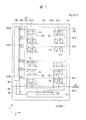
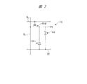
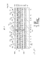
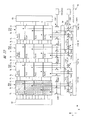
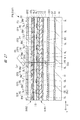
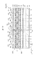
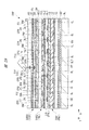
図1は、実施の形態1の表示装置の一例を示す平面図である。図2は、実施の形態1の表示装置における画素を示す等価回路図である。図3は、実施の形態1の表示装置の一例を示す断面図である。図4は、実施の形態1の表示装置における共通電極の配置の一例を示す平面図である。なお、図3では、実際には図3の断面には配置されていない走査線GLを便宜上一緒に示している。
<Display device>
FIG. 1 is a plan view illustrating an example of the display device according to the first embodiment. FIG. 2 is an equivalent circuit diagram illustrating a pixel in the display device of the first embodiment. FIG. 3 is a cross-sectional view illustrating an example of the display device of the first embodiment. FIG. 4 is a plan view showing an example of the arrangement of common electrodes in the display device of the first embodiment. In FIG. 3, the scanning lines GL that are not actually arranged in the cross section of FIG. 3 are shown together for convenience.
図1に示すように、液晶表示装置としての表示装置DSPは、アクティブマトリクス型の液晶表示パネルとしての表示パネルPNL、表示パネルPNLを駆動する駆動ICチップIC1、および、静電容量型の検出部SEを有する。表示パネルPNLは、第1の側(図3中上側)の前面FS、および、第1の側と反対側(図3中下側)の背面BSを有し、前面FSに画像が表示される。また、タッチ検出回路としての検出部SEおよび検出部SEによる検出方法については、後述する図14〜図19を用いて説明する。なお、図示は省略するが、表示装置DSPは、表示パネルPNLの外部に設けられた制御モジュール、表示パネルPNLと制御モジュールとを接続するフレキシブル配線基板、および、検出部SEを駆動する駆動ICチップなどを有してもよい。 As shown in FIG. 1, a display device DSP as a liquid crystal display device includes a display panel PNL as an active matrix type liquid crystal display panel, a driving IC chip IC1 for driving the display panel PNL, and a capacitance type detection unit. Has SE. The display panel PNL has a front surface FS on the first side (upper side in FIG. 3) and a rear surface BS on the opposite side to the first side (lower side in FIG. 3), and an image is displayed on the front surface FS. . A detection unit SE as a touch detection circuit and a detection method by the detection unit SE will be described with reference to FIGS. Although not shown, the display device DSP includes a control module provided outside the display panel PNL, a flexible wiring board that connects the display panel PNL and the control module, and a driving IC chip that drives the detection unit SE. And so on.
図1および図3に示すように、液晶表示パネルとしての表示パネルPNLは、基板SUB1と、基板SUB1と対向配置された基板SUB2と、基板SUB1と基板SUB2との間に配置された液晶層LQと、を含む。基板SUB2は、基板SUB1に対して第1の側(図3中上側)に配置されている。なお、本実施の形態1において、基板SUB1をアレイ基板と言い換えることができ、基板SUB2を対向基板と言い換えることができる。 As shown in FIGS. 1 and 3, the display panel PNL as a liquid crystal display panel includes a substrate SUB1, a substrate SUB2 disposed opposite to the substrate SUB1, and a liquid crystal layer LQ disposed between the substrate SUB1 and the substrate SUB2. And including. The substrate SUB2 is disposed on the first side (upper side in FIG. 3) with respect to the substrate SUB1. In the first embodiment, the substrate SUB1 can be rephrased as an array substrate, and the substrate SUB2 can be rephrased as a counter substrate.
また、図3および図4に示すように、表示装置DSPは、表示パネルPNLの内部に配置された複数の検出電極Rxを有する。複数の検出電極Rxは、平面視において表示パネルPNLと重なる。また、複数の検出電極Rxは、基板SUB1と液晶層LQとの間に配置されている。 As shown in FIGS. 3 and 4, the display device DSP has a plurality of detection electrodes Rx arranged inside the display panel PNL. The plurality of detection electrodes Rx overlap the display panel PNL in plan view. The plurality of detection electrodes Rx are arranged between the substrate SUB1 and the liquid crystal layer LQ.
後述する図14〜図19を用いて説明するが、検出部SEは、複数の検出電極Rxの各々の静電容量を検出する。また、複数の検出電極Rxが表示パネルPNLの内部に設けられている場合、表示装置DSPは、インセル型のタッチ検出機能付き表示装置である。なお、後述する実施の形態2で説明するように、検出電極Rxを表示パネルPNLの外部に設けることもでき、この場合の表示装置DSPは、オンセル型のタッチ検出機能付き表示装置である。 As will be described later with reference to FIGS. 14 to 19, the detection unit SE detects the capacitance of each of the plurality of detection electrodes Rx. When the plurality of detection electrodes Rx are provided inside the display panel PNL, the display device DSP is an in-cell type display device with a touch detection function. As described in the second embodiment described later, the detection electrode Rx can be provided outside the display panel PNL. In this case, the display device DSP is an on-cell type display device with a touch detection function.
図1および図4に示すように、表示パネルPNLは、画像を表示する表示領域(アクティブエリア)DAを備えている。平面視において、互いに交差、好適には直交する2つの方向をX軸方向およびY軸方向とする。このとき、複数の検出電極Rxは、平面視において、表示領域DA内において、X軸方向およびY軸方向にマトリクス状に配列されている。すなわち、複数の検出電極Rxは、平面視において表示パネルPNLにマトリクス状に設けられている。なお、本願明細書では、平面視において、とは、表示パネルPNLの表示面に垂直な方向から視た場合を意味する。 As shown in FIGS. 1 and 4, the display panel PNL includes a display area (active area) DA for displaying an image. In plan view, two directions that intersect with each other, and preferably are orthogonal to each other, are defined as an X-axis direction and a Y-axis direction. At this time, the plurality of detection electrodes Rx are arranged in a matrix in the X-axis direction and the Y-axis direction in the display area DA in plan view. That is, the plurality of detection electrodes Rx are provided in a matrix on the display panel PNL in plan view. In the specification of the application, in the plan view, the term “viewed from the direction perpendicular to the display surface of the display panel PNL” means.
図3に示すように、表示装置DSPは、バックライトユニットBLを有する。バックライトユニットBLは、基板SUB1の背面側に配置されている。このようなバックライトユニットBLとしては、種々の形態が適用可能であり、また、光源として発光ダイオード(Light Emitting Diode:LED)を利用したものや、冷陰極管(Cold Cathode Fluorescent Lamp:CCFL)を利用したものなどのいずれでも適用可能であり、詳細な構造については説明を省略する。 As shown in FIG. 3, the display device DSP includes a backlight unit BL. The backlight unit BL is disposed on the back side of the substrate SUB1. As such a backlight unit BL, various forms are applicable, and a light emitting diode (LED) as a light source or a cold cathode fluorescent lamp (CCFL) is used. Any of those used can be applied, and the detailed structure will not be described.
図1に示すように、駆動ICチップIC1は、表示パネルPNLの領域であって、表示領域DAの外側の領域である非表示領域NDAにおいて、基板SUB1上に、設けられている。駆動ICチップIC1は、信号線駆動回路SDなどを有する。 As shown in FIG. 1, the driving IC chip IC1 is provided on the substrate SUB1 in the non-display area NDA that is an area of the display panel PNL and is outside the display area DA. The driving IC chip IC1 includes a signal line driving circuit SD and the like.
図1に示すように、表示装置DSPは、マルチプレクサ回路MU1と、複数の走査線GLと、複数の走査線に入力される走査信号を出力する走査信号出力回路としての走査線駆動回路GDと、走査線駆動回路GDと複数の走査線GLとの接続状態を切り替える切り替え部GSPと、を有する。また、表示装置DSPは、複数の信号線SLと、複数の共通電極CEと、複数の画素PXと、を有する。 As shown in FIG. 1, the display device DSP includes a multiplexer circuit MU1, a plurality of scanning lines GL, a scanning line driving circuit GD as a scanning signal output circuit that outputs scanning signals input to the plurality of scanning lines, A switching unit GSP that switches a connection state between the scanning line driving circuit GD and the plurality of scanning lines GL; In addition, the display device DSP includes a plurality of signal lines SL, a plurality of common electrodes CE, and a plurality of pixels PX.
マルチプレクサ回路MU1および走査線駆動回路GDは、非表示領域NDAにおいて、基板SUB1上に、設けられている。駆動ICチップIC1は、マルチプレクサ回路MU1および走査線駆動回路GDに接続されている。 The multiplexer circuit MU1 and the scanning line driving circuit GD are provided on the substrate SUB1 in the non-display area NDA. The driving IC chip IC1 is connected to the multiplexer circuit MU1 and the scanning line driving circuit GD.
なお、図示は省略するが、非表示領域NDAにおいて、基板SUB1上には、共通電極駆動回路が設けられていてもよい。共通電極駆動回路は、表示装置DSPが画像を表示する際に、共通電極CEを切り替えて駆動する。 Although illustration is omitted, a common electrode drive circuit may be provided on the substrate SUB1 in the non-display area NDA. The common electrode drive circuit switches and drives the common electrode CE when the display device DSP displays an image.
表示領域DAにおいて、基板SUB1と基板SUB2との間には、複数の画素PXが配置されている。複数の画素PXは、X軸方向およびY軸方向にマトリクス状に配列され、m×n個配置されている(ただし、mおよびnは正の整数である)。 In the display area DA, a plurality of pixels PX are arranged between the substrate SUB1 and the substrate SUB2. The plurality of pixels PX are arranged in a matrix in the X-axis direction and the Y-axis direction, and are arranged in m × n (where m and n are positive integers).
表示領域DAにおいて、基板SUB1の上方には、n本の走査線GLの一部としての走査線GL1、GL2、GL3およびGLn、m本の信号線SLの一部としての信号線SL1、SL2およびSLm、ならびに、共通電極CEなどが形成されている。 In the display area DA, above the substrate SUB1, scanning lines GL1, GL2, GL3 and GLn as a part of n scanning lines GL, signal lines SL1, SL2 as a part of m signal lines SL, and SLm, a common electrode CE, and the like are formed.
複数の走査線GLは、X軸方向にそれぞれ延在し、かつ、Y軸方向に互いに間隔を空けて配列されている。複数の走査線GLの各々は、表示領域DAの外側に引き出され、切り替え部GSPに含まれるスイッチング素子GSWを介して、走査線駆動回路GDに接続されている。複数の信号線SLは、Y軸方向にそれぞれ延在し、かつ、X軸方向に互いに間隔を空けて配列されている。また、複数の信号線SLは、複数の走査線GLと交差している。複数の信号線SLの各々は、表示領域DAの外側に引き出され、マルチプレクサ回路MU1に接続されている。 The plurality of scanning lines GL extend in the X-axis direction and are arranged at intervals in the Y-axis direction. Each of the plurality of scanning lines GL is drawn outside the display area DA, and is connected to the scanning line drive circuit GD via the switching element GSW included in the switching unit GSP. The plurality of signal lines SL extend in the Y-axis direction and are arranged at intervals in the X-axis direction. The plurality of signal lines SL intersect with the plurality of scanning lines GL. Each of the plurality of signal lines SL is drawn outside the display area DA and connected to the multiplexer circuit MU1.
図4に示すように、共通電極CEは、X軸方向およびY軸方向にマトリクス状に配列されている。本実施の形態1では、共通電極CEが、自己容量方式のタッチ検出用の検出電極Rxを兼ねる場合を例示して説明する。しかし、共通電極CEが、検出電極Rxを兼ねる場合には限られない。共通電極CEが、検出電極Rxを兼ねない場合、複数の共通電極CEは、X軸方向に分割されずにそれぞれ延在し、かつ、Y軸方向に互いに間隔を空けて配列されていてもよい。あるいは、複数の共通電極CEは、Y軸方向に分割されずにそれぞれ延在し、かつ、X軸方向に互いに間隔を空けて配列されていてもよい。 As shown in FIG. 4, the common electrodes CE are arranged in a matrix in the X-axis direction and the Y-axis direction. In the first embodiment, a case where the common electrode CE also serves as a detection electrode Rx for self-capacitance type touch detection will be described as an example. However, the common electrode CE is not limited to the case where the common electrode CE also serves as the detection electrode Rx. When the common electrode CE does not serve as the detection electrode Rx, the plurality of common electrodes CE may extend without being divided in the X-axis direction and may be arranged at intervals from each other in the Y-axis direction. . Alternatively, the plurality of common electrodes CE may extend without being divided in the Y-axis direction and may be arranged at intervals in the X-axis direction.
駆動ICチップIC1は、マルチプレクサ回路MU1および走査線駆動回路GDに接続されている。また、図1に示す例では、検出部SEとスイッチング素子GSWとは、配線W1により接続され、駆動ICチップIC1と走査線駆動回路GDとは、配線W2により接続されている。このため、検出部SEは、配線W1を介してスイッチング素子GSWに制御信号を与えることができる。例えば、後述する図16を用いて説明するように、検出部SEは、スイッチング素子GSWをオフ状態(非導通状態)にするオフ電圧としての制御信号(図16の電圧V2に相当)を出力することができ、全ての走査線GLを電気的に浮遊した状態(フローティング状態)に切替えることができる。なお、検出部SEが駆動ICチップIC1に含まれてもよく、駆動ICチップIC1に含まれる検出部SEとスイッチング素子GSWとが、配線W1により接続されていてもよい。 The driving IC chip IC1 is connected to the multiplexer circuit MU1 and the scanning line driving circuit GD. In the example shown in FIG. 1, the detection unit SE and the switching element GSW are connected by a wiring W1, and the driving IC chip IC1 and the scanning line driving circuit GD are connected by a wiring W2. For this reason, the detection part SE can give a control signal to the switching element GSW via the wiring W1. For example, as will be described later with reference to FIG. 16, the detection unit SE outputs a control signal (corresponding to the voltage V2 in FIG. 16) as an off voltage that turns off the switching element GSW (non-conduction state). And all the scanning lines GL can be switched to an electrically floating state (floating state). The detection unit SE may be included in the drive IC chip IC1, and the detection unit SE and the switching element GSW included in the drive IC chip IC1 may be connected by the wiring W1.
図2に示すように、各画素PXは、画素スイッチング素子PSWと、画素電極PEと、を有する。また、複数の画素PXは、共通電極CEを、共有する。画素スイッチング素子PSWは、例えば薄膜トランジスタ(Thin Film Transistor:TFT)を含む。画素スイッチング素子PSWは、走査線GLおよび信号線SLと電気的に接続されている。画素スイッチング素子PSWは、トップゲート型TFTおよびボトムゲート型TFTのいずれであってもよい。また、画素スイッチング素子PSWの半導体層は、例えば、多結晶シリコン(ポリシリコン)からなるが、アモルファスシリコンからなるものでもよい。 As shown in FIG. 2, each pixel PX includes a pixel switching element PSW and a pixel electrode PE. In addition, the plurality of pixels PX share the common electrode CE. The pixel switching element PSW includes, for example, a thin film transistor (TFT). The pixel switching element PSW is electrically connected to the scanning line GL and the signal line SL. The pixel switching element PSW may be either a top gate type TFT or a bottom gate type TFT. Further, the semiconductor layer of the pixel switching element PSW is made of, for example, polycrystalline silicon (polysilicon), but may be made of amorphous silicon.
画素電極PEは、画素スイッチング素子PSWに電気的に接続されている。画素電極PEは、絶縁膜を介して共通電極CEと対向している。共通電極CE、絶縁膜および画素電極PEは、保持容量CSを形成している。 The pixel electrode PE is electrically connected to the pixel switching element PSW. The pixel electrode PE is opposed to the common electrode CE through an insulating film. The common electrode CE, the insulating film, and the pixel electrode PE form a storage capacitor CS.
図3に示すように、表示装置DSPは、光学素子OD1と、光学素子OD2と、を有する。また、表示装置DSPは、表示モードとして、横電界モードであるFFS(Fringe Field Switching)モードに対応した構成を有するが、同じく横電界モードであるIPS(In Plane Switching)モードなどの他の表示モードに対応した構成を有してもよい。 As shown in FIG. 3, the display device DSP includes an optical element OD1 and an optical element OD2. Further, the display device DSP has a configuration corresponding to the FFS (Fringe Field Switching) mode which is a horizontal electric field mode as a display mode, but other display modes such as an IPS (In Plane Switching) mode which is also a horizontal electric field mode. You may have the structure corresponding to.
なお、FFSモードを利用する表示装置DSPでは、基板SUB1に画素電極PEおよび共通電極CEが設けられている。液晶層LQを構成する液晶分子は、画素電極PEと共通電極CEとの間に形成される横電界(特に、フリンジ電界のうちの基板の主面にほぼ平行な電界)を主に利用してスイッチングされる。 In the display device DSP using the FFS mode, the pixel electrode PE and the common electrode CE are provided on the substrate SUB1. The liquid crystal molecules constituting the liquid crystal layer LQ mainly use a lateral electric field (in particular, an electric field substantially parallel to the main surface of the substrate in the fringe electric field) formed between the pixel electrode PE and the common electrode CE. Switched.
基板SUB1と基板SUB2とは一定の間隔で離れた状態で貼り合わされている。液晶層LQは、基板SUB1と基板SUB2との間に封入されている。 The substrate SUB1 and the substrate SUB2 are bonded to each other with a certain distance therebetween. The liquid crystal layer LQ is sealed between the substrate SUB1 and the substrate SUB2.
図3に示すように、基板SUB1は、ガラス基板や樹脂基板などの光透過性を有する絶縁基板10を有する。また、基板SUB1は、絶縁基板10の基板SUB1に対向する側に、複数の走査線GLと、複数の信号線SLと、複数の共通電極CEと、複数の画素電極PEと、絶縁膜11と、絶縁膜12と、絶縁膜13と、配向膜AL1と、を有する。なお、図3では、1個の走査線GLと、1個の共通電極CEと、を示している。
As shown in FIG. 3, the substrate SUB1 includes an insulating
走査線GLは、絶縁基板10上に形成されている。走査線GLは、例えばクロム(Cr)もしくはモリブデン(Mo)等の金属またはそれらの合金からなる。
The scanning line GL is formed on the insulating
絶縁膜11は、走査線GLおよび絶縁基板10の上に形成されている。絶縁膜11は、例えば窒化シリコンまたは酸化シリコン等からなる透明な絶縁膜である。なお、詳述しないが、絶縁基板10と絶縁膜11との間には、走査線GLの他に、画素スイッチング素子のゲート電極や半導体層などが形成されている。
The insulating
信号線SLは、絶縁膜11上に形成されている。信号線SLは、例えばアルミニウム(Al)をモリブデン(Mo)等で挟んだ多層構造の金属膜からなる。また、画素スイッチング素子のソース電極やドレイン電極なども絶縁膜11の上に形成されている。図示した例では、信号線SLは、Y軸方向に延在する。
The signal line SL is formed on the insulating
絶縁膜12は、信号線SLおよび絶縁膜11の各々の上に形成されている。絶縁膜12は、例えばアクリル系の感光性樹脂からなる。
The insulating
共通電極CEは、絶縁膜12上に形成されている。なお、共通電極CEは、前述したように複数個設けられており、タッチ検出用の検出電極Rxを兼ねている。共通電極CEは、ITO(Indium tin oxide)またはIZO(Indium Zinc Oxide)などの透明な導電材料からなる。なお、表示装置が、縦電界モードとしてのTN(Twisted Nematic)モードまたはVA(Vertical Alignment)モード等の表示装置である場合、共通電極CEは、基板SUB2に形成されていてもよい。
The common electrode CE is formed on the insulating
絶縁膜13は、共通電極CEおよび絶縁膜12の各々の上に形成されている。画素電極PEは、絶縁膜13上に形成されている。各画素電極PEは、互いに隣り合う2つの信号線SLの間に位置し、共通電極CEと対向している。また、各画素電極PEは、共通電極CEと対向する位置にスリットSLTを有している。このような画素電極PEは、例えば、ITOまたはIZOなどの透明な導電材料からなる。配向膜AL1は、画素電極PEおよび絶縁膜13を覆っている。
The insulating
一方、基板SUB2は、ガラス基板や樹脂基板などの光透過性を有する絶縁基板20を有する。また、基板SUB2は、絶縁基板20の基板SUB1に対向する側に、ブラックマトリクスBMと、カラーフィルタCFR、CFGおよびCFBと、オーバーコート層OCLと、配向膜AL2と、を有する。
On the other hand, the substrate SUB2 includes an insulating
ブラックマトリクスBMは、絶縁基板20の基板SUB1側の面に形成され、各画素を区画している。カラーフィルタCFR、CFGおよびCFBは、それぞれ絶縁基板20の基板SUB1側の面に形成され、平面視において、カラーフィルタCFR、CFGおよびCFBの各々の一部がブラックマトリクスBMと重なっている。カラーフィルタCFRは赤色カラーフィルタであり、カラーフィルタCFGは緑色カラーフィルタであり、カラーフィルタCFBは青色カラーフィルタである。オーバーコート層OCLは、カラーフィルタCFR、CFGおよびCFBを覆っている。オーバーコート層OCLは、透明な樹脂材料からなる。配向膜AL2は、オーバーコート層OCLを覆っている。
The black matrix BM is formed on the surface of the insulating
光学素子OD1は、絶縁基板10とバックライトユニットBLとの間に配置されている。光学素子OD2は、絶縁基板20の上方、すなわち絶縁基板20を挟んで基板SUB1と反対側に配置されている。光学素子OD1および光学素子OD2は、それぞれ少なくとも偏光板を含んでおり、必要に応じて位相差板を含んでいてもよい。
The optical element OD1 is disposed between the insulating
なお、光学素子OD1は、接着層(図示は省略)により絶縁基板10に接着されていてもよく、光学素子OD2は、接着層(図示は省略)により絶縁基板20に接着されていてもよい。
The optical element OD1 may be bonded to the insulating
図3および図4に示すように、表示装置DSPは、シールド電極SHを有する。シールド電極SHは、平面視において表示パネルPNLと重なる。また、後述する図16を用いて説明するが、シールド電極SHは、平面視において複数の検出電極Rxの各々と重なり、シールド電極SHは、平面視において複数の走査線および複数の信号線の各々と重なる。シールド電極SHは、ITOまたはIZOなどの透明な導電材料からなる。なお、検出部SE(図1参照)は、シールド電極SHの静電容量を検出する。 As shown in FIGS. 3 and 4, the display device DSP has a shield electrode SH. The shield electrode SH overlaps the display panel PNL in plan view. As will be described later with reference to FIG. 16, the shield electrode SH overlaps each of the plurality of detection electrodes Rx in plan view, and the shield electrode SH includes each of the plurality of scanning lines and the plurality of signal lines in plan view. And overlap. The shield electrode SH is made of a transparent conductive material such as ITO or IZO. The detection unit SE (see FIG. 1) detects the capacitance of the shield electrode SH.
シールド電極SHは、基板SUB1、すなわち絶縁基板10に対して、第1の側と反対側(図3中下側)に配置されている。言い換えれば、シールド電極SHは、基板SUB1、すなわち絶縁基板10に対して、表示パネルPNLの前面FS側と反対側に配置されている。
The shield electrode SH is disposed on the side opposite to the first side (lower side in FIG. 3) with respect to the substrate SUB1, that is, the insulating
したがって、シールド電極SHは、複数の検出電極Rxに対して、第1の側と反対側(図3中下側)に配置されている。言い換えれば、シールド電極SHは、複数の検出電極Rxに対して、表示パネルPNLの前面FS側と反対側、すなわち表示パネルPNLの背面BS側に配置されている。 Therefore, the shield electrode SH is disposed on the opposite side (lower side in FIG. 3) to the first side with respect to the plurality of detection electrodes Rx. In other words, the shield electrode SH is disposed on the side opposite to the front surface FS side of the display panel PNL, that is, on the back surface BS side of the display panel PNL with respect to the plurality of detection electrodes Rx.
これにより、表示パネルPNLの背面BS側から表示パネルPNLに近接または接触した物体が、複数の検出電極Rxの各々の静電容量の変化に影響を及ぼすことを防止または抑制することができる。すなわち、シールド電極SHは、複数の検出電極Rxの各々を、表示パネルPNLの背面BS側から表示パネルPNLに近接または接触した物体に起因した電界の変化から遮蔽することができる。 Thereby, it is possible to prevent or suppress an object that approaches or comes into contact with the display panel PNL from the back surface BS side of the display panel PNL affecting the change in capacitance of each of the plurality of detection electrodes Rx. That is, the shield electrode SH can shield each of the plurality of detection electrodes Rx from a change in electric field caused by an object that is close to or in contact with the display panel PNL from the back surface BS side of the display panel PNL.
<自己容量型タッチ検出方式>
次に、表示装置DSPが、検出電極Rxを利用して指などの物体からなる入力具の位置、すなわち入力位置を検出する方法について説明する。
<Self-capacitance touch detection method>
Next, a method in which the display device DSP detects the position of the input tool made of an object such as a finger using the detection electrode Rx, that is, the input position will be described.
表示装置DSPは、自己容量検出(Self-Capacitive Sensing)方式を用いて、検出電極Rxにて検出した静電容量の変化に基づいて入力位置情報を判断することができる。これにより、表示装置DSPのタッチ検出面TDS(図3参照)に指が接触していること、または、表示装置DSPのタッチ検出面TDSに指が近接していることを検出することができる。本実施の形態1において、タッチ検出面TDSは、光学素子OD2の面であって、基板SUB2側と反対側の面である。 The display device DSP can determine the input position information based on the change in capacitance detected by the detection electrode Rx using a self-capacitive sensing method. Accordingly, it is possible to detect that the finger is in contact with the touch detection surface TDS (see FIG. 3) of the display device DSP or that the finger is close to the touch detection surface TDS of the display device DSP. In the first embodiment, the touch detection surface TDS is a surface of the optical element OD2, and is a surface opposite to the substrate SUB2 side.
以下では、自己容量検出方式を用いたタッチ検出方式(自己容量型タッチ検出方式)について説明する。しかし、表示装置DSPは、相互容量検出(Mutual-Capacitive Sensing)方式を用いて、検出電極Rxにて検出した静電容量の変化に基づいて入力位置情報を判断してもよい。 Hereinafter, a touch detection method (self-capacitance touch detection method) using the self-capacitance detection method will be described. However, the display device DSP may determine the input position information based on a change in capacitance detected by the detection electrode Rx using a mutual-capacitive sensing system.
自己容量検出方式による入力位置情報の判断は、各々の検出電極Rxに対して書込み信号を書込み、書込み信号が書込まれた各々の検出電極Rxに生じた静電容量の変化を示す読取り信号を読取ることにより行われる。 The determination of the input position information by the self-capacitance detection method is performed by writing a write signal to each detection electrode Rx and reading a read signal indicating a change in capacitance generated in each detection electrode Rx to which the write signal is written. This is done by reading.
次に、自己容量検出方式を用いたタッチ検出方式の原理を説明する。自己容量検出方式は、検出電極Rxが有する容量Cx1を利用する。また自己容量検出方式は、検出電極Rxに近接している利用者の指等により生じる容量Cx2を利用する。 Next, the principle of the touch detection method using the self-capacitance detection method will be described. The self-capacitance detection method uses a capacitance Cx1 included in the detection electrode Rx. The self-capacitance detection method uses a capacitance Cx2 generated by a user's finger or the like in proximity to the detection electrode Rx.
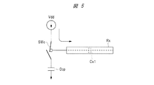
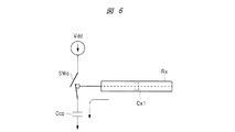
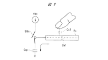
図5〜図8は、自己容量検出方式を説明するための図である。 5 to 8 are diagrams for explaining the self-capacitance detection method.
図5および図6は、表示装置DSPのタッチ検出面に、利用者の指が接触も近接もしていない状態を示している。このため、検出電極Rxと指との間に静電容量結合は生じていない。図5は、制御スイッチSWcにより、検出電極Rxが電源Vddに接続された状態を示す。図6は、制御スイッチSWcにより、検出電極Rxが電源Vddから遮断され、検出電極Rxがコンデンサとしての容量Ccpに接続された状態を示す。 5 and 6 show a state where the user's finger is not in contact with or close to the touch detection surface of the display device DSP. For this reason, no capacitive coupling occurs between the detection electrode Rx and the finger. FIG. 5 shows a state in which the detection electrode Rx is connected to the power supply Vdd by the control switch SWc. FIG. 6 shows a state in which the detection electrode Rx is disconnected from the power source Vdd by the control switch SWc, and the detection electrode Rx is connected to the capacitor Ccp as a capacitor.
図5の状態で、容量Cx1は例えば充電され、図6の状態で、容量Cx1は例えば放電される。ここで、容量Cx1が充電されることとは、検出電極Rxに対して書込み信号が書込まれることである。また、容量Cx1が放電されることとは、検出電極Rxに生じた静電容量の変化を示す読取り信号を読取ることである。 In the state of FIG. 5, the capacitor Cx1 is charged, for example, and in the state of FIG. 6, the capacitor Cx1 is discharged, for example. Here, the charging of the capacitor Cx1 means that a write signal is written to the detection electrode Rx. Further, the discharge of the capacitor Cx1 means reading a read signal indicating a change in capacitance generated in the detection electrode Rx.
一方、図7および図8は、表示装置DSPのタッチ検出面に、利用者の指が接触または近接している状態を示している。このため、検出電極Rxと指との間に静電容量結合が生じている。図7は、制御スイッチSWcにより、検出電極Rxが電源Vddに接続された状態を示す。図8は、制御スイッチSWcにより、検出電極Rxが電源Vddから遮断され、検出電極Rxが容量Ccpに接続された状態を示す。 On the other hand, FIGS. 7 and 8 show a state where the user's finger is in contact with or close to the touch detection surface of the display device DSP. For this reason, capacitive coupling is generated between the detection electrode Rx and the finger. FIG. 7 shows a state in which the detection electrode Rx is connected to the power supply Vdd by the control switch SWc. FIG. 8 shows a state where the detection electrode Rx is disconnected from the power source Vdd by the control switch SWc, and the detection electrode Rx is connected to the capacitor Ccp.
図7の状態で、容量Cx1は例えば充電され、図8の状態で、容量Cx1は例えば放電される。 In the state of FIG. 7, the capacitor Cx1 is charged, for example, and in the state of FIG. 8, the capacitor Cx1 is discharged, for example.
ここで、図6に示す放電時の容量Ccpの電圧の時間依存性に対して、図8に示す放電時の容量Ccpの電圧の時間依存性は、容量Cx2が存在するために、明らかに異なる。したがって、自己容量検出方式では、容量Ccpの電圧の時間依存性が、容量Cx2の有無により、異なることを利用して、入力位置情報(例えば、操作入力の有無)を判断している。 Here, the time dependency of the voltage of the capacitor Ccp at the time of discharge shown in FIG. 8 is obviously different from the time dependency of the voltage of the capacitor Ccp at the time of discharge shown in FIG. 6 due to the presence of the capacitor Cx2. . Therefore, in the self-capacitance detection method, the input position information (for example, presence / absence of operation input) is determined using the fact that the time dependency of the voltage of the capacitor Ccp varies depending on the presence / absence of the capacitor Cx2.
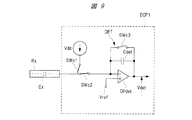
次に、自己容量検出方式を実現する回路の例について説明する。図9は、自己容量検出方式を実現する回路の一例を示す図である。なお、図9では、検出電極Rxの容量を容量Cxと表示している。 Next, an example of a circuit that realizes the self-capacitance detection method will be described. FIG. 9 is a diagram illustrating an example of a circuit that realizes the self-capacitance detection method. In FIG. 9, the capacitance of the detection electrode Rx is indicated as a capacitance Cx.
図9に示すような自己容量検出方式を実現する回路は、例えば図1に示した検出部SEに設けられている。あるいは、検出部SEが、例えば図1に示した駆動ICチップIC1内に設けられ、このような自己容量検出方式を実現する回路が、駆動ICチップIC1に設けられていてもよい。 A circuit that realizes the self-capacitance detection method as shown in FIG. 9 is provided in, for example, the detection unit SE shown in FIG. Alternatively, the detection unit SE may be provided in, for example, the drive IC chip IC1 illustrated in FIG. 1, and a circuit that realizes such a self-capacitance detection method may be provided in the drive IC chip IC1.
図9に示すように、検出電極Rxは、スイッチSWc1により、電源Vddに切り替え可能に接続されている。また、検出電極Rxは、スイッチSWc2により、積分回路としての電圧検出器DETに切り替え可能に接続されている。電圧検出器DETは、例えばオペアンプOPdetと、容量Cdetと、スイッチSWc3と、を含む。オペアンプOPdetには、参照信号Vrefが入力される。 As shown in FIG. 9, the detection electrode Rx is connected to the power source Vdd by a switch SWc1 so as to be switchable. The detection electrode Rx is switchably connected to a voltage detector DET as an integration circuit by a switch SWc2. The voltage detector DET includes, for example, an operational amplifier OPdet, a capacitor Cdet, and a switch SWc3. A reference signal Vref is input to the operational amplifier OPdet.
なお、図9では、図16を用いて説明する検出部SEに含まれる検出回路DCP1を図示している。 In FIG. 9, a detection circuit DCP1 included in the detection unit SE described with reference to FIG. 16 is illustrated.
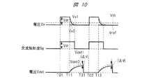
図10は、電源から出力される交流矩形波Sg、検出電極の電圧Vx、および、電圧検出器の出力としての電圧Vdetの時間依存性の例を模式的に示すグラフである。 FIG. 10 is a graph schematically showing an example of the time dependence of the AC rectangular wave Sg output from the power supply, the voltage Vx of the detection electrode, and the voltage Vdet as the output of the voltage detector.
図10に示すように、電源Vddは、時刻T01と時刻T02との時間差を周期とし、かつ、電圧Vdrの波形高さを有する交流矩形波Sgを出力する。交流矩形波Sgは、例えば数kHz〜数百kHz程度の周波数を有する。電圧検出器DETは、交流矩形波Sgに応じた電流の変動を電圧の変動(波形Vdet0および波形Vdet1)に変換する。 As shown in FIG. 10, the power supply Vdd outputs an AC rectangular wave Sg having a time difference between the time T01 and the time T02 as a cycle and having a waveform height of the voltage Vdr. The AC rectangular wave Sg has a frequency of about several kHz to several hundred kHz, for example. The voltage detector DET converts a current fluctuation according to the AC rectangular wave Sg into a voltage fluctuation (waveform Vdet0 and waveform Vdet1).
前述したように、検出電極Rxは、スイッチSWc1およびスイッチSWc2により、電源Vddおよび電圧検出器DETに、切り替え可能に接続されている。図10において、時刻T01のタイミングで交流矩形波Sgは電圧Vdr分だけ電圧を上昇させる。このとき、スイッチSWc1はオン状態にされ、スイッチSWc2はオフ状態にされている。このため、検出電極Rxの電圧Vxも電圧Vdr分だけ上昇する。次に、時刻T11のタイミングの前に、スイッチSWc1をオフ状態にする。このとき、検出電極Rxは電気的に浮遊した状態であるが、検出電極Rxの容量Cx1(図5参照)、あるいは検出電極Rxの容量Cx1に指等の接触または近接による容量Cx2を加えた容量Cx1+Cx2(図7参照)によって、検出電極Rxの電圧Vxの電圧Vdr分の上昇は維持される。さらに、時刻T11のタイミングの前にスイッチSWc3をオン状態にし、所定の時間経過後にスイッチSWc3をオフ状態にすることにより、電圧検出器DETをリセットさせる。このリセット動作により、電圧検出器DETの出力としての電圧Vdetは、参照信号Vrefと略等しい電圧となる。 As described above, the detection electrode Rx is switchably connected to the power source Vdd and the voltage detector DET by the switch SWc1 and the switch SWc2. In FIG. 10, the AC rectangular wave Sg increases the voltage by the voltage Vdr at time T01. At this time, the switch SWc1 is turned on and the switch SWc2 is turned off. For this reason, the voltage Vx of the detection electrode Rx also increases by the voltage Vdr. Next, the switch SWc1 is turned off before the time T11. At this time, although the detection electrode Rx is in an electrically floating state, the capacitance Cx1 (see FIG. 5) of the detection electrode Rx, or the capacitance obtained by adding the capacitance Cx2 due to contact or proximity of a finger or the like to the capacitance Cx1 of the detection electrode Rx. By Cx1 + Cx2 (see FIG. 7), the increase of the voltage Vx of the detection electrode Rx by the voltage Vdr is maintained. Further, the voltage detector DET is reset by turning on the switch SWc3 before the timing of the time T11 and turning off the switch SWc3 after a predetermined time has elapsed. By this reset operation, the voltage Vdet as the output of the voltage detector DET becomes substantially equal to the reference signal Vref.
続いて、時刻T11のタイミングでスイッチSWc2をオン状態にすると、電圧検出器DETの反転入力部に入力される電圧が検出電極Rxの電圧Vxに等しくなり、その後、検出電極Rxの容量Cx1(または容量Cx1+Cx2)と電圧検出器DETに含まれる容量Cdetに起因した時定数に従って、電圧検出器DETの反転入力部の電圧は、参照信号Vrefまで低下する。このとき、検出電極Rxの容量Cx1(または容量Cx1+Cx2)に蓄積されていた電荷が電圧検出器DETに含まれる容量Cdetに移動するため、電圧検出器DETの電圧Vdetが上昇する。検出電極Rxに指などの物体が近接も接触もしていないときは、電圧Vdetは、実線で示す波形Vdet0となり、Vdet=Cx1×Vdr/Cdetとなる。指などの物体が近接または接触してその物体の影響による容量が付加されたときは、電圧Vdetは、破線で示す波形Vdet1となり、Vdet=(Cx1+Cx2)×Vdr/Cdetとなる。 Subsequently, when the switch SWc2 is turned on at time T11, the voltage input to the inverting input portion of the voltage detector DET becomes equal to the voltage Vx of the detection electrode Rx, and then the capacitance Cx1 (or the detection electrode Rx) According to the time constant caused by the capacitance Cx1 + Cx2) and the capacitance Cdet included in the voltage detector DET, the voltage at the inverting input of the voltage detector DET drops to the reference signal Vref. At this time, since the charge accumulated in the capacitance Cx1 (or capacitance Cx1 + Cx2) of the detection electrode Rx moves to the capacitance Cdet included in the voltage detector DET, the voltage Vdet of the voltage detector DET increases. When an object such as a finger is not approaching or touching the detection electrode Rx, the voltage Vdet is a waveform Vdet0 indicated by a solid line, and Vdet = Cx1 × Vdr / Cdet. When an object such as a finger approaches or touches and a capacitance due to the influence of the object is added, the voltage Vdet becomes a waveform Vdet1 indicated by a broken line, and Vdet = (Cx1 + Cx2) × Vdr / Cdet.
その後、検出電極Rxの容量Cx1(または容量Cx1+Cx2)の電荷が容量Cdetに十分移動した後の時刻T31のタイミングでスイッチSWc2をオフ状態にし、スイッチSWc1およびスイッチSWc3をオン状態にすることにより、検出電極Rxの電圧を交流矩形波Sgのローレベルと等しい電圧にするとともに電圧検出器DETをリセットさせる。なお、このとき、スイッチSWc1をオン状態にするタイミングは、スイッチSWc2をオフ状態にした後、時刻T02以前であればいずれのタイミングでもよい。また、電圧検出器DETをリセットさせるタイミングは、スイッチSWc2をオフ状態にした後、時刻T12以前であればいずれのタイミングでもよい。以上の動作を所定の周波数(例えば数kHz〜数百kHz程度)で繰り返す。そして、波形Vdet0と波形Vdet1との差分の絶対値|ΔV|に基づいて、外部からタッチ検出面に近接または接触した物体の有無(タッチの有無)を測定することができる。 Thereafter, the switch SWc2 is turned off at the timing of time T31 after the charge of the capacitor Cx1 (or the capacitor Cx1 + Cx2) of the detection electrode Rx has sufficiently moved to the capacitor Cdet, and the switch SWc1 and the switch SWc3 are turned on. The voltage of the electrode Rx is set equal to the low level of the AC rectangular wave Sg and the voltage detector DET is reset. At this time, the timing for turning on the switch SWc1 may be any timing before the time T02 after the switch SWc2 is turned off. The timing of resetting the voltage detector DET may be any timing as long as it is before time T12 after the switch SWc2 is turned off. The above operation is repeated at a predetermined frequency (for example, about several kHz to several hundred kHz). Based on the absolute value | ΔV | of the difference between the waveform Vdet0 and the waveform Vdet1, it is possible to measure the presence / absence of an object that has approached or touched the touch detection surface from the outside (the presence or absence of a touch).
なお、指などの物体が近接も接触もしていないときは、検出電極Rxの電圧Vxの波形は、実線で示す波形Vx0となり、指などの物体が近接または接触してその物体の影響による容量Cx2が付加されたときは、検出電極Rxの電圧Vxの波形は、破線で示す波形Vx1となる。波形Vx0と波形Vx1とが、それぞれ所定の閾値電圧Vthまで下がる時間を測定することにより、外部からタッチ検出面に近接または接触した物体の有無(タッチの有無)を測定することもできる。 When an object such as a finger is not in proximity or contact, the waveform of the voltage Vx of the detection electrode Rx is a waveform Vx0 indicated by a solid line, and the capacitance Cx2 due to the influence of the object such as a finger approaching or contacting Is added, the waveform of the voltage Vx of the detection electrode Rx is a waveform Vx1 indicated by a broken line. By measuring the time when each of the waveform Vx0 and the waveform Vx1 decreases to the predetermined threshold voltage Vth, it is possible to measure the presence / absence of an object that has approached or touched the touch detection surface from the outside (presence / absence of touch).
あるいは、自己容量検出方式を実現する回路として別の例を用いてもよい。図11は、自己容量検出方式を実現する回路の別の例を示す図である。 Or you may use another example as a circuit which implement | achieves a self-capacitance detection system. FIG. 11 is a diagram illustrating another example of a circuit that realizes the self-capacitance detection method.
図11に示すような自己容量検出方式を実現する回路は、例えば図1に示した検出部SEに設けられている。あるいは、検出部SEが、例えば図1に示した駆動ICチップIC1内に設けられ、このような自己容量検出方式を実現する回路が、駆動ICチップIC1に設けられていてもよい。 A circuit that realizes the self-capacitance detection method as shown in FIG. 11 is provided in, for example, the detection unit SE shown in FIG. Alternatively, the detection unit SE may be provided in, for example, the drive IC chip IC1 illustrated in FIG. 1, and a circuit that realizes such a self-capacitance detection method may be provided in the drive IC chip IC1.
図11に示すように、検出電極Rxは、積分回路としての電圧検出器DETに接続されている。電圧検出器DETは、例えばオペアンプOPdetと、容量Cdetと、スイッチSWc3と、を含む。オペアンプOPdetの2つの入力端子のうち、「+」により表された非反転入力端子には、検出電極Rxが接続されており、「−」により表された反転入力端子には、交流矩形波Sgが入力される。また、オペアンプOPdetでは、反転入力端子と非反転入力端子とが仮想的に短絡、すなわちイマジナリショートされている。検出電極Rxが検出回路DCP1に接続されるとき、スイッチSWc3はオフ状態(非導通状態)にされ、検出電極Rxが検出回路DCP1に接続されないとき、スイッチSWc3はオン状態(導通状態)にされる。 As shown in FIG. 11, the detection electrode Rx is connected to a voltage detector DET as an integration circuit. The voltage detector DET includes, for example, an operational amplifier OPdet, a capacitor Cdet, and a switch SWc3. Of the two input terminals of the operational amplifier OPdet, the detection electrode Rx is connected to the non-inverting input terminal represented by “+”, and the AC rectangular wave Sg is connected to the inverting input terminal represented by “−”. Is entered. In the operational amplifier OPdet, the inverting input terminal and the non-inverting input terminal are virtually short-circuited, that is, imaginary short-circuited. When the detection electrode Rx is connected to the detection circuit DCP1, the switch SWc3 is turned off (non-conductive state), and when the detection electrode Rx is not connected to the detection circuit DCP1, the switch SWc3 is turned on (conductive state). .
なお、図11では、図16を用いて説明する検出部SEに含まれる検出回路DCP1を図示している。 FIG. 11 illustrates a detection circuit DCP1 included in the detection unit SE described with reference to FIG.
図12は、交流矩形波Sg、および、電圧検出器の出力としての電圧Vdetの時間依存性の例を模式的に示すグラフである。 FIG. 12 is a graph schematically showing an example of time dependence of the AC rectangular wave Sg and the voltage Vdet as the output of the voltage detector.
図12に示すように、交流矩形波Sgは、電圧Vdrの波形高さを有する。前述したように、オペアンプOPdetは、イマジナリショートされているため、オペアンプOPdetの反転入力端子に交流矩形波Sgが入力されると、オペアンプOPdetの非反転入力端子に接続された検出電極Rxには、交流矩形波Sgと同電位の駆動信号が印加される。 As shown in FIG. 12, the AC rectangular wave Sg has a waveform height of the voltage Vdr. As described above, since the operational amplifier OPdet is imaginarily short-circuited, when the AC rectangular wave Sg is input to the inverting input terminal of the operational amplifier OPdet, the detection electrode Rx connected to the non-inverting input terminal of the operational amplifier OPdet A drive signal having the same potential as that of the AC rectangular wave Sg is applied.
一方、検出電極Rxは容量Cxを有するため、検出電極Rxの電位と駆動信号との間には差分の電圧が発生し、この差分の電圧に相当する電流が検出電極RxとオペアンプOPdetの非反転入力端子との間で流れることになる。電圧検出器DETからは、この電流を電圧検出器DETにより電圧に変換して積分した値が、波形Vdet0を有する電圧Vdetとして出力される。電圧Vdetの波形Vdet0は、図12において、実線で示されている。 On the other hand, since the detection electrode Rx has a capacitance Cx, a difference voltage is generated between the potential of the detection electrode Rx and the drive signal, and a current corresponding to the difference voltage is non-inverted between the detection electrode Rx and the operational amplifier OPdet. It flows between the input terminals. From the voltage detector DET, a value obtained by converting this current into a voltage by the voltage detector DET and integrating the voltage is output as a voltage Vdet having a waveform Vdet0. A waveform Vdet0 of the voltage Vdet is indicated by a solid line in FIG.
検出電極Rxに指などの物体が近接または接触すると、容量Cxが増加するため、検出電極Rxの電位と駆動信号との間に発生する差分の電圧が増加し、この差分の電圧に相当し、検出電極RxとオペアンプOPdetの非反転入力端子との間で流れる電流が増加する。そのため、この電流を電圧検出器DETにより電圧に変換して積分した値が増加し、電圧検出器DETから出力される電圧Vdetの波形Vdet1の変化は、波形Vdet0の変化に比べて増加する。波形Vdet1は、図12において、破線で示されている。 When an object such as a finger approaches or comes into contact with the detection electrode Rx, the capacitance Cx increases, so that a differential voltage generated between the potential of the detection electrode Rx and the drive signal increases, which corresponds to this differential voltage, The current flowing between the detection electrode Rx and the non-inverting input terminal of the operational amplifier OPdet increases. For this reason, the value obtained by converting this current into a voltage by the voltage detector DET and integrated increases, and the change in the waveform Vdet1 of the voltage Vdet output from the voltage detector DET increases compared to the change in the waveform Vdet0. The waveform Vdet1 is indicated by a broken line in FIG.
したがって、電圧検出器DETから出力された電圧Vdetを所定の閾値電圧と比較することにより、検出電極Rxへの指などの近接または接触の有無を検出することができる。すなわち、波形Vdet0と波形Vdet1との差分の絶対値|ΔV|に基づいて、外部からタッチ検出面に近接または接触した物体の有無(タッチの有無)を測定することができる。なお、電圧検出器DETの動作は、絶対値|ΔV|を精度よく検出するため、例えばスイッチSWc3により、交流矩形波Sgの周波数に合わせて、容量Cdetの充放電をリセットする期間Resetを設けた動作としてもよい。 Therefore, by comparing the voltage Vdet output from the voltage detector DET with a predetermined threshold voltage, it is possible to detect the proximity or contact of a finger or the like to the detection electrode Rx. That is, based on the absolute value | ΔV | of the difference between the waveform Vdet0 and the waveform Vdet1, it is possible to measure the presence / absence of an object that has approached or touched the touch detection surface from the outside (presence / absence of touch). In the operation of the voltage detector DET, in order to detect the absolute value | ΔV | with high accuracy, a period Reset for resetting charging / discharging of the capacitor Cdet is provided by the switch SWc3 in accordance with the frequency of the AC rectangular wave Sg. It is good also as operation.
このような、図11および図12を用いて説明した検出方法は、図9および図10を用いて説明した検出方法と異なり、スイッチSWc1およびSWc2のいずれも不要であり、駆動信号としての交流矩形波Sgを、直接オペアンプOPdetに供給する方法である。 The detection method described with reference to FIGS. 11 and 12 is different from the detection method described with reference to FIGS. 9 and 10, and neither of the switches SWc1 and SWc2 is required, and an AC rectangle as a drive signal is used. In this method, the wave Sg is directly supplied to the operational amplifier OPdet.
なお、図11に示す検出回路DCP1は、自己容量検出方式および相互容量検出方式のいずれにも兼用することができる。図11に示す検出回路DCP1を相互容量検出方式に用いる場合には、オペアンプOPdetの反転入力端子が、交流矩形波Sgを供給する供給回路に代えて、固定電位としての参照信号を供給する供給回路に接続されるように、接続を切り替えればよい。 Note that the detection circuit DCP1 shown in FIG. 11 can be used for both the self-capacitance detection method and the mutual capacitance detection method. When the detection circuit DCP1 shown in FIG. 11 is used in the mutual capacitance detection method, the inverting input terminal of the operational amplifier OPdet replaces the supply circuit that supplies the AC rectangular wave Sg and supplies a reference signal as a fixed potential. The connection may be switched so that the connection is established.
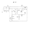
あるいは、自己容量検出方式を実現する回路としてさらに別の例を用いてもよい。図13は、自己容量検出方式を実現する回路のさらに別の例を示す図である。 Alternatively, another example may be used as a circuit that realizes the self-capacitance detection method. FIG. 13 is a diagram illustrating still another example of a circuit that realizes the self-capacitance detection method.
図13に示す例では、検出電極Rxは、分圧用の容量Cpの一方の端子に接続されるとともに、比較器COMPの一方の入力端子に接続される。検出電極Rxは、自己の容量Cxを有する。比較器COMPの他方の入力端子には、参照信号Vrefの供給端子が接続されている。 In the example shown in FIG. 13, the detection electrode Rx is connected to one terminal of the voltage dividing capacitor Cp and to one input terminal of the comparator COMP. The detection electrode Rx has its own capacitance Cx. A supply terminal for the reference signal Vref is connected to the other input terminal of the comparator COMP.
容量Cpの他方の端子は、スイッチSW1を介して電圧Vccの電源配線に接続される。また容量Cpの他方の端子は、抵抗Rcを介して容量Ccの一方の端子に接続されている。容量Ccの他方の端子は、基準電位(例えばアース電位)に接続されている。 The other terminal of the capacitor Cp is connected to the power supply wiring of the voltage Vcc through the switch SW1. The other terminal of the capacitor Cp is connected to one terminal of the capacitor Cc via the resistor Rc. The other terminal of the capacitor Cc is connected to a reference potential (for example, ground potential).
スイッチSW2は、容量Cpの他方の端子と基準電位間に接続され、スイッチSW3は、容量Cpの一方の端子と基準電位間に接続されている。スイッチSW1、SW2およびSW3ならびに比較器COMPは、例えば図1に示した検出部SEに設けられている。 The switch SW2 is connected between the other terminal of the capacitor Cp and the reference potential, and the switch SW3 is connected between one terminal of the capacitor Cp and the reference potential. The switches SW1, SW2 and SW3 and the comparator COMP are provided, for example, in the detection unit SE shown in FIG.
なお、図13では、図16を用いて説明する検出部SEに含まれる検出回路DCP1を図示している。 Note that FIG. 13 illustrates a detection circuit DCP1 included in the detection unit SE described with reference to FIG.
図13に示す例では、スイッチSW1は、一定の周期でオン状態(導通状態)にされ、このオン状態のときに容量Ccを充電することができる。容量Ccが充電されるときは、スイッチSW2およびSW3はオフ状態にされている。容量Ccが充電されると、スイッチSW1、SW2およびSW3が全てオフ状態にされ、容量Ccの電荷が保持される。 In the example shown in FIG. 13, the switch SW1 is turned on (conductive state) at a constant cycle, and the capacitor Cc can be charged in this on state. When the capacitor Cc is charged, the switches SW2 and SW3 are turned off. When the capacitor Cc is charged, the switches SW1, SW2 and SW3 are all turned off, and the charge of the capacitor Cc is held.
続いて、スイッチSW1のオフ状態を維持したまま、スイッチSW2およびSW3が一定時間オン状態にされる。すると、容量CpおよびCxの電荷のほとんどが放電されるとともに、容量Ccの電荷の一部が、抵抗Rcを介して放電される。 Subsequently, the switches SW2 and SW3 are turned on for a predetermined time while the switch SW1 is kept off. Then, most of the charges in the capacitors Cp and Cx are discharged, and part of the charge in the capacitor Cc is discharged through the resistor Rc.
次いで、スイッチSW1、SW2およびSW3が全てオフ状態にされる。すると、容量Ccの電荷が、容量CpおよびCxに移動する。そして、容量Cxの電圧Vxが比較器COMPにおいて、参照信号Vrefまたは閾値電圧Vthと比較される。 Next, the switches SW1, SW2 and SW3 are all turned off. Then, the charge of the capacitor Cc moves to the capacitors Cp and Cx. Then, the voltage Vx of the capacitor Cx is compared with the reference signal Vref or the threshold voltage Vth in the comparator COMP.
容量Ccの電圧を電圧Vcとし、容量Cpの電圧を電圧Vpとする。このとき、電圧Vxは、電圧Vcと電圧Vpとの和に等しく、電圧Vcの変化の特性または変換の度合いは、容量Cpと容量Cxの合計値に応じて変化する。容量Cxの変化は、容量Cxの電圧Vxに対しても影響を与える。また、容量Cxの値は、検出電極Rxに対する利用者の指の接近の程度に応じて異なる。 The voltage of the capacitor Cc is set as the voltage Vc, and the voltage of the capacitor Cp is set as the voltage Vp. At this time, the voltage Vx is equal to the sum of the voltage Vc and the voltage Vp, and the change characteristic or the degree of conversion of the voltage Vc changes according to the total value of the capacitance Cp and the capacitance Cx. The change in the capacitance Cx also affects the voltage Vx of the capacitance Cx. Further, the value of the capacitance Cx varies depending on the degree of approach of the user's finger to the detection electrode Rx.
このため、指が検出電極Rxから遠い場合は、電圧Vcの時間依存性は、ゆっくりした変化を伴う特性となり、指が検出電極Rxに近い場合は、電圧Vcの時間依存性は、すばやい変化を伴う特性となる。 For this reason, when the finger is far from the detection electrode Rx, the time dependency of the voltage Vc has a characteristic with a slow change, and when the finger is close to the detection electrode Rx, the time dependency of the voltage Vc changes quickly. Accompanying characteristics.
比較器COMPは、スイッチSW2およびSW3のオン状態とオフ状態とが繰り返されるのに同期して、電圧Vxを参照信号Vrefまたは閾値電圧Vthと比較する。そしてVx>Vrefのときは、比較器COMPは、出力パルスを得る。しかし比較器COMPは、Vx<Vrefになると出力パルスを停止する。 The comparator COMP compares the voltage Vx with the reference signal Vref or the threshold voltage Vth in synchronization with the ON state and the OFF state of the switches SW2 and SW3 being repeated. When Vx> Vref, the comparator COMP obtains an output pulse. However, the comparator COMP stops the output pulse when Vx <Vref.
このとき、比較器COMPの出力パルスが得られる期間が計測されてもよいし、比較器COMPの出力パルス数(容量Ccの充電後、Vx<Vrefになるまでのパルス数)が計測されてもよい。 At this time, the period during which the output pulse of the comparator COMP is obtained may be measured, or the number of output pulses of the comparator COMP (the number of pulses until Vx <Vref after charging the capacitor Cc) may be measured. Good.
このように、図13を用いて説明した方法によっても、検出面に対する指の近接または接触の程度を比較器COMPの出力パルスの状態で判断することができる。 As described above, also by the method described with reference to FIG. 13, the degree of proximity or contact of the finger to the detection surface can be determined from the state of the output pulse of the comparator COMP.
<タッチ検出方法およびタッチ検出回路>
次に、本実施の形態1の表示装置におけるタッチ検出方法およびタッチ検出回路について説明する。
<Touch detection method and touch detection circuit>
Next, a touch detection method and a touch detection circuit in the display device according to the first embodiment will be described.
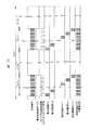
初めに、本実施の形態1の表示装置におけるタッチ検出方法について説明する。図14は、実施の形態1の表示装置におけるタッチ検出方法を説明するための図である。図15は、実施の形態1の表示装置におけるタッチ検出方法を説明するためのフロー図である。なお、図14においてハッチングを付した部分である領域AR1は、領域AR1を拡大して領域AR2として示すように、例えば矩形波を有する駆動信号が検出回路DCP1により供給されている部分である。 First, a touch detection method in the display device according to the first embodiment will be described. FIG. 14 is a diagram for explaining a touch detection method in the display device according to the first embodiment. FIG. 15 is a flowchart for explaining the touch detection method in the display device according to the first embodiment. In FIG. 14, the area AR1 that is a hatched part is a part to which, for example, a drive signal having a rectangular wave is supplied by the detection circuit DCP1, as shown in the area AR2 by enlarging the area AR1.
本実施の形態1の表示装置は、タッチ検出機能を有する検出部SE(図1参照)を有する。そして、図14および図15に示すように、本実施の形態1の表示装置では、検出部SEは、指の近接または接触を検出する指近接検出処理としてのステップS1と、近接または接触した指の座標を検出する指座標検出処理としてのステップS2と、を行う。 The display device according to the first embodiment includes a detection unit SE (see FIG. 1) having a touch detection function. As shown in FIGS. 14 and 15, in the display device according to the first embodiment, the detection unit SE performs step S1 as finger proximity detection processing for detecting the proximity or contact of the finger, and the finger that is in proximity or contact. Step S2 is performed as finger coordinate detection processing for detecting the coordinates.
ここで、指近接検出処理としてのステップS1を待機モードと称し、指座標検出処理としてのステップS2を検出モードと称する場合、検出部SEは、検出モードとしての指座標検出処理の前に、待機モードとしての指近接検出処理を行うことになる。 Here, when step S1 as the finger proximity detection process is referred to as a standby mode and step S2 as the finger coordinate detection process is referred to as a detection mode, the detection unit SE waits before the finger coordinate detection process as the detection mode. Finger proximity detection processing as a mode is performed.
ステップS1では、検出部SEは、まず、シールド電極SHを検出する(図15のステップS11)。このステップS11では、検出部SEは、一体として形成された1個のシールド電極SHの静電容量の変化を検出することにより、上側からのタッチ検出面TDSへの指などの物体の近接または接触を検出する。言い換えれば、ステップS11では、シールド電極SHの静電容量の変化に基づいて、第1の側(図3中上側)からの表示パネルPNLの前面FSへの物体の近接または接触が検出される。 In step S1, the detection unit SE first detects the shield electrode SH (step S11 in FIG. 15). In step S11, the detection unit SE detects a change in the capacitance of one shield electrode SH formed as a single unit, thereby approaching or touching an object such as a finger from the upper side to the touch detection surface TDS. Is detected. In other words, in step S11, the proximity or contact of an object from the first side (upper side in FIG. 3) to the front surface FS of the display panel PNL is detected based on the change in the capacitance of the shield electrode SH.
ステップS1では、検出部SEは、次に、物体の近接が検出されたか判定する(図15のステップS12)。このステップS12では、検出部SEは、タッチ検出面TDSへの指などの物体の近接または接触が検出されたか判定する。ステップS12において、指などの物体の近接または接触が検出されなかったと判定されたとき、検出部SEは、しばらく待つ(図15のステップS13)。そして、検出部SEは、ステップS13を行ってしばらく待った後、ステップS11を再び繰り返す。一方、ステップS12において、指などの物体の近接または接触が検出されたと判定されたとき、検出部SEは、ステップS2を行う。 In step S1, the detection unit SE next determines whether proximity of an object has been detected (step S12 in FIG. 15). In step S12, the detection unit SE determines whether the proximity or contact of an object such as a finger to the touch detection surface TDS has been detected. When it is determined in step S12 that the proximity or contact of an object such as a finger has not been detected, the detection unit SE waits for a while (step S13 in FIG. 15). Then, the detection unit SE performs step S13 and waits for a while, and then repeats step S11 again. On the other hand, when it is determined in step S12 that the proximity or contact of an object such as a finger has been detected, the detection unit SE performs step S2.
ステップS2では、まず、検出部SEは、各検出電極Rxを個別に検出する(図15のステップS21)。このステップS21では、検出部SEは、複数の検出電極Rxの各々の静電容量の変化を個別に検出することにより、タッチ検出面TDSでの指などの物体の位置、すなわち座標を検出する。言い換えれば、ステップS21では、複数の検出電極Rxの各々の静電容量の変化に基づいて、第1の側(図3中上側)から前面FSに近接または接触した物体の位置が検出される。 In step S2, the detection unit SE first detects each detection electrode Rx individually (step S21 in FIG. 15). In step S21, the detection unit SE detects the position, that is, the coordinates of an object such as a finger on the touch detection surface TDS by individually detecting the change in capacitance of each of the plurality of detection electrodes Rx. In other words, in step S21, the position of an object that has approached or contacted the front surface FS from the first side (upper side in FIG. 3) is detected based on the change in capacitance of each of the plurality of detection electrodes Rx.
ステップS2では、次に、検出部SEは、物体の座標が検出されたか判定する(図15のステップS22)。このステップS22では、タッチ検出面TDSでの指などの物体の座標が検出されたか判定する。ステップS22において、指などの物体の座標が検出されたときは、検出部SEは、ステップS21を再び繰り返す。一方、ステップS22において、指などの物体の座標が検出されなかった場合には、検出部SEは、ステップS1、すなわちステップS11を再び行う。 Next, in step S2, the detection unit SE determines whether the coordinates of the object have been detected (step S22 in FIG. 15). In step S22, it is determined whether the coordinates of an object such as a finger on the touch detection surface TDS have been detected. When the coordinates of an object such as a finger are detected in step S22, the detection unit SE repeats step S21 again. On the other hand, if the coordinates of an object such as a finger are not detected in step S22, the detection unit SE performs step S1, that is, step S11 again.
なお、図14では、ステップS11において、一体として形成された1個のシールド電極SHの静電容量の変化を検出する場合を示している。しかし、後述する図24を用いて説明するように、分割して形成された複数個のシールド電極SHの各々の静電容量の変化を検出してもよい。 FIG. 14 shows a case where a change in the capacitance of one shield electrode SH formed integrally is detected in step S11. However, as will be described later with reference to FIG. 24, a change in electrostatic capacitance of each of the plurality of shield electrodes SH formed by division may be detected.
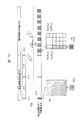
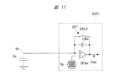
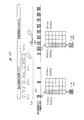
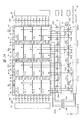
次に、図16〜図18を参照し、本実施の形態1の表示装置におけるタッチ検出回路について説明する。図16は、実施の形態1の表示装置におけるタッチ検出回路を示す図である。図17および図18は、シールド電極を用いたタッチ検出を説明するための図である。図16は、シールド電極SHにハッチングを付すことにより、ステップS11において、シールド電極SHが検出回路DCP2と接続されている状態を示している。図17は、表示装置のタッチ検出面に、指などの物体が接触も近接もしていない状態を示している。図18は、表示装置のタッチ検出面に、指などの物体が接触または近接している状態を示している。 Next, a touch detection circuit in the display device according to the first embodiment will be described with reference to FIGS. FIG. 16 is a diagram illustrating a touch detection circuit in the display device according to the first embodiment. 17 and 18 are diagrams for explaining touch detection using a shield electrode. FIG. 16 shows a state where the shield electrode SH is connected to the detection circuit DCP2 in step S11 by hatching the shield electrode SH. FIG. 17 illustrates a state in which an object such as a finger is not in contact with or close to the touch detection surface of the display device. FIG. 18 illustrates a state where an object such as a finger is in contact with or close to the touch detection surface of the display device.
なお、図17および図18では、シールド電極SHが、積分回路としての電圧検出器DETに接続されている。電圧検出器DETは、例えば図11を用いて説明した検出回路DCP1と同様の例であり、例えば電圧検出器DETは、オペアンプOPdet、容量CdetおよびスイッチSWc3を含む。オペアンプOPdetには、交流矩形波Sgが入力される。 In FIG. 17 and FIG. 18, the shield electrode SH is connected to a voltage detector DET as an integrating circuit. The voltage detector DET is an example similar to the detection circuit DCP1 described with reference to FIG. 11, for example, and the voltage detector DET includes, for example, an operational amplifier OPdet, a capacitor Cdet, and a switch SWc3. An AC rectangular wave Sg is input to the operational amplifier OPdet.
図16に示すように、タッチ検出回路としての検出部SEは、検出回路DCP1およびDCP2と、接続回路CNC1およびCNC2と、ガード信号供給回路GSC1と、を含む。検出回路DCP1は、複数の検出電極Rxの各々の静電容量の変化を検出する。検出回路DCP2は、シールド電極SHの静電容量の変化を検出する。接続回路CNC1は、複数の検出電極Rxの各々を検出回路DCP1に切り替え可能に接続し、接続回路CNC2は、シールド電極SHを検出回路DCP2に切り替え可能に接続する。なお、図16に示すように、シールド電極SHは、平面視において複数の検出電極Rxの各々と重なり、シールド電極SHは、平面視において複数の走査線および信号線の各々と重なる。また、接続回路CNC1は、検出回路DCP1と複数の検出電極Rxとの接続状態を切り替える切り替え部である。 As shown in FIG. 16, the detection unit SE as a touch detection circuit includes detection circuits DCP1 and DCP2, connection circuits CNC1 and CNC2, and a guard signal supply circuit GSC1. The detection circuit DCP1 detects a change in capacitance of each of the plurality of detection electrodes Rx. The detection circuit DCP2 detects a change in the capacitance of the shield electrode SH. The connection circuit CNC1 connects each of the plurality of detection electrodes Rx to the detection circuit DCP1 in a switchable manner, and the connection circuit CNC2 connects the shield electrode SH to the detection circuit DCP2 in a switchable manner. As shown in FIG. 16, the shield electrode SH overlaps each of the plurality of detection electrodes Rx in a plan view, and the shield electrode SH overlaps each of the plurality of scanning lines and signal lines in the plan view. The connection circuit CNC1 is a switching unit that switches a connection state between the detection circuit DCP1 and the plurality of detection electrodes Rx.
なお、図16に示す例では、検出回路DCP1と検出回路DCP2とを一体化して示しているが、検出回路DCP2が設けられず、検出回路DCP1が、シールド電極SHの静電容量の変化を検出してもよい。また、接続回路CNC2が接続回路CNC1と一体的に設けられてもよく、接続回路CNC2が設けられず、接続回路CNC1がシールド電極SHを検出回路DCP2に切り替え可能に接続してもよい。 In the example shown in FIG. 16, the detection circuit DCP1 and the detection circuit DCP2 are shown as being integrated, but the detection circuit DCP2 is not provided, and the detection circuit DCP1 detects a change in the capacitance of the shield electrode SH. May be. Further, the connection circuit CNC2 may be provided integrally with the connection circuit CNC1, or the connection circuit CNC2 may not be provided, and the connection circuit CNC1 may connect the shield electrode SH to the detection circuit DCP2 in a switchable manner.
平面視においてY軸方向に配列された複数の検出電極Rxからなる電極群を、電極群RGと称する。このとき、表示装置は、複数の電極群RGを有する。複数の電極群RGは、平面視においてX軸方向に配列され、複数の電極群RGの各々は、平面視においてY軸方向に配列された複数の検出電極Rxを有する。 An electrode group composed of a plurality of detection electrodes Rx arranged in the Y-axis direction in plan view is referred to as an electrode group RG. At this time, the display device has a plurality of electrode groups RG. The plurality of electrode groups RG are arranged in the X-axis direction in plan view, and each of the plurality of electrode groups RG has a plurality of detection electrodes Rx arranged in the Y-axis direction in plan view.
図16に示す例では、電極群RGとして、検出電極Rx11、Rx12、Rx13およびRx14からなる電極群RG1、ならびに、検出電極Rx21、Rx22、Rx23およびRx24からなる電極群RG2が、設けられている。また、電極群RGとして、検出電極Rx31、Rx32、Rx33およびRx34からなる電極群RG3、ならびに、検出電極Rx41、Rx42、Rx43およびRx44からなる電極群RG4が、設けられている。すなわち、電極群RG1は、複数の検出電極Rx1を含み、電極群RG2は、複数の検出電極Rx2を含み、電極群RG3は、複数の検出電極Rx3を含み、電極群RG4は、複数の検出電極Rx4を含む。 In the example shown in FIG. 16, as the electrode group RG, an electrode group RG1 including detection electrodes Rx11, Rx12, Rx13, and Rx14, and an electrode group RG2 including detection electrodes Rx21, Rx22, Rx23, and Rx24 are provided. Further, as the electrode group RG, an electrode group RG3 composed of detection electrodes Rx31, Rx32, Rx33 and Rx34, and an electrode group RG4 composed of detection electrodes Rx41, Rx42, Rx43 and Rx44 are provided. That is, the electrode group RG1 includes a plurality of detection electrodes Rx1, the electrode group RG2 includes a plurality of detection electrodes Rx2, the electrode group RG3 includes a plurality of detection electrodes Rx3, and the electrode group RG4 includes a plurality of detection electrodes. Includes Rx4.
好適には、接続回路CNC1は、複数の電極群RGの各々を検出回路DCP1にそれぞれ接続する複数のトランジスタ群TGを含む。複数のトランジスタ群TGの各々は、複数のトランジスタTdを含む。複数のトランジスタTdの各々は、スイッチング素子としての電界トランジスタであり、複数のトランジスタTdの各々は、ゲート電極を含む。電極群RGとトランジスタ群TGとの組において、トランジスタ群TGに含まれる複数のトランジスタTdは、電極群RGに含まれる複数の検出電極Rxの各々を、検出回路DCP1にそれぞれ接続する。 Preferably, the connection circuit CNC1 includes a plurality of transistor groups TG that connect each of the plurality of electrode groups RG to the detection circuit DCP1. Each of the plurality of transistor groups TG includes a plurality of transistors Td. Each of the plurality of transistors Td is an electric field transistor as a switching element, and each of the plurality of transistors Td includes a gate electrode. In the set of the electrode group RG and the transistor group TG, the plurality of transistors Td included in the transistor group TG connect each of the plurality of detection electrodes Rx included in the electrode group RG to the detection circuit DCP1.
図16に示す例では、接続回路CNC1は、トランジスタTdとして、トランジスタ群TG1に含まれるトランジスタTd11、Td12、Td13およびTd14、ならびに、トランジスタ群TG2に含まれるTd21、Td22、Td23およびTd24を含む。また、接続回路CNC1は、トランジスタTdとして、トランジスタ群TG3に含まれるトランジスタTd31、Td32、Td33およびTd34、ならびに、トランジスタ群TG4に含まれるトランジスタTd41、Td42、Td43およびTd44を含む。 In the example shown in FIG. 16, the connection circuit CNC1 includes transistors Td11, Td12, Td13, and Td14 included in the transistor group TG1, and Td21, Td22, Td23, and Td24 included in the transistor group TG2 as the transistor Td. The connection circuit CNC1 includes transistors Td31, Td32, Td33, and Td34 included in the transistor group TG3, and transistors Td41, Td42, Td43, and Td44 included in the transistor group TG4 as the transistor Td.
トランジスタTd11は、検出電極Rx11を検出回路DCP1に接続し、トランジスタTd12は、検出電極Rx12を検出回路DCP1に接続し、トランジスタTd13は、検出電極Rx13を検出回路DCP1に接続し、トランジスタTd14は、検出電極Rx14を検出回路DCP1に接続する。トランジスタTd21は、検出電極Rx21を検出回路DCP1に接続し、トランジスタTd22は、検出電極Rx22を検出回路DCP1に接続し、トランジスタTd23は、検出電極Rx23を検出回路DCP1に接続し、トランジスタTd24は、検出電極Rx24を検出回路DCP1に接続する。 The transistor Td11 connects the detection electrode Rx11 to the detection circuit DCP1, the transistor Td12 connects the detection electrode Rx12 to the detection circuit DCP1, the transistor Td13 connects the detection electrode Rx13 to the detection circuit DCP1, and the transistor Td14 The electrode Rx14 is connected to the detection circuit DCP1. The transistor Td21 connects the detection electrode Rx21 to the detection circuit DCP1, the transistor Td22 connects the detection electrode Rx22 to the detection circuit DCP1, the transistor Td23 connects the detection electrode Rx23 to the detection circuit DCP1, and the transistor Td24 The electrode Rx24 is connected to the detection circuit DCP1.
トランジスタTd31は、検出電極Rx31を検出回路DCP1に接続し、トランジスタTd32は、検出電極Rx32を検出回路DCP1に接続し、トランジスタTd33は、検出電極Rx33を検出回路DCP1に接続し、トランジスタTd34は、検出電極Rx34を検出回路DCP1に接続する。トランジスタTd41は、検出電極Rx41を検出回路DCP1に接続し、トランジスタTd42は、検出電極Rx42を検出回路DCP1に接続し、トランジスタTd43は、検出電極Rx43を検出回路DCP1に接続し、トランジスタTd44は、検出電極Rx44を検出回路DCP1に接続する。 The transistor Td31 connects the detection electrode Rx31 to the detection circuit DCP1, the transistor Td32 connects the detection electrode Rx32 to the detection circuit DCP1, the transistor Td33 connects the detection electrode Rx33 to the detection circuit DCP1, and the transistor Td34 The electrode Rx34 is connected to the detection circuit DCP1. The transistor Td41 connects the detection electrode Rx41 to the detection circuit DCP1, the transistor Td42 connects the detection electrode Rx42 to the detection circuit DCP1, the transistor Td43 connects the detection electrode Rx43 to the detection circuit DCP1, and the transistor Td44 The electrode Rx44 is connected to the detection circuit DCP1.
また、好適には、検出部SEは、電圧供給回路VSC1およびVSC2と、クロック信号供給回路CLC1と、を含む。 Preferably, the detection unit SE includes voltage supply circuits VSC1 and VSC2, and a clock signal supply circuit CLC1.
電圧供給回路VSC1は、複数のトランジスタ群TGの各々に、トランジスタTdのゲート電圧である電圧V1を供給する。すなわち、電圧供給回路VSC1は、複数のトランジスタ群TGの各々に含まれる複数のトランジスタTdの各々のゲート電極に、電圧V1としての電圧V11または電圧V12を供給する。トランジスタTdは、ゲート電極に電圧V11が入力されているときに、オン状態(導通状態)であり、ゲート電極に電圧V12が入力されているときに、オフ状態(非導通状態)である。 The voltage supply circuit VSC1 supplies a voltage V1 that is a gate voltage of the transistor Td to each of the plurality of transistor groups TG. That is, the voltage supply circuit VSC1 supplies the voltage V11 or the voltage V12 as the voltage V1 to each gate electrode of the plurality of transistors Td included in each of the plurality of transistor groups TG. The transistor Td is in an on state (conductive state) when the voltage V11 is input to the gate electrode, and is in an off state (non-conductive state) when the voltage V12 is input to the gate electrode.
なお、電圧供給回路VSC1として、例えばシフトレジスタ回路、マルチプレクサ回路またはデコーダ回路など各種の回路を用いることができる。 As the voltage supply circuit VSC1, various circuits such as a shift register circuit, a multiplexer circuit, or a decoder circuit can be used.
ガード信号供給回路GSC1は、ステップS21において、複数の検出電極Rxの各々の静電容量の変化が、シールド電極SHからの影響を受けないようにするためのガード信号としての信号G1を、シールド電極SHに供給する。接続回路CNC2は、シールド電極SHを、検出回路DCP2またはガード信号供給回路GSC1に切り替えて接続する。 In step S21, the guard signal supply circuit GSC1 outputs a signal G1 as a guard signal for preventing changes in capacitance of each of the plurality of detection electrodes Rx from being affected by the shield electrode SH. Supply to SH. The connection circuit CNC2 switches and connects the shield electrode SH to the detection circuit DCP2 or the guard signal supply circuit GSC1.
図16に示す例では、接続回路CNC2は、電界効果トランジスタとしてのスイッチング素子CSWを1個含む。1個のスイッチング素子CSWは、シールド電極SHを、検出回路DCP2に接続する。 In the example shown in FIG. 16, the connection circuit CNC2 includes one switching element CSW as a field effect transistor. One switching element CSW connects the shield electrode SH to the detection circuit DCP2.
表示装置DSPは、複数の走査線GLと、走査線駆動回路GDと、信号線駆動回路SDと、切り替え部GSPおよびSSP1と、を有する。複数の走査線GLは、平面視において、複数の電極群RG、すなわち複数の検出電極Rxと重なる。複数の信号線SLは、平面視において、複数の電極群RG、すなわち複数の検出電極Rxと重なる。 The display device DSP includes a plurality of scanning lines GL, a scanning line driving circuit GD, a signal line driving circuit SD, and switching units GSP and SSP1. The plurality of scanning lines GL overlap with the plurality of electrode groups RG, that is, the plurality of detection electrodes Rx in plan view. The plurality of signal lines SL overlap with the plurality of electrode groups RG, that is, the plurality of detection electrodes Rx, in plan view.
切り替え部GSPは、走査線駆動回路GDと複数の走査線GLとの接続状態を切り替える。切り替え部GSPは、電界効果トランジスタとしてのスイッチング素子GSWを複数個含む。複数のスイッチング素子GSWは、複数の走査線GLの各々を、走査線駆動回路GDにそれぞれ接続する。複数のスイッチング素子GSWの各々は、ゲート電極を含み、電圧供給回路VSC2の出力は、複数のスイッチング素子GSWの各々のゲート電極に入力される。スイッチング素子GSWは、ゲート電極に電圧V2が入力されているときに、オフ状態である。 The switching unit GSP switches the connection state between the scanning line driving circuit GD and the plurality of scanning lines GL. The switching unit GSP includes a plurality of switching elements GSW as field effect transistors. The plurality of switching elements GSW connect each of the plurality of scanning lines GL to the scanning line driving circuit GD. Each of the plurality of switching elements GSW includes a gate electrode, and the output of the voltage supply circuit VSC2 is input to each gate electrode of the plurality of switching elements GSW. The switching element GSW is in an off state when the voltage V2 is input to the gate electrode.
なお、図16に示すように、複数の走査線GLの各々の両端に、走査線駆動回路GDがそれぞれ設けられている場合には、複数の走査線GLの各々を電気的に浮遊状態にするため、複数の走査線GLの各々の両端に切り替え部GSPが設けられていてもよい。 As shown in FIG. 16, when the scanning line driving circuit GD is provided at each end of each of the plurality of scanning lines GL, each of the plurality of scanning lines GL is brought into an electrically floating state. Therefore, the switching unit GSP may be provided at both ends of each of the plurality of scanning lines GL.
切り替え部SSP1は、信号線駆動回路SDと複数の信号線SLとの接続状態を切り替える。切り替え部SSP1は、電界効果トランジスタとしてのスイッチング素子SSW1を複数個含む。複数のスイッチング素子SSW1は、複数の信号線SLの各々を、信号線駆動回路SDにそれぞれ接続する。複数のスイッチング素子SSW1の各々は、ゲート電極を含み、電圧供給回路VSC2の出力は、複数のスイッチング素子SSW1の各々のゲート電極に入力される。スイッチング素子SSW1は、ゲート電極に電圧V2が入力されているときに、オフ状態である。 The switching unit SSP1 switches the connection state between the signal line driving circuit SD and the plurality of signal lines SL. The switching unit SSP1 includes a plurality of switching elements SSW1 as field effect transistors. The plurality of switching elements SSW1 connect each of the plurality of signal lines SL to the signal line driving circuit SD. Each of the plurality of switching elements SSW1 includes a gate electrode, and the output of the voltage supply circuit VSC2 is input to each gate electrode of the plurality of switching elements SSW1. The switching element SSW1 is in an off state when the voltage V2 is input to the gate electrode.
検出部SEは、指近接検出処理としてのステップS1に含まれるステップS11において、シールド電極SHを接続回路CNC2により検出回路DCP2に接続する。これにより、検出部SEは、一体として形成された1個のシールド電極SHの静電容量の変化を、検出回路DCP2により検出する。 In step S11 included in step S1 as the finger proximity detection process, the detection unit SE connects the shield electrode SH to the detection circuit DCP2 by the connection circuit CNC2. Thereby, the detection part SE detects the change of the electrostatic capacitance of one shield electrode SH formed integrally by the detection circuit DCP2.
また、検出部SEは、ステップS11において、電圧供給回路VSC1により電圧V1としての電圧V12を供給し、電圧供給回路VSC2により電圧V2を供給する。前述したように、トランジスタTdは、ゲート電極に電圧V1としての電圧V12が入力されているときに、オフ状態である。また、複数のスイッチング素子GSWの各々は、ゲート電極に電圧V2が入力されているときに、オフ状態であり、複数のスイッチング素子SSW1の各々は、ゲート電極に電圧V2が入力されているときに、オフ状態である。 In step S11, the detection unit SE supplies the voltage V12 as the voltage V1 by the voltage supply circuit VSC1, and supplies the voltage V2 by the voltage supply circuit VSC2. As described above, the transistor Td is in the off state when the voltage V12 as the voltage V1 is input to the gate electrode. Each of the plurality of switching elements GSW is in an off state when the voltage V2 is input to the gate electrode, and each of the plurality of switching elements SSW1 is when the voltage V2 is input to the gate electrode. Is in the off state.
したがって、電圧供給回路VSC1により電圧V12を供給することにより、切り替え部としての接続回路CNC1は、複数の検出電極Rxの各々を、検出回路DCP1から遮断して電気的に浮遊させた状態にする。また、電圧供給回路VSC2により電圧V2を供給することにより、複数の走査線GLの各々は、走査線駆動回路GDから遮断されて電気的に浮遊した状態にされ、複数の信号線SLの各々は、信号線駆動回路SDから遮断されて電気的に浮遊した状態にされる。 Therefore, by supplying the voltage V12 by the voltage supply circuit VSC1, the connection circuit CNC1 as a switching unit cuts off each of the plurality of detection electrodes Rx from the detection circuit DCP1 to be in an electrically floating state. Further, by supplying the voltage V2 by the voltage supply circuit VSC2, each of the plurality of scanning lines GL is cut off from the scanning line driving circuit GD and is brought into an electrically floating state, and each of the plurality of signal lines SL is Then, it is cut off from the signal line driving circuit SD to be in an electrically floating state.
このように、ステップS11において、複数の検出電極Rx、複数の走査線GLおよび複数の信号線SLの各々が電気的に浮遊した状態を考える。このような状態では、表示装置のタッチ検出面に、指などの物体が接触も近接もしていない場合、図17に示すように、シールド電極SHの寄生容量としての容量Cpのみが、検出回路DCP1により検出される。一方、表示装置のタッチ検出面に、指などの物体が接触または近接している場合、図18に示すように、容量Cpに加え、シールド電極SHと検出電極Rxとの間の容量Ccs、および、検出電極Rxと指などの物体との間の容量Ccfが、検出回路DCP1により検出される。容量Cp、CcsおよびCcfのうち、容量CpおよびCcsは、物体の接触または近接の有無によって変化しないが、容量Ccfは、物体の接触または近接の有無によって変化する。そのため、検出部SEは、接続回路CNC1により、複数の検出電極Rx、複数の走査線GLおよび複数の信号線SLの各々を電気的に浮遊させた状態で、ステップS11を行い、検出回路DCP1により検出されるシールド電極SHの静電容量の変化に基づいて、物体の接触または近接の有無を検出することができる。 As described above, in step S11, a state is considered in which each of the plurality of detection electrodes Rx, the plurality of scanning lines GL, and the plurality of signal lines SL is electrically floating. In such a state, when an object such as a finger is not in contact with or close to the touch detection surface of the display device, only the capacitance Cp as the parasitic capacitance of the shield electrode SH is detected by the detection circuit DCP1 as shown in FIG. Is detected. On the other hand, when an object such as a finger is in contact with or close to the touch detection surface of the display device, as shown in FIG. 18, in addition to the capacitor Cp, a capacitor Ccs between the shield electrode SH and the detection electrode Rx, and The capacitance Ccf between the detection electrode Rx and an object such as a finger is detected by the detection circuit DCP1. Among the capacitors Cp, Ccs, and Ccf, the capacitors Cp and Ccs do not change depending on the presence or absence of contact or proximity of the object, but the capacitance Ccf changes depending on whether or not the object contacts or approaches. Therefore, the detection unit SE performs step S11 with the connection circuit CNC1 electrically floating each of the plurality of detection electrodes Rx, the plurality of scanning lines GL, and the plurality of signal lines SL, and the detection circuit DCP1 Based on the detected change in the capacitance of the shield electrode SH, the presence or absence of contact or proximity of the object can be detected.
また、複数の検出電極Rx、複数の走査線GLおよび複数の信号線SLの各々が電気的に浮遊した状態で、ステップS11を行うことにより、シールド電極SHが有する寄生容量のうち、走査線GLまたは信号線SLを介して有する寄生容量を低減することができる。そのため、ステップS11を行う際の検出精度を向上させ、ステップS11を行う際の消費電力を低減することができる。 Further, by performing step S11 in a state where each of the plurality of detection electrodes Rx, the plurality of scanning lines GL, and the plurality of signal lines SL is electrically floating, the scanning line GL among the parasitic capacitances of the shield electrode SH is performed. Alternatively, the parasitic capacitance provided through the signal line SL can be reduced. Therefore, it is possible to improve detection accuracy when performing step S11 and reduce power consumption when performing step S11.
なお、ステップS11において、複数の検出電極Rx、複数の走査線GLおよび複数の信号線SLの各々が電気的に浮遊していない状態でも、容量Cp、CcsおよびCcfを検出することはできる。しかし、ステップS11において、複数の検出電極Rx、複数の走査線GLおよび複数の信号線SLの各々が電気的に浮遊した状態の方が、容量Cp、CcsおよびCcfを精度よく検出することができる。なお、複数の検出電極Rx、複数の走査線GLおよび複数の信号線SLのうち、いずれか1種類または2種類の各々が電気的に浮遊した状態で、検出回路DCP1によりシールド電極SHの静電容量の変化を検出してもよい。 In step S11, the capacitors Cp, Ccs, and Ccf can be detected even when the plurality of detection electrodes Rx, the plurality of scanning lines GL, and the plurality of signal lines SL are not electrically floating. However, in step S11, the capacitors Cp, Ccs, and Ccf can be detected with higher accuracy when the plurality of detection electrodes Rx, the plurality of scanning lines GL, and the plurality of signal lines SL are electrically floating. . It should be noted that the electrostatic capacitance of the shield electrode SH is detected by the detection circuit DCP1 in a state where any one or two of the plurality of detection electrodes Rx, the plurality of scanning lines GL, and the plurality of signal lines SL are electrically floating. A change in capacity may be detected.
また、ステップS11において、例えば後述する実施の形態1の第3変形例で図27を用いて説明するように、シールド電極SHが基板SUB1、すなわち絶縁基板10から離れていてもよい。このような場合には、指などの物体がタッチ検出面に接触して基板SUB1が撓み、例えば指などの物体および複数の検出電極Rxの各々など、シールド電極SH以外の他の導電性部材と、シールド電極SHとの距離が変化することにより、容量CcsおよびCcfが変化する。そのため、シールド電極SHを圧力センサとして用いることもできる。
In step S11, the shield electrode SH may be separated from the substrate SUB1, that is, the insulating
一方、検出部SEは、指座標検出処理としてのステップS2に含まれるステップS21において、複数のトランジスタ群TGのうちいずれかのトランジスタ群TGを選択し、選択されたトランジスタ群TGに含まれる複数のトランジスタTdの各々のゲート電極に、電圧供給回路VSC1からの電圧V1としての電圧V11を供給する。前述したように、トランジスタTdは、ゲート電極に電圧V1としての電圧V11が入力されているときに、オン状態である。そして、電圧供給回路VSC1により電圧V11を供給することにより、電圧V11が、選択されたトランジスタ群TGに含まれる複数のトランジスタTdの各々のゲート電極に入力される。 On the other hand, in step S21 included in step S2 as finger coordinate detection processing, the detection unit SE selects one of the plurality of transistor groups TG, and the plurality of transistors included in the selected transistor group TG. A voltage V11 as a voltage V1 from the voltage supply circuit VSC1 is supplied to each gate electrode of the transistor Td. As described above, the transistor Td is in the on state when the voltage V11 as the voltage V1 is input to the gate electrode. Then, by supplying the voltage V11 by the voltage supply circuit VSC1, the voltage V11 is input to each gate electrode of the plurality of transistors Td included in the selected transistor group TG.
これにより、選択されたトランジスタ群TGに含まれる複数のトランジスタTdの各々がオン状態になり、複数の電極群RGのいずれかに含まれる複数の検出電極Rxが、選択されたトランジスタ群TGに含まれる複数のトランジスタTdの各々により、検出回路DCP1にそれぞれ接続されることになる。そして、検出部SEは、ステップS21において、切り替え部としての接続回路CNC1により複数の検出電極Rxを1個ずつまたは複数個ずつ順次切り替えて検出回路DCP1に接続することにより、複数の検出電極Rxの各々の静電容量を個別に検出することになる。 Thereby, each of the plurality of transistors Td included in the selected transistor group TG is turned on, and the plurality of detection electrodes Rx included in any of the plurality of electrode groups RG are included in the selected transistor group TG. Each of the plurality of transistors Td connected to the detection circuit DCP1. Then, in step S21, the detection unit SE switches the plurality of detection electrodes Rx one by one or sequentially by the connection circuit CNC1 serving as a switching unit and connects the detection electrodes DCP1 to the detection circuit DCP1. Each capacitance is detected individually.
一方、検出部SEは、ステップS21において、シールド電極SHを、接続回路CNC2によりガード信号供給回路GSC1に接続する。そして、検出部SEは、ステップS21において、複数の検出電極Rxの各々の静電容量の変化が、シールド電極SHからの影響を受けないようにするためのガード信号としての信号G1を、シールド電極SHに供給する。 On the other hand, in step S21, the detection unit SE connects the shield electrode SH to the guard signal supply circuit GSC1 through the connection circuit CNC2. In step S <b> 21, the detection unit SE outputs a signal G <b> 1 as a guard signal for preventing changes in capacitance of each of the plurality of detection electrodes Rx from being affected by the shield electrode SH. Supply to SH.
ガード信号として、例えば選択された検出電極Rxに検出回路DCP1から供給される駆動信号と同位相の信号を用いることができる。これにより、複数の検出電極Rxの各々の静電容量の変化が、シールド電極SHからの影響を受けないようにすることができる。 As the guard signal, for example, a signal having the same phase as the drive signal supplied from the detection circuit DCP1 to the selected detection electrode Rx can be used. Thereby, the change of the electrostatic capacitance of each of the plurality of detection electrodes Rx can be prevented from being affected by the shield electrode SH.
なお、選択された検出電極Rxを選択検出電極Rxs(図14参照)と称し、選択されない検出電極Rxを非選択検出電極Rxu(図14参照)と称するとき、ステップS21において、非選択検出電極Rxuにガード信号を供給してもよい。これにより、選択された検出電極Rxの静電容量の変化が、選択されない検出電極Rxからの影響を受けないようにすることができる。 When the selected detection electrode Rx is referred to as a selection detection electrode Rxs (see FIG. 14) and the non-selection detection electrode Rx is referred to as a non-selection detection electrode Rxu (see FIG. 14), in step S21, the non-selection detection electrode Rxu. A guard signal may be supplied. Thereby, the change in the capacitance of the selected detection electrode Rx can be prevented from being affected by the detection electrode Rx that is not selected.
次に、図19を参照し、本実施の形態1の表示装置におけるタッチ検出処理のタイミングチャートについて説明する。図19は、実施の形態1の表示装置におけるタッチ検出処理のうち指近接検出処理を説明するためのタイミングチャートである。図19は、ステップS11およびステップS13を2回ずつ行い、ステップS21を2回行う際のタイミングチャートを示す。図19は、走査線GLの電圧、電圧供給回路VSC2の出力、nを2以上の整数としたときに、1列目、2列目、n−1列目、n列目およびn+1列目の電極群RG(図16参照)に含まれる検出電極Rx1、Rx2、Rxn−1、RxnおよびRxn+1の検出波形、ならびに、シールド電極SHの検出波形を模式的に示す。なお、図19においてハッチングを付した部分は、図14において領域AR1を拡大して領域AR2として示したのと同様に、例えば矩形波を有する信号が検出または印加されている部分である。また、図19において、走査線GLの電圧に代え、信号線SL(図16参照)の電圧を示す場合にも、信号線SLの電圧を、図19に示した走査線GLの電圧と同様にすることができる。 Next, a timing chart of the touch detection process in the display device according to the first embodiment will be described with reference to FIG. FIG. 19 is a timing chart for explaining the finger proximity detection process in the touch detection process in the display device according to the first embodiment. FIG. 19 shows a timing chart when step S11 and step S13 are performed twice and step S21 is performed twice. FIG. 19 shows the first column, the second column, the n−1th column, the nth column, and the n + 1th column when the voltage of the scanning line GL, the output of the voltage supply circuit VSC2, and n is an integer of 2 or more. FIG. 6 schematically shows detection waveforms of detection electrodes Rx1, Rx2, Rxn−1, Rxn, and Rxn + 1 included in the electrode group RG (see FIG. 16) and detection waveforms of the shield electrode SH. The hatched portion in FIG. 19 is a portion where a signal having, for example, a rectangular wave is detected or applied, as in the case where the region AR1 is enlarged and shown as the region AR2 in FIG. In FIG. 19, when the voltage of the signal line SL (see FIG. 16) is shown instead of the voltage of the scanning line GL, the voltage of the signal line SL is set to be the same as the voltage of the scanning line GL shown in FIG. can do.
図19に示すように、ステップS11において、複数の検出電極Rxおよび複数の走査線GLの各々は、電気的に浮遊した状態であり、複数の検出電極Rxおよび複数の走査線GLの各々には、信号が入力されない。また、ステップS11において、電圧供給回路VSC2からは電圧V2が供給され、検出回路DCP2(図16参照)からは駆動波形が供給され、シールド電極SHの検出波形が検出される。 As shown in FIG. 19, in step S11, each of the plurality of detection electrodes Rx and the plurality of scanning lines GL is in an electrically floating state, and each of the plurality of detection electrodes Rx and the plurality of scanning lines GL includes No signal is input. In step S11, the voltage V2 is supplied from the voltage supply circuit VSC2, the drive waveform is supplied from the detection circuit DCP2 (see FIG. 16), and the detection waveform of the shield electrode SH is detected.
一方、図19に示すように、ステップS13において、電圧供給回路VSC2からは電圧V2が供給されず、検出回路DCP2からは駆動波形が供給されず、シールド電極SHの検出波形が検出されない。 On the other hand, as shown in FIG. 19, in step S13, the voltage V2 is not supplied from the voltage supply circuit VSC2, the drive waveform is not supplied from the detection circuit DCP2, and the detection waveform of the shield electrode SH is not detected.
すなわち、検出部SEは、ステップS11において、複数の検出電極Rxの各々を接続回路CNC1により検出回路DCP1から遮断し、シールド電極SHを接続回路CNC2により検出回路DCP2に接続することにより、シールド電極SHの静電容量を検出する。一方、検出部SEは、ステップS13において、シールド電極SHの静電容量の変化を検出しない。 That is, in step S11, the detection unit SE disconnects each of the plurality of detection electrodes Rx from the detection circuit DCP1 by the connection circuit CNC1, and connects the shield electrode SH to the detection circuit DCP2 by the connection circuit CNC2. The electrostatic capacity of is detected. On the other hand, the detection unit SE does not detect a change in the capacitance of the shield electrode SH in step S13.
このように、本実施の形態1では、検出部SEが、ステップS11において、一体として形成された1個のシールド電極SHの静電容量の変化を検出するため、検出時間を短くすることができ、消費電力を低減することができる。また、複数の検出電極Rx、複数の走査線GLおよび複数の信号線SLの各々を電気的に浮遊させた状態で、ステップS11を行うことにより、ステップS11を行う際の検出精度を向上させ、ステップS11を行う際の消費電力を低減することができる。 As described above, in the first embodiment, the detection unit SE detects a change in the capacitance of one shield electrode SH formed integrally in step S11, so that the detection time can be shortened. , Power consumption can be reduced. Further, by performing step S11 in a state where each of the plurality of detection electrodes Rx, the plurality of scanning lines GL, and the plurality of signal lines SL is electrically floated, the detection accuracy when performing step S11 is improved. Power consumption when performing step S11 can be reduced.
<比較例のタッチ検出方法およびタッチ検出回路>
次に、比較例のタッチ検出方法およびタッチ検出回路について説明し、比較例のタッチ検出方法およびタッチ検出回路における問題点について説明する。
<Touch detection method and touch detection circuit of comparative example>
Next, a touch detection method and a touch detection circuit of a comparative example will be described, and problems in the touch detection method and the touch detection circuit of a comparative example will be described.
初めに、比較例の表示装置におけるタッチ検出方法について説明する。図20は、比較例の表示装置におけるタッチ検出方法を説明するための図である。図21は、比較例の表示装置におけるタッチ検出方法を説明するためのフロー図である。なお、図20においてハッチングを付した部分である領域AR1は、領域AR1を拡大して領域AR2として示すように、例えば矩形波を有する駆動信号が検出回路DCP1により供給されている部分である。 First, a touch detection method in the display device of the comparative example will be described. FIG. 20 is a diagram for explaining a touch detection method in the display device of the comparative example. FIG. 21 is a flowchart for explaining a touch detection method in the display device of the comparative example. In FIG. 20, the area AR1 which is a hatched part is a part to which a drive signal having, for example, a rectangular wave is supplied by the detection circuit DCP1, as shown in the area AR2 by enlarging the area AR1.
図20および図21に示すように、比較例の表示装置では、検出部SEは、指の近接または接触を検出する指近接検出処理としてのステップS101と、近接または接触した指の座標を検出する指座標検出処理としてのステップS2と、を行う。 As shown in FIGS. 20 and 21, in the display device of the comparative example, the detection unit SE detects step S <b> 101 as finger proximity detection processing for detecting the proximity or contact of the finger and the coordinates of the finger that has approached or touched. Step S2 is performed as finger coordinate detection processing.
ここで、指近接検出処理としてのステップS101を待機モードと称し、指座標検出処理としてのステップS2を検出モードと称する場合、比較例においても、検出部SEは、検出モードとしての指座標検出処理の前に、待機モードとしての指近接検出処理を行うことになる。 Here, when step S101 as the finger proximity detection process is referred to as a standby mode and step S2 as the finger coordinate detection process is referred to as a detection mode, the detection unit SE also performs the finger coordinate detection process as the detection mode in the comparative example. Before this, finger proximity detection processing as a standby mode is performed.
ステップS101では、検出部SEは、まず、各検出電極Rxを個別に検出する(図21のステップS111)。このステップS111では、図15のステップS11とは異なり、検出部SEは、複数の検出電極Rxの各々の静電容量の変化を個別に検出することにより、タッチ検出面TDSへの指などの物体の近接または接触を検出する。 In step S101, the detection unit SE first detects each detection electrode Rx individually (step S111 in FIG. 21). In step S111, unlike step S11 of FIG. 15, the detection unit SE individually detects a change in capacitance of each of the plurality of detection electrodes Rx, whereby an object such as a finger on the touch detection surface TDS is detected. Detect proximity or touch of
ステップS101では、検出部SEは、次に、物体の近接が検出されたか判定する(図21のステップS112)。このステップS112では、検出部SEは、タッチ検出面TDSへの物体の近接または接触が検出されたか判定する。ステップS112において、指などの物体の近接または接触が検出されなかったと判定されたとき、検出部SEは、しばらく待つ(図21のステップS113)。そして、検出部SEは、ステップS113を行ってしばらく待った後、ステップS111を再び繰り返す。一方、ステップS112において、指などの物体の近接または接触が検出されたと判定されたとき、検出部SEは、ステップS2を行う。 In step S101, the detection unit SE next determines whether the proximity of the object has been detected (step S112 in FIG. 21). In step S112, the detection unit SE determines whether the proximity or contact of the object to the touch detection surface TDS has been detected. In step S112, when it is determined that the proximity or contact of an object such as a finger has not been detected, the detection unit SE waits for a while (step S113 in FIG. 21). The detection unit SE performs step S113 and waits for a while, and then repeats step S111 again. On the other hand, when it is determined in step S112 that proximity or contact of an object such as a finger has been detected, the detection unit SE performs step S2.
ステップS2については、図15のステップS2と同様にすることができる。 Step S2 can be the same as step S2 in FIG.
次に、図22を参照し、比較例の表示装置におけるタッチ検出回路について説明する。図22は、比較例の表示装置におけるタッチ検出回路を示す図である。なお、図22は、ハッチングを付すことにより、ステップS111において、電極群RG1に含まれる検出電極Rx11、Rx12、Rx13およびRx14が選択されている場合を示している。 Next, a touch detection circuit in a display device of a comparative example will be described with reference to FIG. FIG. 22 is a diagram illustrating a touch detection circuit in the display device of the comparative example. FIG. 22 shows a case where the detection electrodes Rx11, Rx12, Rx13, and Rx14 included in the electrode group RG1 are selected in step S111 by hatching.
比較例の表示装置は、表示装置が、シールド電極SH(図16参照)を有しない点で、実施の形態1の表示装置と異なる。また、比較例の表示装置は、検出部SEが、検出回路DCP2、接続回路CNC2および切り替え部GSP(図16参照)を含まない点で、実施の形態1の表示装置と異なる。すなわち、比較例の表示装置では、検出部SEは、実施の形態1の表示装置と同様に、検出回路DCP1と、接続回路CNC1と、を含むが、検出部SEは、実施の形態1の表示装置とは異なり、検出回路DCP2、接続回路CNC2および切り替え部GSP(図16参照)を含まない。 The display device of the comparative example is different from the display device of the first embodiment in that the display device does not have the shield electrode SH (see FIG. 16). The display device of the comparative example is different from the display device of the first embodiment in that the detection unit SE does not include the detection circuit DCP2, the connection circuit CNC2, and the switching unit GSP (see FIG. 16). That is, in the display device of the comparative example, the detection unit SE includes the detection circuit DCP1 and the connection circuit CNC1 as in the display device of the first embodiment, but the detection unit SE displays the display of the first embodiment. Unlike the apparatus, the detection circuit DCP2, the connection circuit CNC2, and the switching unit GSP (see FIG. 16) are not included.
検出部SEは、指近接検出処理としてのステップS101に含まれるステップS111において、複数のトランジスタ群TGのうちいずれかのトランジスタ群TGを選択し、選択されたトランジスタ群TGに含まれる複数のトランジスタTdの各々のゲート電極に、電圧供給回路VSC1により電圧V1としての電圧V11を供給する。前述したように、トランジスタTdは、ゲート電極に電圧V1としての電圧V11が入力されているときに、オン状態である。したがって、電圧供給回路VSC1により電圧V1としての電圧V11を供給することにより、電圧V11が、選択されたトランジスタ群TGに含まれる複数のトランジスタTdの各々のゲート電極に入力される。一方、ステップS11において、選択されないトランジスタ群TGに含まれる複数のトランジスタTdの各々のゲート電極には、電圧V11は入力されない。 In step S111 included in step S101 as finger proximity detection processing, the detection unit SE selects one of the plurality of transistor groups TG, and the plurality of transistors Td included in the selected transistor group TG. A voltage V11 as the voltage V1 is supplied to each of the gate electrodes by the voltage supply circuit VSC1. As described above, the transistor Td is in the on state when the voltage V11 as the voltage V1 is input to the gate electrode. Accordingly, by supplying the voltage V11 as the voltage V1 by the voltage supply circuit VSC1, the voltage V11 is input to each gate electrode of the plurality of transistors Td included in the selected transistor group TG. On the other hand, in step S11, the voltage V11 is not input to each gate electrode of the plurality of transistors Td included in the unselected transistor group TG.
次に、図23を参照し、比較例の表示装置におけるタッチ検出処理のタイミングチャートについて説明する。図23は、比較例の表示装置におけるタッチ検出処理のうち指近接検出処理を説明するためのタイミングチャートである。図23は、ステップS111およびステップS113を2回ずつ行う際のタイミングチャートを示す。図23は、走査線GLの電圧、電圧供給回路VSC1の出力、および、クロック信号供給回路CLC1からのクロック信号を模式的に示す。また、図23は、nを2以上の整数としたときに、1列目、2列目、3列目、n−1列目、n列目およびn+1列目の電極群RG(図22参照)に含まれる検出電極Rx1、Rx2、Rxn−1、RxnおよびRxn+1の検出波形、ならびに、検出回路DCP1の駆動波形を模式的に示す。なお、図23においてハッチングを付した部分は、図20において領域AR1を拡大して領域AR2として示したのと同様に、例えば矩形波を有する信号が検出または印加されている部分である。 Next, a timing chart of the touch detection process in the display device of the comparative example will be described with reference to FIG. FIG. 23 is a timing chart for explaining the finger proximity detection process in the touch detection process in the display device of the comparative example. FIG. 23 shows a timing chart when Step S111 and Step S113 are performed twice. FIG. 23 schematically shows the voltage of the scanning line GL, the output of the voltage supply circuit VSC1, and the clock signal from the clock signal supply circuit CLC1. 23, when n is an integer of 2 or more, the electrode groups RG in the first column, the second column, the third column, the n−1th column, the nth column, and the n + 1th column (see FIG. 22). ) Schematically show detection waveforms of the detection electrodes Rx1, Rx2, Rxn-1, Rxn, and Rxn + 1 and a drive waveform of the detection circuit DCP1. The hatched portion in FIG. 23 is a portion where a signal having, for example, a rectangular wave is detected or applied, as in the case where the region AR1 is enlarged and shown as the region AR2 in FIG.
図23に示すように、ステップS111において、電圧供給回路VSC1からは、電圧V1としての電圧V11が供給され、クロック信号供給回路CLC1からのクロック信号に同期して、検出回路DCP1からは、駆動波形が供給される。そして、検出電極Rx1、Rx2、Rxn−1、RxnおよびRxn+1の検出波形が、クロック信号供給回路CLC1からのクロック信号に同期して、順次検出される。なお、ステップS111において、選択されない検出電極Rxには、選択された検出電極Rxの静電容量の変化が、選択されない検出電極Rxからの影響を受けないようにするために、ガード信号供給回路(図示は省略)からガード信号としての信号が供給されてもよい。 As shown in FIG. 23, in step S111, the voltage supply circuit VSC1 supplies the voltage V11 as the voltage V1, and the detection circuit DCP1 drives the drive waveform in synchronization with the clock signal from the clock signal supply circuit CLC1. Is supplied. The detection waveforms of the detection electrodes Rx1, Rx2, Rxn-1, Rxn, and Rxn + 1 are sequentially detected in synchronization with the clock signal from the clock signal supply circuit CLC1. In step S111, the detection electrode Rx that is not selected has a guard signal supply circuit (in order to prevent the change in capacitance of the selected detection electrode Rx from being affected by the detection electrode Rx that is not selected. A signal as a guard signal may be supplied from (not shown).
一方、図23では図示は省略するものの、ステップS113において、複数のトランジスタTdの全てが、オフ状態にされる。また、ステップS113において、検出回路DCP1からは、駆動波形が供給されない。そして、検出電極Rx1、Rx2、Rxn−1、RxnおよびRxn+1の検出波形が検出されない。 On the other hand, although not shown in FIG. 23, all of the plurality of transistors Td are turned off in step S113. In step S113, no drive waveform is supplied from the detection circuit DCP1. Then, the detection waveforms of the detection electrodes Rx1, Rx2, Rxn-1, Rxn, and Rxn + 1 are not detected.
すなわち、比較例の表示装置では、実施の形態1の表示装置と同様に、検出部SEは、ステップS113において、複数の電極群RGの全てに含まれる複数の検出電極Rxのいずれも検出回路DCP1に接続せず、複数の電極群RGの全てに含まれる複数の検出電極Rxのいずれの静電容量の変化も検出しない。しかし、比較例の表示装置では、実施の形態1の表示装置と異なり、ステップS111において、接続回路CNC1により複数の検出電極Rxを1個ずつまたは複数個ずつ順次切り替えて検出回路DCP1に接続することにより、複数の検出電極Rxの各々の静電容量を個別に検出する。 That is, in the display device of the comparative example, as in the display device of the first embodiment, in step S113, the detection unit SE detects all of the plurality of detection electrodes Rx included in all of the plurality of electrode groups RG as the detection circuit DCP1. No change in capacitance of any of the plurality of detection electrodes Rx included in all of the plurality of electrode groups RG is detected. However, in the display device of the comparative example, unlike the display device of the first embodiment, in step S111, a plurality of detection electrodes Rx are sequentially switched one by one or a plurality at a time by the connection circuit CNC1 and connected to the detection circuit DCP1. Thus, the capacitance of each of the plurality of detection electrodes Rx is individually detected.
比較例の表示装置では、ステップS111において、ステップS21と同様に、例えば複数の電極群RGの各々を順次選択し、選択された電極群RGに含まれる複数の検出電極Rx、すなわち選択された選択検出電極Rxs(図20参照)について静電容量の変化を検出するため、検出処理に要する時間が長くなるという問題がある。また、検出処理に要する時間が長くなるため、ステップS111を繰り返す際の時間間隔が短い場合、ステップS101における平均的な消費電力が増加するという問題がある。 In the display device of the comparative example, in step S111, as in step S21, for example, each of the plurality of electrode groups RG is sequentially selected, and the plurality of detection electrodes Rx included in the selected electrode group RG, that is, the selected selection. Since a change in capacitance is detected for the detection electrode Rxs (see FIG. 20), there is a problem that the time required for the detection process becomes long. In addition, since the time required for the detection process becomes long, there is a problem that the average power consumption in step S101 increases when the time interval when repeating step S111 is short.
検出処理に要する時間を短くするために、ステップS111において、検出処理に用いられる電極群を、複数の電極群RGの全部から順次選択するのではなく、例えば1個おきに電極群RGを選択するなど、複数の電極群RGの一部から順次選択する方法が考えられる。このような複数の電極群RGの一部から順次選択する方法によれば、ステップS111において、検出処理に要する時間は短くなる。しかし、複数の電極群RGの全部が検出に用いられなくなるので、指などの物体が近接または接触しているにも関わらず、物体の近接または接触が検出されないという検出ミスが発生するおそれがある。 In order to shorten the time required for the detection process, in step S111, instead of sequentially selecting the electrode groups used for the detection process from all of the plurality of electrode groups RG, for example, every other electrode group RG is selected. A method of sequentially selecting from a part of the plurality of electrode groups RG is conceivable. According to such a method of sequentially selecting from a part of the plurality of electrode groups RG, the time required for the detection process is shortened in step S111. However, since all of the plurality of electrode groups RG are not used for detection, there is a risk of a detection error that the proximity or contact of the object is not detected even when an object such as a finger is in proximity or contact. .
また、消費電力を小さくするために、ステップS111を繰り返す間の待ち時間(図21のステップS113)を長くする方法が考えられる。しかし、指が近接または接触した後、指の近接または接触を検出するまでの時間が長くなるので、指などの物体が近接または接触しているにも関わらず、物体の近接または接触が検出されないという検出ミスが発生するおそれがある。 In order to reduce the power consumption, a method of increasing the waiting time (step S113 in FIG. 21) while repeating step S111 is conceivable. However, since it takes longer to detect the proximity or contact of the finger after the proximity or contact of the finger, the proximity or contact of the object is not detected even though the object such as the finger is in proximity or contact There is a risk of a detection error.
なお、上記特許文献1に記載された技術では、入力装置は、検出電極とシールド電極との間の電圧が一定となるように検出電極へ電荷を供給し、供給した電荷の積分値に応じた検出信号を出力する電荷積分回路を備えている。
In the technique described in
上記特許文献1に記載された技術では、電荷積分回路は、検出電極とシールド電極との間の電圧が一定、例えば0となるように検出電極へ電荷を供給し、この検出電極へ供給した電荷の積分値に応じた検出信号を出力する。そして、検出電極に指等が近接すると検出信号が大きく変化することにより、検出電極における指等の近接の有無を、識別する。すなわち、上記特許文献1に記載されたシールド電極は、検出モードとしての指座標検出処理において、検出電極とシールド電極との間の電圧が一定になるように検出電極へ電荷を供給するためのものであり、待機モードとしての指近接検出処理において、指などの物体の近接または接触を検出するためのものではない。
In the technique described in
また、上記特許文献1に記載された技術でも、複数の検出電極の各々とシールド電極との間の静電容量の変化を検出するため、検出モードとしての指座標検出処理の前に待機モードとして行われる指近接検出処理において、検出処理に要する時間を短くし、消費電力を低減しつつ、検出ミスの発生を防止または抑制することはできない。
Further, even in the technique described in
<本実施の形態の主要な特徴>
本実施の形態1の表示装置における技術的思想は、このような比較例の表示装置の問題点を解決するためのものであり、検出モードとしての指座標検出処理の前に待機モードとして行われる指近接検出処理において、検出処理に要する時間を短くし、消費電力を低減しつつ、検出ミスの発生を防止または抑制するためのものである。
<Main features of the present embodiment>
The technical idea of the display device according to the first embodiment is to solve such a problem of the display device of the comparative example, and is performed as a standby mode before the finger coordinate detection process as the detection mode. In the finger proximity detection process, the time required for the detection process is shortened, power consumption is reduced, and the occurrence of a detection error is prevented or suppressed.
すなわち、本実施の形態1の表示装置は、第1の側(図3中上側)の前面FS、および、第1の側と反対側(図3中下側)の背面BSを有し、前面FSに画像が表示される表示パネルPNLと、平面視において表示パネルPNLと重なる複数の検出電極Rxと、平面視において表示パネルPNLと重なるシールド電極SHと、を有する。シールド電極SHは、複数の検出電極Rxに対して第1の側と反対側(図3中下側)に配置されている。シールド電極SHの静電容量に基づいて、第1の側(図3中上側)からの前面FSへの物体の近接または接触が検出され、複数の検出電極Rxの各々の静電容量に基づいて、物体の位置が検出される。 That is, the display device according to the first embodiment has a front surface FS on the first side (upper side in FIG. 3) and a rear surface BS on the opposite side to the first side (lower side in FIG. 3). The display panel PNL on which an image is displayed on the FS, a plurality of detection electrodes Rx that overlap the display panel PNL in plan view, and a shield electrode SH that overlaps the display panel PNL in plan view. The shield electrode SH is disposed on the opposite side (lower side in FIG. 3) to the first side with respect to the plurality of detection electrodes Rx. Based on the capacitance of the shield electrode SH, the proximity or contact of the object from the first side (upper side in FIG. 3) to the front surface FS is detected, and based on the capacitance of each of the plurality of detection electrodes Rx. The position of the object is detected.
これにより、外部から表示パネルへの物体の近接または接触を検出する検出処理(図15のステップS11)において、シールド電極SHの静電容量の変化を検出することができる。そのため、検出処理に要する時間を短くすることができる。また、検出処理に要する時間が短くなるため、ステップS11を繰り返す際の時間間隔が短い場合でも、指近接検出処理(図15のステップS1)における平均的な消費電力を減少させることができる。 Thereby, a change in the capacitance of the shield electrode SH can be detected in the detection process (step S11 in FIG. 15) for detecting the proximity or contact of an object to the display panel from the outside. Therefore, the time required for the detection process can be shortened. Further, since the time required for the detection process is shortened, the average power consumption in the finger proximity detection process (step S1 in FIG. 15) can be reduced even when the time interval for repeating step S11 is short.
本実施の形態1では、検出処理に要する時間を短くするために、ステップS11において、検出処理に用いられる電極群を、例えば1個おきに電極群RGを選択するなど、複数の電極群RGの一部から順次選択する必要がない。そのため、指などの物体が近接または接触しているにも関わらず、物体の近接または接触が検出されないという検出ミスの発生を防止または抑制することができる。 In the first embodiment, in order to shorten the time required for the detection process, in step S11, for example, every other electrode group RG is selected as the electrode group used for the detection process. There is no need to select one part at a time. Therefore, it is possible to prevent or suppress the occurrence of a detection error that the proximity or contact of an object is not detected even when an object such as a finger is in proximity or contact.
また、本実施の形態1では、ステップS11に要する時間が短くなるので、消費電力を小さくするために、ステップS11を繰り返す間の待ち時間(図15のステップS13)を長くする必要がない。そのため、指が近接または接触した後、指の近接または接触を検出するまでの時間を短くすることができ、指などの物体が近接または接触しているにも関わらず、物体の近接または接触が検出されないという検出ミスの発生を防止または抑制することができる。
In
すなわち、本実施の形態1の表示装置によれば、検出モードとしての指座標検出処理の前に待機モードとして行われる指近接検出処理において、検出処理に要する時間を短くし、消費電力を低減しつつ、検出ミスの発生を防止または抑制することができる。 That is, according to the display device of the first embodiment, in the finger proximity detection process performed as the standby mode before the finger coordinate detection process as the detection mode, the time required for the detection process is shortened and the power consumption is reduced. However, the occurrence of detection errors can be prevented or suppressed.
なお、本実施の形態1の表示装置によれば、待機モードとして行われる指近接検出処理を行う際に、複数の検出電極Rxおよびシールド電極SHのうちシールド電極SHのみを用いるため、上記特許文献1記載の技術に比べ、待機モードにおける消費電力を低減することができる。 According to the display device of the first embodiment, when the finger proximity detection process performed as the standby mode is performed, only the shield electrode SH among the plurality of detection electrodes Rx and the shield electrode SH is used. Compared with the technique described in 1, power consumption in the standby mode can be reduced.
前述したように、好適には、検出部SEは、電圧V12を複数のトランジスタTdの各々のゲート電極に供給し、電圧V2を複数のスイッチング素子GSWおよび複数のスイッチング素子SSW1の各々のゲート電極に供給する。そして、複数の検出電極Rx、複数の走査線GLおよび複数の信号線SLの各々を電気的に浮遊させた状態で、ステップS11を行う。これにより、シールド電極SHが有する寄生容量のうち、複数の検出電極Rx、複数の走査線GLおよび複数の信号線SLを介して有する寄生容量を低減することができる。そのため、ステップS11を行う際の検出精度を向上させ、ステップS11を行う際の消費電力を低減することができる。 As described above, the detection unit SE preferably supplies the voltage V12 to the gate electrodes of the plurality of transistors Td, and applies the voltage V2 to the gate electrodes of the plurality of switching elements GSW and the plurality of switching elements SSW1. Supply. Then, Step S11 is performed in a state where each of the plurality of detection electrodes Rx, the plurality of scanning lines GL, and the plurality of signal lines SL is electrically floated. Thereby, among the parasitic capacitances that the shield electrode SH has, the parasitic capacitances that have the plurality of detection electrodes Rx, the plurality of scanning lines GL, and the plurality of signal lines SL can be reduced. Therefore, it is possible to improve detection accuracy when performing step S11 and reduce power consumption when performing step S11.
<実施の形態1の第1変形例>
次に、実施の形態1の第1変形例について説明する。図24は、実施の形態1の表示装置の第1変形例におけるタッチ検出回路を示す図である。なお、図24は、複数のシールド電極SHにハッチングを付すことにより、ステップS11において、複数のシールド電極SHの各々が選択されている状態を示している。
<First Modification of First Embodiment>
Next, a first modification of the first embodiment will be described. FIG. 24 is a diagram illustrating a touch detection circuit in a first modification of the display device according to the first embodiment. FIG. 24 shows a state in which each of the plurality of shield electrodes SH is selected in step S11 by hatching the plurality of shield electrodes SH.
本第1変形例の表示装置は、シールド電極が複数のシールド電極SHに分割されている点で、実施の形態1の表示装置と異なり、それ以外の点で、実施の形態1の表示装置と同様である。すなわち、実施の形態1の表示装置は、シールド電極SHを1個有するが、本第1変形例の表示装置は、シールド電極SHを複数個有する。複数のシールド電極SHは、平面視において、Y軸方向に延在し、かつ、X軸方向に配列されている。 The display device of the first modified example is different from the display device of the first embodiment in that the shield electrode is divided into a plurality of shield electrodes SH, and the display device of the first embodiment is otherwise different from the display device of the first embodiment. It is the same. That is, the display device according to the first embodiment has one shield electrode SH, but the display device according to the first modification has a plurality of shield electrodes SH. The plurality of shield electrodes SH extend in the Y-axis direction and are arranged in the X-axis direction in plan view.
なお、複数のシールド電極SHの各々が平面視において延在する方向は、Y軸方向に限られず、例えばX軸方向など、Y軸方向以外のいずれの方向であってもよい。また、複数のシールド電極SHが配列されている方向は、複数のシールド電極SHの各々が延在する方向と交差する方向であればよく、例えばY軸方向など、X軸方向以外のいずれの方向であってもよい。 The direction in which each of the plurality of shield electrodes SH extends in plan view is not limited to the Y-axis direction, and may be any direction other than the Y-axis direction, such as the X-axis direction. The direction in which the plurality of shield electrodes SH are arranged may be any direction that intersects with the direction in which each of the plurality of shield electrodes SH extends, for example, any direction other than the X-axis direction, such as the Y-axis direction. It may be.
本第1変形例では、接続回路CNC2は、電界効果トランジスタとしてのスイッチング素子CSWを複数個含む。複数のスイッチング素子CSWは、複数のシールド電極SHの各々を、検出回路DCP2にそれぞれ接続する。なお、図24では図示を省略するが、接続回路CNC2は、シールド電極SHを、検出回路DCP2またはガード信号供給回路GSC1(図16参照)に切り替えて接続してもよい。 In the first modification, the connection circuit CNC2 includes a plurality of switching elements CSW as field effect transistors. The plurality of switching elements CSW connect each of the plurality of shield electrodes SH to the detection circuit DCP2. Although not shown in FIG. 24, the connection circuit CNC2 may switch and connect the shield electrode SH to the detection circuit DCP2 or the guard signal supply circuit GSC1 (see FIG. 16).
本第1変形例では、検出部SEは、指近接処理としてのステップS1に含まれるステップS11において、複数のシールド電極SHを接続回路CNC2により検出回路DCP2にそれぞれ接続する。そして、検出部SEは、ステップS11において、複数のシールド電極SHの各々の静電容量の変化を検出することにより、物体の近接または接触を検出する。すなわち、ステップS11では、複数のシールド電極SHの各々の静電容量の変化に基づいて、第1の側(図3中上側)からの前面FSへの物体の近接または接触が検出される。 In the first modification, the detection unit SE connects the plurality of shield electrodes SH to the detection circuit DCP2 by the connection circuit CNC2 in step S11 included in step S1 as the finger proximity process. And detection part SE detects the proximity | contact or contact of an object by detecting the change of the electrostatic capacitance of each of several shield electrode SH in step S11. That is, in step S11, the proximity or contact of the object from the first side (upper side in FIG. 3) to the front surface FS is detected based on the change in capacitance of each of the plurality of shield electrodes SH.
そのため、本第1変形例では、ステップS11において、複数のシールド電極SHのうち、どのシールド電極SHの静電容量に変化があったかを特定することができる。したがって、指座標検出処理としてのステップS2に含まれるステップS21において、平面視において、特定されたシールド電極SHと重なる複数の検出電極Rxの各々の静電容量の変化のみを検出することもできる。よって、検出モードとしての指座標検出処理において、実施の形態1に比べ、検出処理に要する時間をさらに短くし、消費電力をさらに低減しつつ、検出ミスの発生を防止または抑制することができる。 Therefore, in the first modification, in step S11, it is possible to specify which shield electrode SH among the plurality of shield electrodes SH has a change in capacitance. Therefore, in step S21 included in step S2 as the finger coordinate detection process, it is also possible to detect only a change in electrostatic capacitance of each of the plurality of detection electrodes Rx overlapping the identified shield electrode SH in plan view. Therefore, in the finger coordinate detection process as the detection mode, it is possible to prevent or suppress the occurrence of a detection error while further reducing the time required for the detection process and further reducing the power consumption as compared with the first embodiment.
<実施の形態1の第2変形例>
次に、実施の形態1の第2変形例について説明する。図25は、実施の形態1の表示装置の第2変形例の一例を示す断面図である。図26は、実施の形態1の表示装置の第2変形例の別の例におけるタッチ検出回路を示す図である。
<Second Modification of First Embodiment>
Next, a second modification of the first embodiment will be described. FIG. 25 is a cross-sectional view illustrating an example of a second modification of the display device of the first embodiment. FIG. 26 is a diagram illustrating a touch detection circuit in another example of the second modification of the display device according to the first embodiment.
本第2変形例の表示装置では、複数のシールド電極SH(図24参照)および接続回路CNC2(図24参照)が設けられておらず、ステップS11において、複数のシールド電極SHに代えて、複数の走査線GLまたは複数の信号線SLの各々の静電容量の変化を検出する点で、実施の形態1の第1変形例の表示装置と異なる。それ以外の点で、本第2変形例の表示装置は、実施の形態1の第1変形例の表示装置と同様である。 In the display device according to the second modification, the plurality of shield electrodes SH (see FIG. 24) and the connection circuit CNC2 (see FIG. 24) are not provided, and instead of the plurality of shield electrodes SH, a plurality of shield electrodes SH2 (see FIG. 24) are provided. This is different from the display device according to the first modification of the first embodiment in that a change in electrostatic capacitance of each of the scanning lines GL or the plurality of signal lines SL is detected. In other respects, the display device of the second modification is the same as the display device of the first modification of the first embodiment.
図25は、ステップS11において、複数の走査線GLの各々の静電容量の変化を検出する例を示し、図26は、ステップS11において、複数の信号線SLの各々の静電容量の変化を検出する例を示している。以下では、複数の信号線SLの各々の静電容量を検出する例について説明するが、複数の走査線GLの各々の静電容量を検出する場合も同様にすることができる。 FIG. 25 shows an example in which the change in capacitance of each of the plurality of scanning lines GL is detected in step S11. FIG. 26 shows the change in capacitance of each of the plurality of signal lines SL in step S11. An example of detection is shown. In the following, an example of detecting the capacitance of each of the plurality of signal lines SL will be described, but the same can be applied to detecting the capacitance of each of the plurality of scanning lines GL.
図26に示す例では、表示装置は、切り替え部SSP1および信号線駆動回路SDに加えて、切り替え部SSP2を有する。切り替え部SSP2は、検出回路DCP2と信号線駆動回路SDとの接続状態を切り替える。したがって、切り替え部SSP1、信号線駆動回路SDおよび切り替え部SSP2は、検出回路DCP2と複数の信号線SLとの接続状態を切り替える。 In the example illustrated in FIG. 26, the display device includes a switching unit SSP2 in addition to the switching unit SSP1 and the signal line driver circuit SD. The switching unit SSP2 switches the connection state between the detection circuit DCP2 and the signal line driving circuit SD. Therefore, the switching unit SSP1, the signal line driving circuit SD, and the switching unit SSP2 switch the connection state between the detection circuit DCP2 and the plurality of signal lines SL.
切り替え部SSP2は、電界効果トランジスタとしてのスイッチング素子SSW2を含む。スイッチング素子SSW2は、信号線駆動回路SDを、検出回路DCP2に接続する。スイッチング素子SSW2は、ゲート電極を含み、電圧供給回路VSC2の出力は、スイッチング素子SSW2のゲート電極に入力される。スイッチング素子SSW2は、ゲート電極に電圧V2が入力されているときに、オン状態である。 The switching unit SSP2 includes a switching element SSW2 as a field effect transistor. The switching element SSW2 connects the signal line drive circuit SD to the detection circuit DCP2. Switching element SSW2 includes a gate electrode, and the output of voltage supply circuit VSC2 is input to the gate electrode of switching element SSW2. The switching element SSW2 is on when the voltage V2 is input to the gate electrode.
図26では、切り替え部SSP2が、スイッチング素子SSW2を1個含む場合を例示している。しかし、切り替え部SSP2は、スイッチング素子SSW2を複数個含んでもよい。複数のスイッチング素子SSW2の各々は、複数のスイッチング素子SSW1の各々により信号線駆動回路SDにそれぞれ接続された複数の信号線SLの各々を、検出回路DCP2にそれぞれ接続する。 FIG. 26 illustrates a case where the switching unit SSP2 includes one switching element SSW2. However, the switching unit SSP2 may include a plurality of switching elements SSW2. Each of the plurality of switching elements SSW2 connects each of the plurality of signal lines SL connected to the signal line drive circuit SD by each of the plurality of switching elements SSW1 to the detection circuit DCP2.
一方、スイッチング素子SSW1は、実施の形態1と異なり、ゲート電極に電圧V2が入力されているときに、オン状態である。 On the other hand, unlike the first embodiment, the switching element SSW1 is on when the voltage V2 is input to the gate electrode.
図26に示す例では、検出部SEは、指近接処理としてのステップS1に含まれるステップS11において、電圧供給回路VSC2により電圧V2を供給し、複数の信号線SLを、切り替え部SSP1、信号線駆動回路SDおよび切り替え部SSP2により、検出回路DCP2にそれぞれ接続する。そして、検出部SEは、ステップS11において、複数の信号線SLの各々の静電容量の変化を検出することにより、物体の近接または接触を検出する。すなわち、ステップS11では、複数の信号線SLの各々の静電容量の変化に基づいて、第1の側(例えば図25中上側)からの前面FSへの物体の近接または接触が検出される。 In the example shown in FIG. 26, the detection unit SE supplies the voltage V2 by the voltage supply circuit VSC2 in step S11 included in step S1 as the finger proximity process, and the plurality of signal lines SL are switched to the switching unit SSP1, signal line The detection circuit DCP2 is connected to each other by the drive circuit SD and the switching unit SSP2. In step S11, the detection unit SE detects the proximity or contact of the object by detecting the change in capacitance of each of the plurality of signal lines SL. That is, in step S11, the proximity or contact of the object from the first side (for example, the upper side in FIG. 25) to the front surface FS is detected based on the change in capacitance of each of the plurality of signal lines SL.
このとき、検出部SEは、ステップS11において、電圧供給回路VSC2により電圧V2を供給し、電圧供給回路VSC1により電圧V1としての電圧V12を供給する。これにより、複数の検出電極Rxの各々は、検出回路DCP1から遮断されて電気的に浮遊した状態にされ、複数の走査線GLの各々は、走査線駆動回路GDから電気的に遮断されて電気的に浮遊した状態にされる。一方、複数の信号線SLの各々は、前述したように、信号線駆動回路SDに接続される。 At this time, in step S11, the detection unit SE supplies the voltage V2 by the voltage supply circuit VSC2, and supplies the voltage V12 as the voltage V1 by the voltage supply circuit VSC1. As a result, each of the plurality of detection electrodes Rx is cut off from the detection circuit DCP1 to be in an electrically floating state, and each of the plurality of scanning lines GL is cut off from the scanning line driving circuit GD to be electrically Is left floating. On the other hand, each of the plurality of signal lines SL is connected to the signal line driving circuit SD as described above.
そのため、本第2変形例も、実施の形態1の第1変形例と同様に、ステップS11において、複数の信号線SLのうち、どの信号線SLの静電容量に変化があったかを特定することができる。したがって、指座標検出処理としてのステップS2に含まれるステップS21において、平面視において、特定された信号線SLと重なる複数の検出電極Rxの各々の静電容量の変化のみを検出することもできる。よって、検出モードとしての指座標検出処理において、実施の形態1に比べ、検出処理に要する時間をさらに短くし、消費電力をさらに低減しつつ、検出ミスの発生を防止または抑制することができる。 Therefore, as in the first modification example of the first embodiment, the second modification example also specifies which signal line SL of the plurality of signal lines SL has changed in step S11. Can do. Therefore, in step S21 included in step S2 as the finger coordinate detection process, it is also possible to detect only a change in capacitance of each of the plurality of detection electrodes Rx overlapping the identified signal line SL in plan view. Therefore, in the finger coordinate detection process as the detection mode, it is possible to prevent or suppress the occurrence of a detection error while further reducing the time required for the detection process and further reducing the power consumption as compared with the first embodiment.
また、本第2変形例では、実施の形態1および実施の形態1の第1変形例と異なり、シールド電極SHを形成する必要がないので、表示装置の構成を単純にすることができる。 In the second modification, unlike the first embodiment and the first modification of the first embodiment, it is not necessary to form the shield electrode SH, so that the configuration of the display device can be simplified.
なお、検出部SEが、ステップS11において、複数の走査線GLおよび複数の信号線SLのいずれの静電容量の変化を検出するようにすることもできる。 Note that the detection unit SE can detect any change in capacitance of the plurality of scanning lines GL and the plurality of signal lines SL in step S11.
<実施の形態1の第3変形例>
次に、実施の形態1の第3変形例について説明する。図27は、実施の形態1の表示装置の第3変形例の一例を示す断面図である。
<Third Modification of
Next, a third modification of the first embodiment will be described. FIG. 27 is a cross-sectional view illustrating an example of a third modification of the display device according to the first embodiment.
本第3変形例の表示装置は、基板SUB1とシールド電極SHとの間に空間が設けられている点で、実施の形態1の表示装置と異なり、それ以外の点で、実施の形態1の表示装置と同様である。すなわち、実施の形態1の表示装置では、基板SUB1とシールド電極SHとの間に空間SPが設けられていないが、本第3変形例の表示装置では、基板SUB1とシールド電極SHとの間に空間SPが設けられている。 The display device of the third modification is different from the display device of the first embodiment in that a space is provided between the substrate SUB1 and the shield electrode SH, and the display device of the first embodiment is otherwise different. This is the same as the display device. That is, in the display device according to the first embodiment, the space SP is not provided between the substrate SUB1 and the shield electrode SH. However, in the display device according to the third modification, the space SUB1 is provided between the substrate SUB1 and the shield electrode SH. A space SP is provided.
図27に示す例では、光学素子OD1は、絶縁基板10とバックライトユニットBLとの間に配置されている。また、シールド電極SHは、光学素子OD1とバックライトユニットBLとの間に配置されている。光学素子OD1とシールド電極SHとの間には、空間SPが設けられている。
In the example shown in FIG. 27, the optical element OD1 is disposed between the insulating
本第3変形例では、実施の形態1と同様に、検出部SE(図16参照)は、指近接処理としてのステップS1に含まれるステップS11(図15参照)において、シールド電極SHを接続回路CNC2(図16参照)により検出回路DCP2(図16参照)に接続する。そして、検出部SEは、ステップS11において、シールド電極SHの静電容量の変化を検出することにより、物体の近接または接触を検出する。すなわち、シールド電極SHの静電容量の変化に基づいて、物体の近接または接触が検出される。 In the third modification, as in the first embodiment, the detection unit SE (see FIG. 16) connects the shield electrode SH to the connection circuit in step S11 (see FIG. 15) included in step S1 as the finger proximity process. The detection circuit DCP2 (see FIG. 16) is connected by CNC2 (see FIG. 16). And detection part SE detects the proximity | contact or contact of an object by detecting the change of the electrostatic capacitance of shield electrode SH in step S11. That is, proximity or contact of an object is detected based on a change in the capacitance of the shield electrode SH.
そのため、本第3変形例では、実施の形態1と同様に、待機モードとしての指近接検出処理において、検出処理に要する時間を短くし、消費電力を低減しつつ、検出ミスの発生を防止または抑制することができる。 Therefore, in the third modification, in the finger proximity detection process as the standby mode, the time required for the detection process is shortened and the power consumption is reduced while preventing the occurrence of a detection error, as in the first embodiment. Can be suppressed.
一方、基板SUB1とシールド電極SHとの間に空間SPが設けられている場合、指などの物体がタッチ検出面TDSに接触して基板SUB1が撓む。そして、例えば指などの物体および複数の検出電極Rxの各々など、シールド電極SH以外の他の導電性部材と、シールド電極SHとの距離が変化することにより、容量CcsおよびCcfが変化する。そのため、シールド電極SHを圧力センサとして用いることもできる。 On the other hand, when the space SP is provided between the substrate SUB1 and the shield electrode SH, an object such as a finger comes into contact with the touch detection surface TDS and the substrate SUB1 bends. Then, the capacitances Ccs and Ccf change by changing the distance between the shield electrode SH and another conductive member other than the shield electrode SH such as an object such as a finger and each of the plurality of detection electrodes Rx. Therefore, the shield electrode SH can also be used as a pressure sensor.
<実施の形態1の第4変形例>
次に、実施の形態1の第4変形例について説明する。図28は、実施の形態1の表示装置の第4変形例の一例を示す断面図である。
<Fourth Modification of
Next, a fourth modification of the first embodiment will be described. FIG. 28 is a cross-sectional view illustrating an example of a fourth modification of the display device in the first embodiment.
本第4変形例の表示装置は、光学素子OD1とシールド電極SHとの間にバックライトユニットBLが設けられている点で、実施の形態1の第3変形例の表示装置と異なり、それ以外の点で、実施の形態1の第3変形例の表示装置と同様である。すなわち、実施の形態1の第3変形例の表示装置では、光学素子OD1とバックライトユニットBLとの間にシールド電極SHが設けられているが、本第3変形例の表示装置では、光学素子OD1とシールド電極SHとの間にバックライトユニットBLが設けられている。 The display device of the fourth modified example is different from the display device of the third modified example of the first embodiment in that a backlight unit BL is provided between the optical element OD1 and the shield electrode SH. This is the same as the display device of the third modification of the first embodiment. That is, in the display device of the third modification example of the first embodiment, the shield electrode SH is provided between the optical element OD1 and the backlight unit BL. However, in the display device of the third modification example, the optical element A backlight unit BL is provided between OD1 and the shield electrode SH.
図28に示す例でも、図27に示した例と同様に、基板SUB1とシールド電極SHとの間に空間SPが設けられている。また、図28に示す例でも、図27に示した例と同様に、光学素子OD1は、絶縁基板10とバックライトユニットBLとの間に配置されている。
Also in the example shown in FIG. 28, the space SP is provided between the substrate SUB1 and the shield electrode SH, as in the example shown in FIG. Also in the example shown in FIG. 28, as in the example shown in FIG. 27, the optical element OD1 is disposed between the insulating
一方、図28に示す例では、図27に示した例とは異なり、シールド電極SHは、バックライトユニットBLを挟んで光学素子OD1と反対側に配置されている。そのため、バックライトユニットBLは、光学素子OD1とシールド電極SHとの間に配置されている。また、空間SPは、光学素子OD1とバックライトユニットBLとの間に設けられている。 On the other hand, in the example shown in FIG. 28, unlike the example shown in FIG. 27, the shield electrode SH is disposed on the opposite side of the optical element OD1 with the backlight unit BL interposed therebetween. Therefore, the backlight unit BL is disposed between the optical element OD1 and the shield electrode SH. The space SP is provided between the optical element OD1 and the backlight unit BL.
本第4変形例でも、実施の形態1の第3変形例と同様に、検出部SEは、ステップS11において、シールド電極SHの静電容量の変化を検出することにより、物体の近接または接触を検出する。そのため、本第4変形例でも、実施の形態1の第3変形例と同様に、待機モードとしての指近接検出処理において、検出処理に要する時間を短くし、消費電力を低減しつつ、検出ミスの発生を防止または抑制することができる。また、本第4変形例でも、実施の形態1の第3変形例と同様に、シールド電極SHを圧力センサとして用いることができる。 Also in the fourth modified example, as in the third modified example of the first embodiment, the detection unit SE detects the change in the capacitance of the shield electrode SH in step S11, thereby detecting the proximity or contact of the object. To detect. Therefore, also in the fourth modified example, as in the third modified example of the first embodiment, in the finger proximity detection process as the standby mode, a detection error is reduced while shortening the time required for the detection process and reducing the power consumption. Can be prevented or suppressed. Also in the fourth modification example, the shield electrode SH can be used as a pressure sensor as in the third modification example of the first embodiment.
一方、本第4変形例では、シールド電極SHは、バックライトユニットBLを挟んで光学素子OD1と反対側に配置されているため、シールド電極SHは、可視光に対して透明である必要がない。そのため、シールド電極SHの材料として、ITOまたはIZOなどの透明な導電材料に代え、例えばアルミニウム(Al)などの、可視光に対して不透明ではあるが、より電気伝導率が高い導電材料を用いることができる。このような場合、シールド電極SHの材料として、透明な導電材料を用いる場合に比べ、ステップS11を行う際の検出精度をさらに向上させ、ステップS11を行う際の消費電力をさらに低減することができる。 On the other hand, in the fourth modification, the shield electrode SH is disposed on the opposite side of the optical element OD1 across the backlight unit BL, and therefore the shield electrode SH does not have to be transparent to visible light. . Therefore, instead of a transparent conductive material such as ITO or IZO, a material that is opaque to visible light but has a higher electrical conductivity, for example, aluminum (Al) is used as the material of the shield electrode SH. Can do. In such a case, as compared with the case where a transparent conductive material is used as the material of the shield electrode SH, the detection accuracy when performing Step S11 can be further improved, and the power consumption when performing Step S11 can be further reduced. .
(実施の形態2)
実施の形態1では、入力装置としてのタッチパネルを、入力装置の検出電極が、表示装置の表示パネル内に設けられ、かつ、表示装置の共通電極として機能するインセル型のタッチ検出機能付き表示装置に適用した例について説明した。それに対して、実施の形態2では、入力装置としてのタッチパネルを、液晶表示装置の表示面側に外付けすることによって、入力装置の検出電極が、表示装置の表示パネル内に設けられず、表示装置の共通電極としても機能しないオンセル型のタッチ検出機能付き表示装置に適用した例について説明する。なお、本実施の形態2の表示装置に備えられた入力装置は、液晶表示装置を始めとして、有機EL(Electroluminescence)表示装置などの各種の表示装置の表示面側に外付けすることが可能である。
(Embodiment 2)
In
<表示装置>
図29は、実施の形態2の表示装置を示す断面図である。図29に示すように、表示装置DSPは、入力装置TCPを有する。入力装置TCPは、表示パネルPNLに対して第1の側(図29中上側)に配置されている。言い換えれば、入力装置TCPは、表示パネルPNLの前面FSと対向配置されている。なお、表示装置DSPは、入力装置TCPに対して表示パネルPNL側と反対側に配置されたカバー板40を有してもよい。カバー板40として、ガラス基板や樹脂基板などの光透過性を有する絶縁基板を用いることができる。また、タッチ検出面TDSは、カバー板40の面であって、基板SUB2側と反対側の面である。
<Display device>
FIG. 29 is a cross-sectional view showing the display device of the second embodiment. As shown in FIG. 29, the display device DSP has an input device TCP. The input device TCP is arranged on the first side (upper side in FIG. 29) with respect to the display panel PNL. In other words, the input device TCP is disposed to face the front surface FS of the display panel PNL. Note that the display device DSP may include a
図29に示す例では、入力装置TCPは、基板SUB3を有する。基板SUB3は、ガラス基板や樹脂基板などの光透過性を有する絶縁基板30を有する。絶縁基板30は、第1の側(図29中上側)の前面FS1、および、第1の側と反対側(図29中下側)の背面BS1を有し、表示パネルPNLに対して、第1の側(図29中上側)に配置されている。言い換えれば、絶縁基板30は、表示パネルPNLの前面FSと対向配置されている。
In the example illustrated in FIG. 29, the input device TCP includes a substrate SUB3. The substrate SUB3 includes an insulating
また、基板SUB3は、絶縁基板30に対して前面FS1側に、複数の検出電極Rxと、絶縁膜31と、を有する。すなわち、複数の検出電極Rxは、絶縁基板30に対して、第1の側(図29中上側)に配置されている。言い換えれば、複数の検出電極Rxは、絶縁基板30を挟んで表示パネルPNLと反対側に配置されている。複数の検出電極Rxは、平面視において絶縁基板30と重なる。複数の検出電極Rxの各々は、ITOまたはIZOなどの透明な導電材料からなる。絶縁膜31は、検出電極Rxおよび絶縁基板30の上に配置されている。なお、図29では、複数の検出電極Rxのうち、1個の検出電極Rxのみを示している。
The substrate SUB3 includes a plurality of detection electrodes Rx and an insulating
また、基板SUB3は、絶縁基板30に対して背面BS1側に、シールド電極SHを有する。シールド電極SHは、平面視において表示パネルPNLと重なる。すなわち、シールド電極SHは、平面視において絶縁基板30と重なる。シールド電極SHは、複数の検出電極Rxに対して、第1の側と反対側(図29中下側)に配置されている。言い換えれば、シールド電極SHは、複数の検出電極Rxに対して表示パネルPNL側に配置されている。シールド電極SHは、ITOまたはIZOなどの透明な導電材料からなる。
The substrate SUB3 has a shield electrode SH on the back surface BS1 side with respect to the insulating
シールド電極SHは、絶縁基板30と表示パネルPNLとの間に配置されている。これにより、背面BS側から表示パネルPNLに近接または接触した物体が、複数の検出電極Rxの各々の静電容量の変化に影響を及ぼすことを防止または抑制することができる。すなわち、シールド電極SHは、複数の検出電極Rxの各々を、背面BS側から表示パネルPNLに近接または接触した物体に起因した電界の変化から遮蔽することができる。
The shield electrode SH is disposed between the insulating
また、図29では詳細な図示を省略するが、入力装置TCPは、走査線駆動回路GD(図16参照)、信号線駆動回路SD(図16参照)、走査線GL、信号線SLならびに切り替え部GSPおよびSSP1(図16参照)など、表示装置DSPのうち表示機能を有する部分を有しない点を除き、実施の形態1の表示装置と同様にすることができる。
29, the input device TCP includes a scanning line driving circuit GD (see FIG. 16), a signal line driving circuit SD (see FIG. 16), a scanning line GL, a signal line SL, and a switching unit. The display device DSP can be the same as the display device of
したがって、本実施の形態2の表示装置では、入力装置TCPは、実施の形態1の表示装置と同様に、検出部SE(図16参照)を有し、検出部SEは、検出回路DCP1およびDCP2(図16参照)と、接続回路CNC1およびCNC2(図16参照)と、を含む。また、接続回路CNC1は、複数の検出電極Rxの各々を検出回路DCP1に切り替え可能に接続し、接続回路CNC2は、シールド電極SHを検出回路DCP2に切り替え可能に接続する。また、複数の検出電極Rxの配置、および、複数の検出電極Rxが接続回路CNC1により検出回路DCP1に接続され、シールド電極SHが検出回路DCP2により検出回路DCP2に接続されることについては、図16を用いて説明した実施の形態1と同様にすることができる。したがって、基板SUB3に垂直な方向から視た場合、すなわち平面視において、複数の検出電極Rxは、基板SUB3にマトリクス状に設けられている。また、検出部SEは、複数の検出電極Rxの各々の静電容量を検出する。 Therefore, in the display device according to the second embodiment, the input device TCP has the detection unit SE (see FIG. 16) as in the display device according to the first embodiment, and the detection unit SE includes the detection circuits DCP1 and DCP2. (See FIG. 16) and connection circuits CNC1 and CNC2 (see FIG. 16). Further, the connection circuit CNC1 connects each of the plurality of detection electrodes Rx to the detection circuit DCP1, and the connection circuit CNC2 connects the shield electrode SH to the detection circuit DCP2. Also, the arrangement of the plurality of detection electrodes Rx, the plurality of detection electrodes Rx being connected to the detection circuit DCP1 by the connection circuit CNC1, and the shield electrode SH being connected to the detection circuit DCP2 by the detection circuit DCP2 are shown in FIG. This can be the same as in the first embodiment described with reference to FIG. Accordingly, when viewed from a direction perpendicular to the substrate SUB3, that is, in plan view, the plurality of detection electrodes Rx are provided in a matrix on the substrate SUB3. Further, the detection unit SE detects the capacitance of each of the plurality of detection electrodes Rx.
一方、本実施の形態2の表示装置における表示パネルPNLについては、共通電極CEは、表示機能を有するがタッチ検出機能を有さず、複数の検出電極Rxおよびシールド電極SHは、表示パネルPNLの内部に設けられていない。 On the other hand, for the display panel PNL in the display device of the second embodiment, the common electrode CE has a display function but does not have a touch detection function, and the plurality of detection electrodes Rx and the shield electrodes SH are the same as those of the display panel PNL. It is not provided inside.
なお、図24を用いて説明した実施の形態1の第1変形例と同様に、シールド電極SHは複数個設けられてもよい。または、図25および図26を用いて説明した実施の形態1の第2変形例と同様に、複数のシールド電極SHに代え、複数の走査線GLまたは複数の信号線SLが検出回路DCP2に接続されてもよい。あるいは、図27を用いて説明した実施の形態1の第3変形例、および、図28を用いて説明した実施の形態1の第4変形例と同様に、シールド電極SHと基板SUB1、すなわち絶縁基板10との間に、空間SP(図27および図28参照)が設けられてもよい。
Note that a plurality of shield electrodes SH may be provided as in the first modification of the first embodiment described with reference to FIG. Alternatively, as in the second modification of the first embodiment described with reference to FIGS. 25 and 26, a plurality of scanning lines GL or a plurality of signal lines SL are connected to the detection circuit DCP2 instead of the plurality of shield electrodes SH. May be. Alternatively, similarly to the third modification example of the first embodiment described with reference to FIG. 27 and the fourth modification example of the first embodiment described with reference to FIG. 28, the shield electrode SH and the substrate SUB1, that is, insulation A space SP (see FIGS. 27 and 28) may be provided between the
本実施の形態2の表示装置に備えられた入力装置は、第1の側(図29中上側)の前面FS1、および、第1の側と反対側(図29中下側)の背面BS1を有する絶縁基板30と、平面視において絶縁基板30と重なる複数の検出電極Rxと、平面視において絶縁基板30と重なるシールド電極SHと、を有する。シールド電極SHは、複数の検出電極Rxに対して、第1の側と反対側(図29中下側)に配置されている。シールド電極SHの静電容量に基づいて、第1の側(図29中上側)からの前面FS1への物体の近接または接触が検出され、複数の検出電極Rxの各々の静電容量に基づいて、第1の側(図29中上側)から前面FS1に近接または接触した物体の位置が検出される。
The input device provided in the display device according to the second embodiment includes a front surface FS1 on the first side (upper side in FIG. 29) and a rear surface BS1 on the opposite side (lower side in FIG. 29) from the first side. And a plurality of detection electrodes Rx that overlap the insulating
これにより、外部から表示パネルへの物体の近接または接触を検出する検出処理(図15のステップS11)において、シールド電極SHの静電容量の変化を検出することができる。そのため、検出処理に要する時間を短くすることができる。また、検出処理に要する時間が短くなるため、ステップS11を繰り返す際の時間間隔が短い場合でも、指近接検出処理(図15のステップS1)における平均的な消費電力を減少させることができる。 Thereby, a change in the capacitance of the shield electrode SH can be detected in the detection process (step S11 in FIG. 15) for detecting the proximity or contact of an object to the display panel from the outside. Therefore, the time required for the detection process can be shortened. Further, since the time required for the detection process is shortened, the average power consumption in the finger proximity detection process (step S1 in FIG. 15) can be reduced even when the time interval for repeating step S11 is short.
すなわち、本実施の形態2の表示装置に備えられた入力装置によれば、実施の形態1の表示装置と同様に、検出モードとしての指座標検出処理の前に待機モードとして行われる指近接検出処理において、検出処理に要する時間を短くし、消費電力を低減しつつ、検出ミスの発生を防止または抑制することができる。 That is, according to the input device provided in the display device of the second embodiment, finger proximity detection performed as a standby mode before the finger coordinate detection process as the detection mode, as in the display device of the first embodiment. In the processing, it is possible to prevent or suppress the occurrence of a detection error while shortening the time required for the detection processing and reducing power consumption.
以上、本発明者によってなされた発明をその実施の形態に基づき具体的に説明したが、本発明は前記実施の形態に限定されるものではなく、その要旨を逸脱しない範囲で種々変更可能であることはいうまでもない。 As mentioned above, the invention made by the present inventor has been specifically described based on the embodiment. However, the invention is not limited to the embodiment, and various modifications can be made without departing from the scope of the invention. Needless to say.
また、前記実施の形態においては、開示例として液晶表示装置の場合を例示したが、その他の適用例として、有機EL表示装置、その他の自発光型表示装置、あるいは電気泳動素子等を有する電子ペーパー型表示装置等、あらゆるフラットパネル型の表示装置が挙げられる。また、中小型から大型まで、特に限定することなく適用が可能であることはいうまでもない。 Further, in the above-described embodiment, the case of a liquid crystal display device has been exemplified as a disclosure example. However, as other application examples, an electronic paper having an organic EL display device, another self-luminous display device, an electrophoretic element, or the like. Any flat panel type display device such as a type display device may be used. Needless to say, the present invention can be applied without any particular limitation from small to medium size.
本発明の思想の範疇において、当業者であれば、各種の変更例および修正例に想到し得るものであり、それら変更例および修正例についても本発明の範囲に属するものと了解される。 In the scope of the idea of the present invention, those skilled in the art can conceive various changes and modifications, and it is understood that these changes and modifications also belong to the scope of the present invention.
例えば、前述の各実施の形態に対して、当業者が適宜、構成要素の追加、削除もしくは設計変更を行ったもの、または、工程の追加、省略もしくは条件変更を行ったものも、本発明の要旨を備えている限り、本発明の範囲に含まれる。 For example, those in which the person skilled in the art appropriately added, deleted, or changed the design of the above-described embodiments, or those in which processes have been added, omitted, or changed conditions, As long as the gist is provided, it is included in the scope of the present invention.
本発明は、表示装置および入力装置に適用して有効である。 The present invention is effective when applied to a display device and an input device.
10 絶縁基板
11〜13 絶縁膜
20、30 絶縁基板
40 カバー板
31 絶縁膜
AL1、AL2 配向膜
AR1、AR2 領域
BL バックライトユニット
BM ブラックマトリクス
BS、BS1 背面
Cc、Ccf、Ccp、Ccs、Cdet、Cp、Cx、Cx1、Cx2 容量
CE 共通電極
CFB、CFG、CFR カラーフィルタ
CLC1 クロック信号供給回路
CNC1、CNC2 接続回路
COMP 比較器
CS 保持容量
CSW スイッチング素子
DA 表示領域
DCP1、DCP2 検出回路
DET 電圧検出器
DS 表示面
DSP 表示装置
DSW スイッチング素子
FS、FS1 前面
G1 信号
GD 走査線駆動回路
GL、GL1、GL2、GL3、GLn 走査線
GSC1 ガード信号供給回路
GSP 切り替え部
GSW スイッチング素子
IC1 駆動ICチップ
LQ 液晶層
MU1 マルチプレクサ回路
NDA 非表示領域
OCL オーバーコート層
OD1、OD2 光学素子
OPdet オペアンプ
PE 画素電極
PNL 表示パネル
PSW 画素スイッチング素子
PX 画素
Rc 抵抗
Reset 期間
RG、RG1〜RG4 電極群
Rx 検出電極
Rx1、Rx11〜Rx14、Rx2、Rx21〜Rx24 検出電極
Rx3、Rx31〜Rx34、Rx4、Rx41〜Rx44 検出電極
Rxn−1、Rxn、Rxn+1 検出電極
Rxs 選択検出電極
Rxu 非選択検出電極
SD 信号線駆動回路
SE 検出部
Sg 交流矩形波
SH シールド電極
SL、SL1、SL2、SLm 信号線
SLT スリット
SP 空間
SSP1、SSP2 切り替え部
SSW1、SSW2 スイッチング素子
SUB1〜SUB3 基板
SW1〜SW3、SWc1〜SWc3 スイッチ
SWc 制御スイッチ
T01、T02、T11、T12、T31 時刻
TCP 入力装置
Td トランジスタ
Td1、Td11〜Td14、Td2、Td21〜Td24 トランジスタ
Td3、Td31〜Td34、Td4、Td41〜Td44 トランジスタ
Tg トランジスタ
TDS タッチ検出面
TG、TG1〜TG4 トランジスタ群
V1、V11、V12、V2 電圧
Vc、Vcc、Vdet、Vdr、Vp、Vx 電圧
Vdd 電源
Vdet0、Vdet1、Vx0、Vx1 波形
Vref 参照信号
VSC1、VSC2 電圧供給回路
Vth 閾値電圧
W1、W2 配線
10 Insulating substrate 11-13 Insulating film 20, 30 Insulating substrate 40 Cover plate 31 Insulating film AL1, AL2 Alignment film AR1, AR2 Region BL Backlight unit BM Black matrix BS, BS1 Back surface Cc, Ccf, Ccp, Ccs, Cdet, Cp Cx, Cx1, Cx2 Capacitor CE Common electrode CFB, CFG, CFR Color filter CLC1 Clock signal supply circuit CNC1, CNC2 Connection circuit COMP Comparator CS Holding capacitor CSW Switching element DA Display area DCP1, DCP2 Detection circuit DET Voltage detector DS Display Surface DSP Display device DSW Switching element FS, FS1 Front surface G1 Signal GD Scan line drive circuit GL, GL1, GL2, GL3, GLn Scan line GSC1 Guard signal supply circuit GSP switching unit GSW Switching element IC1 IC chip LQ Liquid crystal layer MU1 Multiplexer circuit NDA Non-display area OCL Overcoat layer OD1, OD2 Optical element OPdet Operational amplifier PE Pixel electrode PNL Display panel PSW Pixel switching element PX Pixel Rc Resistance Reset Period RG, RG1-RG4 Electrode group Rx Detection electrode Rx1 , Rx11 to Rx14, Rx2, Rx21 to Rx24 Detection electrode Rx3, Rx31 to Rx34, Rx4, Rx41 to Rx44 Detection electrode Rxn-1, Rxn, Rxn + 1 Detection electrode Rxs Selection detection electrode Rxu Non-selection detection electrode SD Signal line drive circuit SE detection Part Sg AC rectangular wave SH Shield electrode SL, SL1, SL2, SLm Signal line SLT Slit SP Space SSP1, SSP2 Switching part SSW1, SSW2 Switching elements SUB1 to SUB3 Substrate S 1 to SW3, SWc1 to SWc3 Switch SWc Control switch T01, T02, T11, T12, T31 Time TCP input device Td Transistor Td1, Td11 to Td14, Td2, Td21 to Td24 Transistor Td3, Td31 to Td34, Td4, Td41 to Td44 Transistor Tg transistor TDS touch detection surface TG, TG1 to TG4 Transistor group V1, V11, V12, V2 Voltage Vc, Vcc, Vdet, Vdr, Vp, Vx voltage Vdd Power supply Vdet0, Vdet1, Vx0, Vx1 Waveform Vref Reference signal VSC1, VSC2 Voltage Supply circuit Vth threshold voltage W1, W2 wiring
Claims (17)
平面視において前記表示パネルと重なる複数の第1電極と、
平面視において前記表示パネルと重なる第2電極と、
を有し、
前記第2電極は、前記複数の第1電極に対して前記第1の側と反対側に配置され、
前記第2電極の静電容量に基づいて、前記第1面への物体の近接または接触が検出され、
前記複数の第1電極の各々の静電容量に基づいて、前記第1面に近接または接触した前記物体の位置が検出される、表示装置。 A display panel having a first surface on the first side and a second surface opposite to the first side, and an image is displayed on the first surface;
A plurality of first electrodes overlapping the display panel in plan view;
A second electrode overlapping the display panel in plan view;
Have
The second electrode is disposed on a side opposite to the first side with respect to the plurality of first electrodes,
Based on the capacitance of the second electrode, proximity or contact of an object to the first surface is detected,
A display device, wherein the position of the object that is close to or in contact with the first surface is detected based on the capacitance of each of the plurality of first electrodes.
平面視において、第1方向にそれぞれ延在し、かつ、前記第1方向と交差する第2方向に配列された複数の前記第2電極を有し、
前記複数の第2電極の各々の静電容量に基づいて、前記物体の近接または接触が検出される、表示装置。 The display device according to claim 1,
In plan view, each of the second electrodes extends in a first direction and is arranged in a second direction intersecting the first direction.
The display device in which proximity or contact of the object is detected based on capacitances of the plurality of second electrodes.
前記複数の第2電極の各々は、走査線または信号線である、表示装置。 The display device according to claim 2, wherein
Each of the plurality of second electrodes is a scanning line or a signal line.
前記複数の第1電極は、前記表示パネル内に配置されている、表示装置。 The display device according to claim 1,
The display device, wherein the plurality of first electrodes are arranged in the display panel.
前記表示パネルは、
第1基板と、
前記第1基板に対して前記第1の側に配置された第2基板と、
を含み、
前記第2電極は、前記第1基板に対して前記第1の側と反対側に配置されている、表示装置。 The display device according to claim 4, wherein
The display panel is
A first substrate;
A second substrate disposed on the first side with respect to the first substrate;
Including
The display device, wherein the second electrode is disposed on a side opposite to the first side with respect to the first substrate.
前記第1基板と前記第2電極との間に空間が設けられている、表示装置。 The display device according to claim 5, wherein
A display device, wherein a space is provided between the first substrate and the second electrode.
前記表示パネルは、前記第1基板と前記第2基板との間に配置された液晶層を含み、
前記複数の第1電極は、前記第1基板と前記液晶層との間に配置されている、表示装置。 The display device according to claim 5, wherein
The display panel includes a liquid crystal layer disposed between the first substrate and the second substrate,
The display device, wherein the plurality of first electrodes are disposed between the first substrate and the liquid crystal layer.
前記第2電極は、平面視において前記複数の第1電極の各々と重なり、
前記複数の第1電極の各々が電気的に浮遊した状態で、前記第2電極の静電容量に基づいて、前記物体の近接または接触が検出される、表示装置。 The display device according to claim 1,
The second electrode overlaps each of the plurality of first electrodes in plan view;
A display device in which proximity or contact of the object is detected based on the capacitance of the second electrode in a state where each of the plurality of first electrodes is electrically floating.
平面視において第3方向にそれぞれ延在し、かつ、前記第3方向と交差する第4方向に配列された複数の走査線と、
平面視において前記第4方向にそれぞれ延在し、かつ、前記第3方向に配列された複数の信号線と、
を有し、
前記第2電極は、平面視において前記複数の走査線および前記複数の信号線の各々と重なり、
前記複数の走査線および前記複数の信号線の各々が電気的に浮遊した状態で、前記第2電極の静電容量に基づいて、前記物体の近接または接触が検出される、表示装置。 The display device according to claim 8, wherein
A plurality of scanning lines each extending in a third direction in a plan view and arranged in a fourth direction intersecting the third direction;
A plurality of signal lines respectively extending in the fourth direction in a plan view and arranged in the third direction;
Have
The second electrode overlaps each of the plurality of scanning lines and the plurality of signal lines in a plan view;
A display device in which proximity or contact of the object is detected based on a capacitance of the second electrode in a state where each of the plurality of scanning lines and the plurality of signal lines is electrically floating.
前記表示パネルに対して前記第1の側に配置された第3基板を有し、
前記複数の第1電極は、前記第3基板に対して前記第1の側に配置され、
前記第2電極は、前記第3基板と前記表示パネルとの間に配置されている、表示装置。 The display device according to claim 1,
A third substrate disposed on the first side with respect to the display panel;
The plurality of first electrodes are disposed on the first side with respect to the third substrate,
The display device, wherein the second electrode is disposed between the third substrate and the display panel.
前記複数の第1電極および前記第2電極の各々の静電容量を検出する検出部を有し、
前記検出部は、前記第2電極の静電容量を検出することにより、前記物体の近接または接触を検出する第1検出処理を行い、
前記第1検出処理において、前記物体の近接または接触が検出されなかったとき、前記検出部は、前記第1検出処理を繰り返し、
前記第1検出処理において、前記物体の近接または接触が検出されたとき、前記検出部は、前記複数の第1電極の各々の静電容量を個別に検出することにより、前記物体の位置を検出する第2検出処理を行う、表示装置。 The display device according to claim 1,
A detection unit for detecting capacitance of each of the plurality of first electrodes and the second electrode;
The detection unit performs a first detection process for detecting proximity or contact of the object by detecting a capacitance of the second electrode,
When the proximity or contact of the object is not detected in the first detection process, the detection unit repeats the first detection process,
When the proximity or contact of the object is detected in the first detection process, the detection unit detects the position of the object by individually detecting the capacitance of each of the plurality of first electrodes. A display device that performs a second detection process.
前記検出部は、
前記複数の第1電極の各々の静電容量を検出する第1検出回路と、
前記第2電極の静電容量を検出する第2検出回路と、
前記第1検出回路と前記複数の第1電極との接続状態を切り替える切り替え部と、
を含み、
前記検出部は、前記第1検出処理において、前記第2電極の静電容量を前記第2検出回路により検出し、
前記検出部は、前記第2検出処理において、前記切り替え部により前記複数の第1電極を前記第1検出回路に接続することにより、前記複数の第1電極の各々の静電容量を個別に検出し、
前記検出部は、前記切り替え部により前記複数の第1電極の各々を電気的に浮遊させた状態で、前記第1検出処理を行う、表示装置。 The display device according to claim 11, wherein
The detector is
A first detection circuit for detecting a capacitance of each of the plurality of first electrodes;
A second detection circuit for detecting a capacitance of the second electrode;
A switching unit that switches a connection state between the first detection circuit and the plurality of first electrodes;
Including
In the first detection process, the detection unit detects a capacitance of the second electrode by the second detection circuit,
In the second detection process, the detection unit individually detects capacitances of the plurality of first electrodes by connecting the plurality of first electrodes to the first detection circuit by the switching unit. And
The display unit, wherein the detection unit performs the first detection process in a state where each of the plurality of first electrodes is electrically floated by the switching unit.
平面視において前記基板と重なる複数の第1電極と、
平面視において前記基板と重なる第2電極と、
を有し、
前記第2電極は、前記複数の第1電極に対して前記第1の側と反対側に配置され、
前記第2電極の静電容量に基づいて、前記第1面への物体の近接または接触が検出され、
前記複数の第1電極の各々の静電容量に基づいて、前記第1面に近接または接触した前記物体の位置が検出される、入力装置。 A substrate having a first surface on a first side and a second surface opposite to the first side;
A plurality of first electrodes overlapping the substrate in plan view;
A second electrode overlapping the substrate in plan view;
Have
The second electrode is disposed on a side opposite to the first side with respect to the plurality of first electrodes,
Based on the capacitance of the second electrode, proximity or contact of an object to the first surface is detected,
An input device in which a position of the object that is in proximity to or in contact with the first surface is detected based on a capacitance of each of the plurality of first electrodes.
平面視において第1方向にそれぞれ延在し、かつ、前記第1方向と交差する第2方向に配列された複数の前記第2電極を有し、
前記複数の第2電極の各々の静電容量に基づいて、前記物体の近接または接触が検出される、入力装置。 The input device according to claim 13,
A plurality of second electrodes extending in a first direction in a plan view and arranged in a second direction intersecting the first direction;
An input device in which proximity or contact of the object is detected based on a capacitance of each of the plurality of second electrodes.
前記第2電極は、平面視において前記複数の第1電極の各々と重なり、
前記複数の第1電極の各々が電気的に浮遊した状態で、前記第2電極の静電容量に基づいて、前記物体の近接または接触が検出される、入力装置。 The input device according to claim 13,
The second electrode overlaps each of the plurality of first electrodes in plan view;
An input device in which proximity or contact of the object is detected based on a capacitance of the second electrode in a state where each of the plurality of first electrodes is electrically floating.
前記複数の第1電極および前記第2電極の各々の静電容量を検出する検出部を有し、
前記検出部は、前記第2電極の静電容量を検出することにより、前記物体の近接または接触を検出する第1検出処理を行い、
前記第1検出処理において、前記物体の近接または接触が検出されなかったとき、前記検出部は、前記第1検出処理を繰り返し、
前記第1検出処理において、前記物体の近接または接触が検出されたとき、前記検出部は、前記複数の第1電極の各々の静電容量を個別に検出することにより、前記物体の位置を検出する第2検出処理を行う、入力装置。 The input device according to claim 13,
A detection unit for detecting capacitance of each of the plurality of first electrodes and the second electrode;
The detection unit performs a first detection process for detecting proximity or contact of the object by detecting a capacitance of the second electrode,
When the proximity or contact of the object is not detected in the first detection process, the detection unit repeats the first detection process,
When the proximity or contact of the object is detected in the first detection process, the detection unit detects the position of the object by individually detecting the capacitance of each of the plurality of first electrodes. An input device that performs a second detection process.
前記検出部は、
前記複数の第1電極の各々の静電容量を検出する第1検出回路と、
前記第2電極の静電容量を検出する第2検出回路と、
前記第1検出回路と前記複数の第1電極との接続状態を切り替える切り替え部と、
を含み、
前記検出部は、前記第1検出処理において、前記第2電極の静電容量を前記第2検出回路により検出し、
前記検出部は、前記第2検出処理において、前記切り替え部により前記複数の第1電極を前記第1検出回路に接続することにより、前記複数の第1電極の各々の静電容量を個別に検出し、
前記検出部は、前記切り替え部により前記複数の第1電極の各々を電気的に浮遊させた状態で、前記第1検出処理を行う、入力装置。 The input device according to claim 16, wherein
The detector is
A first detection circuit for detecting a capacitance of each of the plurality of first electrodes;
A second detection circuit for detecting a capacitance of the second electrode;
A switching unit that switches a connection state between the first detection circuit and the plurality of first electrodes;
Including
In the first detection process, the detection unit detects a capacitance of the second electrode by the second detection circuit,
In the second detection process, the detection unit individually detects capacitances of the plurality of first electrodes by connecting the plurality of first electrodes to the first detection circuit by the switching unit. And
The input unit, wherein the detection unit performs the first detection process in a state where each of the plurality of first electrodes is electrically floated by the switching unit.
Priority Applications (3)
| Application Number | Priority Date | Filing Date | Title |
|---|---|---|---|
| JP2015237258A JP6698324B2 (en) | 2015-12-04 | 2015-12-04 | Display device and input device |
| US15/354,410 US10216320B2 (en) | 2015-12-04 | 2016-11-17 | Display device and input device |
| US16/244,558 US10365759B2 (en) | 2015-12-04 | 2019-01-10 | Display device and input device |
Applications Claiming Priority (1)
| Application Number | Priority Date | Filing Date | Title |
|---|---|---|---|
| JP2015237258A JP6698324B2 (en) | 2015-12-04 | 2015-12-04 | Display device and input device |
Publications (3)
| Publication Number | Publication Date |
|---|---|
| JP2017102811A true JP2017102811A (en) | 2017-06-08 |
| JP2017102811A5 JP2017102811A5 (en) | 2018-09-27 |
| JP6698324B2 JP6698324B2 (en) | 2020-05-27 |
Family
ID=58798256
Family Applications (1)
| Application Number | Title | Priority Date | Filing Date |
|---|---|---|---|
| JP2015237258A Active JP6698324B2 (en) | 2015-12-04 | 2015-12-04 | Display device and input device |
Country Status (2)
| Country | Link |
|---|---|
| US (2) | US10216320B2 (en) |
| JP (1) | JP6698324B2 (en) |
Cited By (3)
| Publication number | Priority date | Publication date | Assignee | Title |
|---|---|---|---|---|
| JP2019125218A (en) * | 2018-01-18 | 2019-07-25 | 三菱電機株式会社 | Touch panel and display device |
| WO2019187405A1 (en) | 2018-03-26 | 2019-10-03 | アルプスアルパイン株式会社 | Detection device and control device |
| JPWO2023188080A1 (en) * | 2022-03-30 | 2023-10-05 |
Families Citing this family (11)
| Publication number | Priority date | Publication date | Assignee | Title |
|---|---|---|---|---|
| TWI566120B (en) * | 2015-05-21 | 2017-01-11 | 速博思股份有限公司 | Biometric recognition apparatus with reflection-shielding electrode and method of detection control the same |
| JP6698324B2 (en) * | 2015-12-04 | 2020-05-27 | 株式会社ジャパンディスプレイ | Display device and input device |
| JP2019041968A (en) * | 2017-08-31 | 2019-03-22 | パナソニックIpマネジメント株式会社 | rice cooker |
| CN108169944A (en) * | 2017-11-30 | 2018-06-15 | 维沃移动通信有限公司 | A kind of LCD MODULE and preparation method thereof, mobile terminal |
| KR102522290B1 (en) * | 2018-04-05 | 2023-04-19 | 삼성디스플레이 주식회사 | Display device |
| CN109656430A (en) * | 2019-01-16 | 2019-04-19 | 汕头超声显示器技术有限公司 | A kind of capacitance touch screen with close to detecting function |
| KR102826480B1 (en) | 2019-08-23 | 2025-06-30 | 엘지전자 주식회사 | Robot cleaner for escaping constrained situation through artificial intelligence and operating method thereof |
| JP7383869B2 (en) * | 2020-02-13 | 2023-11-21 | シャープ株式会社 | Touch panel and display device |
| JP2022018722A (en) * | 2020-07-16 | 2022-01-27 | シャープ株式会社 | Touch panel device |
| DE102021128566A1 (en) * | 2020-11-30 | 2022-06-02 | Lg Display Co., Ltd. | Touch display device, driving circuit and driving method therefor |
| EP4040680A1 (en) * | 2021-02-08 | 2022-08-10 | Alps Alpine Co., Ltd. | Electrostatic-capacitive proximity detecting device and method for detecting position of to-be-detected object |
Citations (5)
| Publication number | Priority date | Publication date | Assignee | Title |
|---|---|---|---|---|
| JP2010015505A (en) * | 2008-07-07 | 2010-01-21 | Toshiba Mobile Display Co Ltd | Display |
| JP2012512457A (en) * | 2008-12-15 | 2012-05-31 | ソニー エリクソン モバイル コミュニケーションズ, エービー | Touch-sensitive display with sensor plate layer and associated touch panel for proximity detection based on capacitance |
| JP2012512456A (en) * | 2008-12-15 | 2012-05-31 | ソニー エリクソン モバイル コミュニケーションズ, エービー | Touch-sensitive display with co-planar capacitive touch sensor pad and proximity sensor pad and associated touch panel |
| JP2015018424A (en) * | 2013-07-11 | 2015-01-29 | 三菱電機株式会社 | Touch panel and display device with touch panel |
| JP2015049848A (en) * | 2013-09-04 | 2015-03-16 | アルプス電気株式会社 | Input device and detection method of the same |
Family Cites Families (9)
| Publication number | Priority date | Publication date | Assignee | Title |
|---|---|---|---|---|
| JP5164930B2 (en) * | 2009-06-05 | 2013-03-21 | 株式会社ジャパンディスプレイウェスト | Touch panel, display panel, and display device |
| JP5653686B2 (en) * | 2010-08-24 | 2015-01-14 | 株式会社ジャパンディスプレイ | Display device with touch detection function |
| JP2014191660A (en) * | 2013-03-27 | 2014-10-06 | Japan Display Inc | Display device with touch detection function and electronic apparatus |
| JP5807035B2 (en) * | 2013-03-29 | 2015-11-10 | 株式会社ジャパンディスプレイ | Display device with touch detection function, electronic device, and touch detection device |
| JP6184317B2 (en) | 2013-12-24 | 2017-08-23 | アルプス電気株式会社 | Input device |
| JP2015143933A (en) * | 2014-01-31 | 2015-08-06 | 株式会社ジャパンディスプレイ | Display device with capacitance sensor and driving method therefor |
| US20150309636A1 (en) * | 2014-04-25 | 2015-10-29 | Japan Display Inc. | Sensor-equipped display device |
| JP6205312B2 (en) * | 2014-06-18 | 2017-09-27 | 株式会社ジャパンディスプレイ | Liquid crystal display |
| JP6698324B2 (en) * | 2015-12-04 | 2020-05-27 | 株式会社ジャパンディスプレイ | Display device and input device |
-
2015
- 2015-12-04 JP JP2015237258A patent/JP6698324B2/en active Active
-
2016
- 2016-11-17 US US15/354,410 patent/US10216320B2/en active Active
-
2019
- 2019-01-10 US US16/244,558 patent/US10365759B2/en active Active
Patent Citations (5)
| Publication number | Priority date | Publication date | Assignee | Title |
|---|---|---|---|---|
| JP2010015505A (en) * | 2008-07-07 | 2010-01-21 | Toshiba Mobile Display Co Ltd | Display |
| JP2012512457A (en) * | 2008-12-15 | 2012-05-31 | ソニー エリクソン モバイル コミュニケーションズ, エービー | Touch-sensitive display with sensor plate layer and associated touch panel for proximity detection based on capacitance |
| JP2012512456A (en) * | 2008-12-15 | 2012-05-31 | ソニー エリクソン モバイル コミュニケーションズ, エービー | Touch-sensitive display with co-planar capacitive touch sensor pad and proximity sensor pad and associated touch panel |
| JP2015018424A (en) * | 2013-07-11 | 2015-01-29 | 三菱電機株式会社 | Touch panel and display device with touch panel |
| JP2015049848A (en) * | 2013-09-04 | 2015-03-16 | アルプス電気株式会社 | Input device and detection method of the same |
Cited By (5)
| Publication number | Priority date | Publication date | Assignee | Title |
|---|---|---|---|---|
| JP2019125218A (en) * | 2018-01-18 | 2019-07-25 | 三菱電機株式会社 | Touch panel and display device |
| WO2019187405A1 (en) | 2018-03-26 | 2019-10-03 | アルプスアルパイン株式会社 | Detection device and control device |
| JPWO2023188080A1 (en) * | 2022-03-30 | 2023-10-05 | ||
| WO2023188080A1 (en) * | 2022-03-30 | 2023-10-05 | シャープディスプレイテクノロジー株式会社 | Touch sensor and display device |
| JP7723833B2 (en) | 2022-03-30 | 2025-08-14 | シャープディスプレイテクノロジー株式会社 | Touch sensors, display devices |
Also Published As
| Publication number | Publication date |
|---|---|
| US10216320B2 (en) | 2019-02-26 |
| JP6698324B2 (en) | 2020-05-27 |
| US20170160863A1 (en) | 2017-06-08 |
| US10365759B2 (en) | 2019-07-30 |
| US20190163317A1 (en) | 2019-05-30 |
Similar Documents
| Publication | Publication Date | Title |
|---|---|---|
| JP6698324B2 (en) | Display device and input device | |
| US12044941B2 (en) | Display device | |
| CN107272239B (en) | Display device | |
| JP6560971B2 (en) | Display device and input device | |
| CN112860134B (en) | Display device with sensor and driving method thereof | |
| US10754473B2 (en) | Display device and driving method | |
| CN105467699B (en) | The control method of display device and display device with sensor | |
| JP6620058B2 (en) | Display device |
Legal Events
| Date | Code | Title | Description |
|---|---|---|---|
| A521 | Request for written amendment filed |
Free format text: JAPANESE INTERMEDIATE CODE: A523 Effective date: 20180810 |
|
| A621 | Written request for application examination |
Free format text: JAPANESE INTERMEDIATE CODE: A621 Effective date: 20180810 |
|
| A977 | Report on retrieval |
Free format text: JAPANESE INTERMEDIATE CODE: A971007 Effective date: 20190218 |
|
| A131 | Notification of reasons for refusal |
Free format text: JAPANESE INTERMEDIATE CODE: A131 Effective date: 20190402 |
|
| A521 | Request for written amendment filed |
Free format text: JAPANESE INTERMEDIATE CODE: A523 Effective date: 20190524 |
|
| A02 | Decision of refusal |
Free format text: JAPANESE INTERMEDIATE CODE: A02 Effective date: 20191105 |
|
| A521 | Request for written amendment filed |
Free format text: JAPANESE INTERMEDIATE CODE: A523 Effective date: 20200130 |
|
| A911 | Transfer to examiner for re-examination before appeal (zenchi) |
Free format text: JAPANESE INTERMEDIATE CODE: A911 Effective date: 20200206 |
|
| TRDD | Decision of grant or rejection written | ||
| A01 | Written decision to grant a patent or to grant a registration (utility model) |
Free format text: JAPANESE INTERMEDIATE CODE: A01 Effective date: 20200407 |
|
| A61 | First payment of annual fees (during grant procedure) |
Free format text: JAPANESE INTERMEDIATE CODE: A61 Effective date: 20200428 |
|
| R150 | Certificate of patent or registration of utility model |
Ref document number: 6698324 Country of ref document: JP Free format text: JAPANESE INTERMEDIATE CODE: R150 |
|
| R250 | Receipt of annual fees |
Free format text: JAPANESE INTERMEDIATE CODE: R250 |
|
| R250 | Receipt of annual fees |
Free format text: JAPANESE INTERMEDIATE CODE: R250 |
|
| R250 | Receipt of annual fees |
Free format text: JAPANESE INTERMEDIATE CODE: R250 |
|
| S111 | Request for change of ownership or part of ownership |
Free format text: JAPANESE INTERMEDIATE CODE: R313113 |
|
| R350 | Written notification of registration of transfer |
Free format text: JAPANESE INTERMEDIATE CODE: R350 |