JP2017102811A - 表示装置および入力装置 - Google Patents
表示装置および入力装置 Download PDFInfo
- Publication number
- JP2017102811A JP2017102811A JP2015237258A JP2015237258A JP2017102811A JP 2017102811 A JP2017102811 A JP 2017102811A JP 2015237258 A JP2015237258 A JP 2015237258A JP 2015237258 A JP2015237258 A JP 2015237258A JP 2017102811 A JP2017102811 A JP 2017102811A
- Authority
- JP
- Japan
- Prior art keywords
- detection
- electrode
- electrodes
- display device
- capacitance
- Prior art date
- Legal status (The legal status is an assumption and is not a legal conclusion. Google has not performed a legal analysis and makes no representation as to the accuracy of the status listed.)
- Granted
Links
Images











Classifications
-
- G—PHYSICS
- G06—COMPUTING OR CALCULATING; COUNTING
- G06F—ELECTRIC DIGITAL DATA PROCESSING
- G06F3/00—Input arrangements for transferring data to be processed into a form capable of being handled by the computer; Output arrangements for transferring data from processing unit to output unit, e.g. interface arrangements
- G06F3/01—Input arrangements or combined input and output arrangements for interaction between user and computer
- G06F3/03—Arrangements for converting the position or the displacement of a member into a coded form
- G06F3/041—Digitisers, e.g. for touch screens or touch pads, characterised by the transducing means
- G06F3/0412—Digitisers structurally integrated in a display
-
- G—PHYSICS
- G02—OPTICS
- G02F—OPTICAL DEVICES OR ARRANGEMENTS FOR THE CONTROL OF LIGHT BY MODIFICATION OF THE OPTICAL PROPERTIES OF THE MEDIA OF THE ELEMENTS INVOLVED THEREIN; NON-LINEAR OPTICS; FREQUENCY-CHANGING OF LIGHT; OPTICAL LOGIC ELEMENTS; OPTICAL ANALOGUE/DIGITAL CONVERTERS
- G02F1/00—Devices or arrangements for the control of the intensity, colour, phase, polarisation or direction of light arriving from an independent light source, e.g. switching, gating or modulating; Non-linear optics
- G02F1/01—Devices or arrangements for the control of the intensity, colour, phase, polarisation or direction of light arriving from an independent light source, e.g. switching, gating or modulating; Non-linear optics for the control of the intensity, phase, polarisation or colour
- G02F1/13—Devices or arrangements for the control of the intensity, colour, phase, polarisation or direction of light arriving from an independent light source, e.g. switching, gating or modulating; Non-linear optics for the control of the intensity, phase, polarisation or colour based on liquid crystals, e.g. single liquid crystal display cells
- G02F1/133—Constructional arrangements; Operation of liquid crystal cells; Circuit arrangements
- G02F1/1333—Constructional arrangements; Manufacturing methods
- G02F1/13338—Input devices, e.g. touch panels
-
- G—PHYSICS
- G02—OPTICS
- G02F—OPTICAL DEVICES OR ARRANGEMENTS FOR THE CONTROL OF LIGHT BY MODIFICATION OF THE OPTICAL PROPERTIES OF THE MEDIA OF THE ELEMENTS INVOLVED THEREIN; NON-LINEAR OPTICS; FREQUENCY-CHANGING OF LIGHT; OPTICAL LOGIC ELEMENTS; OPTICAL ANALOGUE/DIGITAL CONVERTERS
- G02F1/00—Devices or arrangements for the control of the intensity, colour, phase, polarisation or direction of light arriving from an independent light source, e.g. switching, gating or modulating; Non-linear optics
- G02F1/01—Devices or arrangements for the control of the intensity, colour, phase, polarisation or direction of light arriving from an independent light source, e.g. switching, gating or modulating; Non-linear optics for the control of the intensity, phase, polarisation or colour
- G02F1/13—Devices or arrangements for the control of the intensity, colour, phase, polarisation or direction of light arriving from an independent light source, e.g. switching, gating or modulating; Non-linear optics for the control of the intensity, phase, polarisation or colour based on liquid crystals, e.g. single liquid crystal display cells
- G02F1/133—Constructional arrangements; Operation of liquid crystal cells; Circuit arrangements
- G02F1/1333—Constructional arrangements; Manufacturing methods
- G02F1/1343—Electrodes
- G02F1/134309—Electrodes characterised by their geometrical arrangement
- G02F1/134336—Matrix
-
- G—PHYSICS
- G06—COMPUTING OR CALCULATING; COUNTING
- G06F—ELECTRIC DIGITAL DATA PROCESSING
- G06F3/00—Input arrangements for transferring data to be processed into a form capable of being handled by the computer; Output arrangements for transferring data from processing unit to output unit, e.g. interface arrangements
- G06F3/01—Input arrangements or combined input and output arrangements for interaction between user and computer
- G06F3/03—Arrangements for converting the position or the displacement of a member into a coded form
- G06F3/041—Digitisers, e.g. for touch screens or touch pads, characterised by the transducing means
- G06F3/0416—Control or interface arrangements specially adapted for digitisers
- G06F3/04166—Details of scanning methods, e.g. sampling time, grouping of sub areas or time sharing with display driving
-
- G—PHYSICS
- G06—COMPUTING OR CALCULATING; COUNTING
- G06F—ELECTRIC DIGITAL DATA PROCESSING
- G06F3/00—Input arrangements for transferring data to be processed into a form capable of being handled by the computer; Output arrangements for transferring data from processing unit to output unit, e.g. interface arrangements
- G06F3/01—Input arrangements or combined input and output arrangements for interaction between user and computer
- G06F3/03—Arrangements for converting the position or the displacement of a member into a coded form
- G06F3/041—Digitisers, e.g. for touch screens or touch pads, characterised by the transducing means
- G06F3/044—Digitisers, e.g. for touch screens or touch pads, characterised by the transducing means by capacitive means
- G06F3/0443—Digitisers, e.g. for touch screens or touch pads, characterised by the transducing means by capacitive means using a single layer of sensing electrodes
-
- G—PHYSICS
- G02—OPTICS
- G02F—OPTICAL DEVICES OR ARRANGEMENTS FOR THE CONTROL OF LIGHT BY MODIFICATION OF THE OPTICAL PROPERTIES OF THE MEDIA OF THE ELEMENTS INVOLVED THEREIN; NON-LINEAR OPTICS; FREQUENCY-CHANGING OF LIGHT; OPTICAL LOGIC ELEMENTS; OPTICAL ANALOGUE/DIGITAL CONVERTERS
- G02F1/00—Devices or arrangements for the control of the intensity, colour, phase, polarisation or direction of light arriving from an independent light source, e.g. switching, gating or modulating; Non-linear optics
- G02F1/01—Devices or arrangements for the control of the intensity, colour, phase, polarisation or direction of light arriving from an independent light source, e.g. switching, gating or modulating; Non-linear optics for the control of the intensity, phase, polarisation or colour
- G02F1/13—Devices or arrangements for the control of the intensity, colour, phase, polarisation or direction of light arriving from an independent light source, e.g. switching, gating or modulating; Non-linear optics for the control of the intensity, phase, polarisation or colour based on liquid crystals, e.g. single liquid crystal display cells
- G02F1/133—Constructional arrangements; Operation of liquid crystal cells; Circuit arrangements
- G02F1/1333—Constructional arrangements; Manufacturing methods
- G02F1/1343—Electrodes
- G02F1/13439—Electrodes characterised by their electrical, optical, physical properties; materials therefor; method of making
-
- G—PHYSICS
- G06—COMPUTING OR CALCULATING; COUNTING
- G06F—ELECTRIC DIGITAL DATA PROCESSING
- G06F2203/00—Indexing scheme relating to G06F3/00 - G06F3/048
- G06F2203/041—Indexing scheme relating to G06F3/041 - G06F3/045
- G06F2203/04107—Shielding in digitiser, i.e. guard or shielding arrangements, mostly for capacitive touchscreens, e.g. driven shields, driven grounds
-
- G—PHYSICS
- G06—COMPUTING OR CALCULATING; COUNTING
- G06F—ELECTRIC DIGITAL DATA PROCESSING
- G06F2203/00—Indexing scheme relating to G06F3/00 - G06F3/048
- G06F2203/041—Indexing scheme relating to G06F3/041 - G06F3/045
- G06F2203/04108—Touchless 2D- digitiser, i.e. digitiser detecting the X/Y position of the input means, finger or stylus, also when it does not touch, but is proximate to the digitiser's interaction surface without distance measurement in the Z direction
Landscapes
- Engineering & Computer Science (AREA)
- Physics & Mathematics (AREA)
- Theoretical Computer Science (AREA)
- General Engineering & Computer Science (AREA)
- General Physics & Mathematics (AREA)
- Nonlinear Science (AREA)
- Human Computer Interaction (AREA)
- Crystallography & Structural Chemistry (AREA)
- Optics & Photonics (AREA)
- Chemical & Material Sciences (AREA)
- Mathematical Physics (AREA)
- Geometry (AREA)
- Position Input By Displaying (AREA)
- Liquid Crystal (AREA)
- Devices For Indicating Variable Information By Combining Individual Elements (AREA)
Abstract
Description
初めに、実施の形態1として、入力装置としてのタッチパネルを、入力装置の検出電極が、表示装置の表示パネル内に設けられ、かつ、表示装置の共通電極として機能するインセル型のタッチ検出機能付き表示装置に適用した例について説明する。ここで、本実施の形態1の表示装置は、液晶表示装置である。なお、本願明細書では、入力装置とは、少なくとも電極に対して近接または接触する物体の容量に応じて変化する静電容量を検出する入力装置である。ここで、静電容量を検出する方式としては、1つの電極の静電容量を検出する自己容量方式を用いることができる。また、インセル型のタッチ検出機能付き表示装置とは、タッチ検出用の駆動電極または検出電極が、画素による画像表示用の駆動電極として機能する、という特徴を持つタッチ検出機能付き表示装置を意味する。
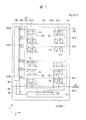
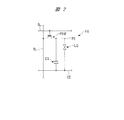
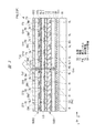
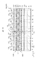
図1は、実施の形態1の表示装置の一例を示す平面図である。図2は、実施の形態1の表示装置における画素を示す等価回路図である。図3は、実施の形態1の表示装置の一例を示す断面図である。図4は、実施の形態1の表示装置における共通電極の配置の一例を示す平面図である。なお、図3では、実際には図3の断面には配置されていない走査線GLを便宜上一緒に示している。
次に、表示装置DSPが、検出電極Rxを利用して指などの物体からなる入力具の位置、すなわち入力位置を検出する方法について説明する。
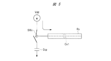
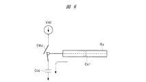
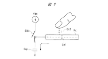
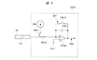
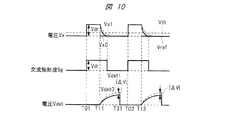
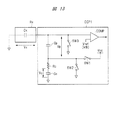
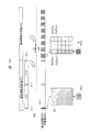
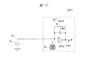
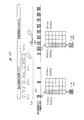
次に、本実施の形態1の表示装置におけるタッチ検出方法およびタッチ検出回路について説明する。
次に、比較例のタッチ検出方法およびタッチ検出回路について説明し、比較例のタッチ検出方法およびタッチ検出回路における問題点について説明する。
本実施の形態1の表示装置における技術的思想は、このような比較例の表示装置の問題点を解決するためのものであり、検出モードとしての指座標検出処理の前に待機モードとして行われる指近接検出処理において、検出処理に要する時間を短くし、消費電力を低減しつつ、検出ミスの発生を防止または抑制するためのものである。
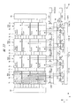
次に、実施の形態1の第1変形例について説明する。図24は、実施の形態1の表示装置の第1変形例におけるタッチ検出回路を示す図である。なお、図24は、複数のシールド電極SHにハッチングを付すことにより、ステップS11において、複数のシールド電極SHの各々が選択されている状態を示している。
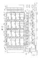
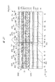
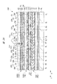
次に、実施の形態1の第2変形例について説明する。図25は、実施の形態1の表示装置の第2変形例の一例を示す断面図である。図26は、実施の形態1の表示装置の第2変形例の別の例におけるタッチ検出回路を示す図である。
次に、実施の形態1の第3変形例について説明する。図27は、実施の形態1の表示装置の第3変形例の一例を示す断面図である。
次に、実施の形態1の第4変形例について説明する。図28は、実施の形態1の表示装置の第4変形例の一例を示す断面図である。
実施の形態1では、入力装置としてのタッチパネルを、入力装置の検出電極が、表示装置の表示パネル内に設けられ、かつ、表示装置の共通電極として機能するインセル型のタッチ検出機能付き表示装置に適用した例について説明した。それに対して、実施の形態2では、入力装置としてのタッチパネルを、液晶表示装置の表示面側に外付けすることによって、入力装置の検出電極が、表示装置の表示パネル内に設けられず、表示装置の共通電極としても機能しないオンセル型のタッチ検出機能付き表示装置に適用した例について説明する。なお、本実施の形態2の表示装置に備えられた入力装置は、液晶表示装置を始めとして、有機EL(Electroluminescence)表示装置などの各種の表示装置の表示面側に外付けすることが可能である。
図29は、実施の形態2の表示装置を示す断面図である。図29に示すように、表示装置DSPは、入力装置TCPを有する。入力装置TCPは、表示パネルPNLに対して第1の側(図29中上側)に配置されている。言い換えれば、入力装置TCPは、表示パネルPNLの前面FSと対向配置されている。なお、表示装置DSPは、入力装置TCPに対して表示パネルPNL側と反対側に配置されたカバー板40を有してもよい。カバー板40として、ガラス基板や樹脂基板などの光透過性を有する絶縁基板を用いることができる。また、タッチ検出面TDSは、カバー板40の面であって、基板SUB2側と反対側の面である。
11〜13 絶縁膜
20、30 絶縁基板
40 カバー板
31 絶縁膜
AL1、AL2 配向膜
AR1、AR2 領域
BL バックライトユニット
BM ブラックマトリクス
BS、BS1 背面
Cc、Ccf、Ccp、Ccs、Cdet、Cp、Cx、Cx1、Cx2 容量
CE 共通電極
CFB、CFG、CFR カラーフィルタ
CLC1 クロック信号供給回路
CNC1、CNC2 接続回路
COMP 比較器
CS 保持容量
CSW スイッチング素子
DA 表示領域
DCP1、DCP2 検出回路
DET 電圧検出器
DS 表示面
DSP 表示装置
DSW スイッチング素子
FS、FS1 前面
G1 信号
GD 走査線駆動回路
GL、GL1、GL2、GL3、GLn 走査線
GSC1 ガード信号供給回路
GSP 切り替え部
GSW スイッチング素子
IC1 駆動ICチップ
LQ 液晶層
MU1 マルチプレクサ回路
NDA 非表示領域
OCL オーバーコート層
OD1、OD2 光学素子
OPdet オペアンプ
PE 画素電極
PNL 表示パネル
PSW 画素スイッチング素子
PX 画素
Rc 抵抗
Reset 期間
RG、RG1〜RG4 電極群
Rx 検出電極
Rx1、Rx11〜Rx14、Rx2、Rx21〜Rx24 検出電極
Rx3、Rx31〜Rx34、Rx4、Rx41〜Rx44 検出電極
Rxn−1、Rxn、Rxn+1 検出電極
Rxs 選択検出電極
Rxu 非選択検出電極
SD 信号線駆動回路
SE 検出部
Sg 交流矩形波
SH シールド電極
SL、SL1、SL2、SLm 信号線
SLT スリット
SP 空間
SSP1、SSP2 切り替え部
SSW1、SSW2 スイッチング素子
SUB1〜SUB3 基板
SW1〜SW3、SWc1〜SWc3 スイッチ
SWc 制御スイッチ
T01、T02、T11、T12、T31 時刻
TCP 入力装置
Td トランジスタ
Td1、Td11〜Td14、Td2、Td21〜Td24 トランジスタ
Td3、Td31〜Td34、Td4、Td41〜Td44 トランジスタ
Tg トランジスタ
TDS タッチ検出面
TG、TG1〜TG4 トランジスタ群
V1、V11、V12、V2 電圧
Vc、Vcc、Vdet、Vdr、Vp、Vx 電圧
Vdd 電源
Vdet0、Vdet1、Vx0、Vx1 波形
Vref 参照信号
VSC1、VSC2 電圧供給回路
Vth 閾値電圧
W1、W2 配線
Claims (17)
- 第1の側の第1面、および、前記第1の側と反対側の第2面を有し、前記第1面に画像が表示される表示パネルと、
平面視において前記表示パネルと重なる複数の第1電極と、
平面視において前記表示パネルと重なる第2電極と、
を有し、
前記第2電極は、前記複数の第1電極に対して前記第1の側と反対側に配置され、
前記第2電極の静電容量に基づいて、前記第1面への物体の近接または接触が検出され、
前記複数の第1電極の各々の静電容量に基づいて、前記第1面に近接または接触した前記物体の位置が検出される、表示装置。 - 請求項1記載の表示装置において、
平面視において、第1方向にそれぞれ延在し、かつ、前記第1方向と交差する第2方向に配列された複数の前記第2電極を有し、
前記複数の第2電極の各々の静電容量に基づいて、前記物体の近接または接触が検出される、表示装置。 - 請求項2記載の表示装置において、
前記複数の第2電極の各々は、走査線または信号線である、表示装置。 - 請求項1記載の表示装置において、
前記複数の第1電極は、前記表示パネル内に配置されている、表示装置。 - 請求項4記載の表示装置において、
前記表示パネルは、
第1基板と、
前記第1基板に対して前記第1の側に配置された第2基板と、
を含み、
前記第2電極は、前記第1基板に対して前記第1の側と反対側に配置されている、表示装置。 - 請求項5記載の表示装置において、
前記第1基板と前記第2電極との間に空間が設けられている、表示装置。 - 請求項5記載の表示装置において、
前記表示パネルは、前記第1基板と前記第2基板との間に配置された液晶層を含み、
前記複数の第1電極は、前記第1基板と前記液晶層との間に配置されている、表示装置。 - 請求項1記載の表示装置において、
前記第2電極は、平面視において前記複数の第1電極の各々と重なり、
前記複数の第1電極の各々が電気的に浮遊した状態で、前記第2電極の静電容量に基づいて、前記物体の近接または接触が検出される、表示装置。 - 請求項8記載の表示装置において、
平面視において第3方向にそれぞれ延在し、かつ、前記第3方向と交差する第4方向に配列された複数の走査線と、
平面視において前記第4方向にそれぞれ延在し、かつ、前記第3方向に配列された複数の信号線と、
を有し、
前記第2電極は、平面視において前記複数の走査線および前記複数の信号線の各々と重なり、
前記複数の走査線および前記複数の信号線の各々が電気的に浮遊した状態で、前記第2電極の静電容量に基づいて、前記物体の近接または接触が検出される、表示装置。 - 請求項1記載の表示装置において、
前記表示パネルに対して前記第1の側に配置された第3基板を有し、
前記複数の第1電極は、前記第3基板に対して前記第1の側に配置され、
前記第2電極は、前記第3基板と前記表示パネルとの間に配置されている、表示装置。 - 請求項1記載の表示装置において、
前記複数の第1電極および前記第2電極の各々の静電容量を検出する検出部を有し、
前記検出部は、前記第2電極の静電容量を検出することにより、前記物体の近接または接触を検出する第1検出処理を行い、
前記第1検出処理において、前記物体の近接または接触が検出されなかったとき、前記検出部は、前記第1検出処理を繰り返し、
前記第1検出処理において、前記物体の近接または接触が検出されたとき、前記検出部は、前記複数の第1電極の各々の静電容量を個別に検出することにより、前記物体の位置を検出する第2検出処理を行う、表示装置。 - 請求項11記載の表示装置において、
前記検出部は、
前記複数の第1電極の各々の静電容量を検出する第1検出回路と、
前記第2電極の静電容量を検出する第2検出回路と、
前記第1検出回路と前記複数の第1電極との接続状態を切り替える切り替え部と、
を含み、
前記検出部は、前記第1検出処理において、前記第2電極の静電容量を前記第2検出回路により検出し、
前記検出部は、前記第2検出処理において、前記切り替え部により前記複数の第1電極を前記第1検出回路に接続することにより、前記複数の第1電極の各々の静電容量を個別に検出し、
前記検出部は、前記切り替え部により前記複数の第1電極の各々を電気的に浮遊させた状態で、前記第1検出処理を行う、表示装置。 - 第1の側の第1面、および、前記第1の側と反対側の第2面を有する基板と、
平面視において前記基板と重なる複数の第1電極と、
平面視において前記基板と重なる第2電極と、
を有し、
前記第2電極は、前記複数の第1電極に対して前記第1の側と反対側に配置され、
前記第2電極の静電容量に基づいて、前記第1面への物体の近接または接触が検出され、
前記複数の第1電極の各々の静電容量に基づいて、前記第1面に近接または接触した前記物体の位置が検出される、入力装置。 - 請求項13記載の入力装置において、
平面視において第1方向にそれぞれ延在し、かつ、前記第1方向と交差する第2方向に配列された複数の前記第2電極を有し、
前記複数の第2電極の各々の静電容量に基づいて、前記物体の近接または接触が検出される、入力装置。 - 請求項13記載の入力装置において、
前記第2電極は、平面視において前記複数の第1電極の各々と重なり、
前記複数の第1電極の各々が電気的に浮遊した状態で、前記第2電極の静電容量に基づいて、前記物体の近接または接触が検出される、入力装置。 - 請求項13記載の入力装置において、
前記複数の第1電極および前記第2電極の各々の静電容量を検出する検出部を有し、
前記検出部は、前記第2電極の静電容量を検出することにより、前記物体の近接または接触を検出する第1検出処理を行い、
前記第1検出処理において、前記物体の近接または接触が検出されなかったとき、前記検出部は、前記第1検出処理を繰り返し、
前記第1検出処理において、前記物体の近接または接触が検出されたとき、前記検出部は、前記複数の第1電極の各々の静電容量を個別に検出することにより、前記物体の位置を検出する第2検出処理を行う、入力装置。 - 請求項16記載の入力装置において、
前記検出部は、
前記複数の第1電極の各々の静電容量を検出する第1検出回路と、
前記第2電極の静電容量を検出する第2検出回路と、
前記第1検出回路と前記複数の第1電極との接続状態を切り替える切り替え部と、
を含み、
前記検出部は、前記第1検出処理において、前記第2電極の静電容量を前記第2検出回路により検出し、
前記検出部は、前記第2検出処理において、前記切り替え部により前記複数の第1電極を前記第1検出回路に接続することにより、前記複数の第1電極の各々の静電容量を個別に検出し、
前記検出部は、前記切り替え部により前記複数の第1電極の各々を電気的に浮遊させた状態で、前記第1検出処理を行う、入力装置。
Priority Applications (3)
| Application Number | Priority Date | Filing Date | Title |
|---|---|---|---|
| JP2015237258A JP6698324B2 (ja) | 2015-12-04 | 2015-12-04 | 表示装置および入力装置 |
| US15/354,410 US10216320B2 (en) | 2015-12-04 | 2016-11-17 | Display device and input device |
| US16/244,558 US10365759B2 (en) | 2015-12-04 | 2019-01-10 | Display device and input device |
Applications Claiming Priority (1)
| Application Number | Priority Date | Filing Date | Title |
|---|---|---|---|
| JP2015237258A JP6698324B2 (ja) | 2015-12-04 | 2015-12-04 | 表示装置および入力装置 |
Publications (3)
| Publication Number | Publication Date |
|---|---|
| JP2017102811A true JP2017102811A (ja) | 2017-06-08 |
| JP2017102811A5 JP2017102811A5 (ja) | 2018-09-27 |
| JP6698324B2 JP6698324B2 (ja) | 2020-05-27 |
Family
ID=58798256
Family Applications (1)
| Application Number | Title | Priority Date | Filing Date |
|---|---|---|---|
| JP2015237258A Active JP6698324B2 (ja) | 2015-12-04 | 2015-12-04 | 表示装置および入力装置 |
Country Status (2)
| Country | Link |
|---|---|
| US (2) | US10216320B2 (ja) |
| JP (1) | JP6698324B2 (ja) |
Cited By (3)
| Publication number | Priority date | Publication date | Assignee | Title |
|---|---|---|---|---|
| JP2019125218A (ja) * | 2018-01-18 | 2019-07-25 | 三菱電機株式会社 | タッチパネル及び表示装置 |
| WO2019187405A1 (ja) | 2018-03-26 | 2019-10-03 | アルプスアルパイン株式会社 | 検出装置および制御装置 |
| JPWO2023188080A1 (ja) * | 2022-03-30 | 2023-10-05 |
Families Citing this family (11)
| Publication number | Priority date | Publication date | Assignee | Title |
|---|---|---|---|---|
| TWI566120B (zh) * | 2015-05-21 | 2017-01-11 | 速博思股份有限公司 | 具有反射遮蔽電極之生物辨識裝置及其偵測控制方法 |
| JP6698324B2 (ja) * | 2015-12-04 | 2020-05-27 | 株式会社ジャパンディスプレイ | 表示装置および入力装置 |
| JP2019041968A (ja) * | 2017-08-31 | 2019-03-22 | パナソニックIpマネジメント株式会社 | 炊飯器 |
| CN108169944A (zh) * | 2017-11-30 | 2018-06-15 | 维沃移动通信有限公司 | 一种液晶显示模块及其制作方法、移动终端 |
| KR102522290B1 (ko) * | 2018-04-05 | 2023-04-19 | 삼성디스플레이 주식회사 | 표시 장치 |
| CN109656430A (zh) * | 2019-01-16 | 2019-04-19 | 汕头超声显示器技术有限公司 | 一种具有接近探测功能的电容触摸屏 |
| KR102826480B1 (ko) | 2019-08-23 | 2025-06-30 | 엘지전자 주식회사 | 인공 지능을 통해 구속 상황을 회피하는 로봇 청소기 및 그의 동작 방법 |
| JP7383869B2 (ja) * | 2020-02-13 | 2023-11-21 | シャープ株式会社 | タッチパネル及び表示装置 |
| JP2022018722A (ja) * | 2020-07-16 | 2022-01-27 | シャープ株式会社 | タッチパネル装置 |
| DE102021128566A1 (de) * | 2020-11-30 | 2022-06-02 | Lg Display Co., Ltd. | Berührungsanzeigevorrichtung, Ansteuerschaltung und Ansteuerverfahren dafür |
| EP4040680A1 (en) * | 2021-02-08 | 2022-08-10 | Alps Alpine Co., Ltd. | Electrostatic-capacitive proximity detecting device and method for detecting position of to-be-detected object |
Citations (5)
| Publication number | Priority date | Publication date | Assignee | Title |
|---|---|---|---|---|
| JP2010015505A (ja) * | 2008-07-07 | 2010-01-21 | Toshiba Mobile Display Co Ltd | 表示装置 |
| JP2012512457A (ja) * | 2008-12-15 | 2012-05-31 | ソニー エリクソン モバイル コミュニケーションズ, エービー | 静電容量に基づく近接検出を行うセンサプレートの層及び関連するタッチパネルを備えたタッチ感応ディスプレイ |
| JP2012512456A (ja) * | 2008-12-15 | 2012-05-31 | ソニー エリクソン モバイル コミュニケーションズ, エービー | 同一平面の静電容量式タッチセンサパッド及び近接センサパッドと、関連するタッチパネルとを備えたタッチ感応ディスプレイ |
| JP2015018424A (ja) * | 2013-07-11 | 2015-01-29 | 三菱電機株式会社 | タッチパネル、タッチパネル付き表示装置 |
| JP2015049848A (ja) * | 2013-09-04 | 2015-03-16 | アルプス電気株式会社 | 入力装置及びその検出方法 |
Family Cites Families (9)
| Publication number | Priority date | Publication date | Assignee | Title |
|---|---|---|---|---|
| JP5164930B2 (ja) * | 2009-06-05 | 2013-03-21 | 株式会社ジャパンディスプレイウェスト | タッチパネル、表示パネル、および表示装置 |
| JP5653686B2 (ja) * | 2010-08-24 | 2015-01-14 | 株式会社ジャパンディスプレイ | タッチ検出機能付き表示装置 |
| JP2014191660A (ja) * | 2013-03-27 | 2014-10-06 | Japan Display Inc | タッチ検出機能付き表示装置及び電子機器 |
| JP5807035B2 (ja) * | 2013-03-29 | 2015-11-10 | 株式会社ジャパンディスプレイ | タッチ検出機能付き表示装置、電子機器及びタッチ検出デバイス |
| JP6184317B2 (ja) | 2013-12-24 | 2017-08-23 | アルプス電気株式会社 | 入力装置 |
| JP2015143933A (ja) * | 2014-01-31 | 2015-08-06 | 株式会社ジャパンディスプレイ | 静電容量型センサ付き表示装置及びその駆動方法 |
| US20150309636A1 (en) * | 2014-04-25 | 2015-10-29 | Japan Display Inc. | Sensor-equipped display device |
| JP6205312B2 (ja) * | 2014-06-18 | 2017-09-27 | 株式会社ジャパンディスプレイ | 液晶表示装置 |
| JP6698324B2 (ja) * | 2015-12-04 | 2020-05-27 | 株式会社ジャパンディスプレイ | 表示装置および入力装置 |
-
2015
- 2015-12-04 JP JP2015237258A patent/JP6698324B2/ja active Active
-
2016
- 2016-11-17 US US15/354,410 patent/US10216320B2/en active Active
-
2019
- 2019-01-10 US US16/244,558 patent/US10365759B2/en active Active
Patent Citations (5)
| Publication number | Priority date | Publication date | Assignee | Title |
|---|---|---|---|---|
| JP2010015505A (ja) * | 2008-07-07 | 2010-01-21 | Toshiba Mobile Display Co Ltd | 表示装置 |
| JP2012512457A (ja) * | 2008-12-15 | 2012-05-31 | ソニー エリクソン モバイル コミュニケーションズ, エービー | 静電容量に基づく近接検出を行うセンサプレートの層及び関連するタッチパネルを備えたタッチ感応ディスプレイ |
| JP2012512456A (ja) * | 2008-12-15 | 2012-05-31 | ソニー エリクソン モバイル コミュニケーションズ, エービー | 同一平面の静電容量式タッチセンサパッド及び近接センサパッドと、関連するタッチパネルとを備えたタッチ感応ディスプレイ |
| JP2015018424A (ja) * | 2013-07-11 | 2015-01-29 | 三菱電機株式会社 | タッチパネル、タッチパネル付き表示装置 |
| JP2015049848A (ja) * | 2013-09-04 | 2015-03-16 | アルプス電気株式会社 | 入力装置及びその検出方法 |
Cited By (5)
| Publication number | Priority date | Publication date | Assignee | Title |
|---|---|---|---|---|
| JP2019125218A (ja) * | 2018-01-18 | 2019-07-25 | 三菱電機株式会社 | タッチパネル及び表示装置 |
| WO2019187405A1 (ja) | 2018-03-26 | 2019-10-03 | アルプスアルパイン株式会社 | 検出装置および制御装置 |
| JPWO2023188080A1 (ja) * | 2022-03-30 | 2023-10-05 | ||
| WO2023188080A1 (ja) * | 2022-03-30 | 2023-10-05 | シャープディスプレイテクノロジー株式会社 | タッチセンサ、表示装置 |
| JP7723833B2 (ja) | 2022-03-30 | 2025-08-14 | シャープディスプレイテクノロジー株式会社 | タッチセンサ、表示装置 |
Also Published As
| Publication number | Publication date |
|---|---|
| US10216320B2 (en) | 2019-02-26 |
| JP6698324B2 (ja) | 2020-05-27 |
| US20170160863A1 (en) | 2017-06-08 |
| US10365759B2 (en) | 2019-07-30 |
| US20190163317A1 (en) | 2019-05-30 |
Similar Documents
| Publication | Publication Date | Title |
|---|---|---|
| JP6698324B2 (ja) | 表示装置および入力装置 | |
| US12044941B2 (en) | Display device | |
| CN107272239B (zh) | 显示装置 | |
| JP6560971B2 (ja) | 表示装置および入力装置 | |
| CN112860134B (zh) | 带传感器的显示装置及其驱动方法 | |
| US10754473B2 (en) | Display device and driving method | |
| CN105467699B (zh) | 带有传感器的显示装置以及显示装置的控制方法 | |
| JP6620058B2 (ja) | 表示装置 |
Legal Events
| Date | Code | Title | Description |
|---|---|---|---|
| A521 | Request for written amendment filed |
Free format text: JAPANESE INTERMEDIATE CODE: A523 Effective date: 20180810 |
|
| A621 | Written request for application examination |
Free format text: JAPANESE INTERMEDIATE CODE: A621 Effective date: 20180810 |
|
| A977 | Report on retrieval |
Free format text: JAPANESE INTERMEDIATE CODE: A971007 Effective date: 20190218 |
|
| A131 | Notification of reasons for refusal |
Free format text: JAPANESE INTERMEDIATE CODE: A131 Effective date: 20190402 |
|
| A521 | Request for written amendment filed |
Free format text: JAPANESE INTERMEDIATE CODE: A523 Effective date: 20190524 |
|
| A02 | Decision of refusal |
Free format text: JAPANESE INTERMEDIATE CODE: A02 Effective date: 20191105 |
|
| A521 | Request for written amendment filed |
Free format text: JAPANESE INTERMEDIATE CODE: A523 Effective date: 20200130 |
|
| A911 | Transfer to examiner for re-examination before appeal (zenchi) |
Free format text: JAPANESE INTERMEDIATE CODE: A911 Effective date: 20200206 |
|
| TRDD | Decision of grant or rejection written | ||
| A01 | Written decision to grant a patent or to grant a registration (utility model) |
Free format text: JAPANESE INTERMEDIATE CODE: A01 Effective date: 20200407 |
|
| A61 | First payment of annual fees (during grant procedure) |
Free format text: JAPANESE INTERMEDIATE CODE: A61 Effective date: 20200428 |
|
| R150 | Certificate of patent or registration of utility model |
Ref document number: 6698324 Country of ref document: JP Free format text: JAPANESE INTERMEDIATE CODE: R150 |
|
| R250 | Receipt of annual fees |
Free format text: JAPANESE INTERMEDIATE CODE: R250 |
|
| R250 | Receipt of annual fees |
Free format text: JAPANESE INTERMEDIATE CODE: R250 |
|
| R250 | Receipt of annual fees |
Free format text: JAPANESE INTERMEDIATE CODE: R250 |
|
| S111 | Request for change of ownership or part of ownership |
Free format text: JAPANESE INTERMEDIATE CODE: R313113 |
|
| R350 | Written notification of registration of transfer |
Free format text: JAPANESE INTERMEDIATE CODE: R350 |