JP2017103403A - ドライエッチング方法 - Google Patents
ドライエッチング方法 Download PDFInfo
- Publication number
- JP2017103403A JP2017103403A JP2015237091A JP2015237091A JP2017103403A JP 2017103403 A JP2017103403 A JP 2017103403A JP 2015237091 A JP2015237091 A JP 2015237091A JP 2015237091 A JP2015237091 A JP 2015237091A JP 2017103403 A JP2017103403 A JP 2017103403A
- Authority
- JP
- Japan
- Prior art keywords
- etching
- dry etching
- shape
- etching method
- gas
- Prior art date
- Legal status (The legal status is an assumption and is not a legal conclusion. Google has not performed a legal analysis and makes no representation as to the accuracy of the status listed.)
- Granted
Links
Images


Classifications
-
- H—ELECTRICITY
- H10—SEMICONDUCTOR DEVICES; ELECTRIC SOLID-STATE DEVICES NOT OTHERWISE PROVIDED FOR
- H10P—GENERIC PROCESSES OR APPARATUS FOR THE MANUFACTURE OR TREATMENT OF DEVICES COVERED BY CLASS H10
- H10P50/00—Etching of wafers, substrates or parts of devices
- H10P50/20—Dry etching; Plasma etching; Reactive-ion etching
- H10P50/24—Dry etching; Plasma etching; Reactive-ion etching of semiconductor materials
- H10P50/242—Dry etching; Plasma etching; Reactive-ion etching of semiconductor materials of Group IV materials
-
- H—ELECTRICITY
- H10—SEMICONDUCTOR DEVICES; ELECTRIC SOLID-STATE DEVICES NOT OTHERWISE PROVIDED FOR
- H10D—INORGANIC ELECTRIC SEMICONDUCTOR DEVICES
- H10D30/00—Field-effect transistors [FET]
- H10D30/01—Manufacture or treatment
- H10D30/021—Manufacture or treatment of FETs having insulated gates [IGFET]
- H10D30/024—Manufacture or treatment of FETs having insulated gates [IGFET] of fin field-effect transistors [FinFET]
-
- H—ELECTRICITY
- H10—SEMICONDUCTOR DEVICES; ELECTRIC SOLID-STATE DEVICES NOT OTHERWISE PROVIDED FOR
- H10D—INORGANIC ELECTRIC SEMICONDUCTOR DEVICES
- H10D30/00—Field-effect transistors [FET]
- H10D30/60—Insulated-gate field-effect transistors [IGFET]
- H10D30/62—Fin field-effect transistors [FinFET]
-
- H—ELECTRICITY
- H10—SEMICONDUCTOR DEVICES; ELECTRIC SOLID-STATE DEVICES NOT OTHERWISE PROVIDED FOR
- H10P—GENERIC PROCESSES OR APPARATUS FOR THE MANUFACTURE OR TREATMENT OF DEVICES COVERED BY CLASS H10
- H10P14/00—Formation of materials, e.g. in the shape of layers or pillars
- H10P14/60—Formation of materials, e.g. in the shape of layers or pillars of insulating materials
- H10P14/65—Formation of materials, e.g. in the shape of layers or pillars of insulating materials characterised by treatments performed before or after the formation of the materials
- H10P14/6502—Formation of materials, e.g. in the shape of layers or pillars of insulating materials characterised by treatments performed before or after the formation of the materials of treatments performed before formation of the materials
- H10P14/6512—Formation of materials, e.g. in the shape of layers or pillars of insulating materials characterised by treatments performed before or after the formation of the materials of treatments performed before formation of the materials by exposure to a gas or vapour
- H10P14/6514—Formation of materials, e.g. in the shape of layers or pillars of insulating materials characterised by treatments performed before or after the formation of the materials of treatments performed before formation of the materials by exposure to a gas or vapour by exposure to a plasma
-
- H—ELECTRICITY
- H10—SEMICONDUCTOR DEVICES; ELECTRIC SOLID-STATE DEVICES NOT OTHERWISE PROVIDED FOR
- H10P—GENERIC PROCESSES OR APPARATUS FOR THE MANUFACTURE OR TREATMENT OF DEVICES COVERED BY CLASS H10
- H10P50/00—Etching of wafers, substrates or parts of devices
- H10P50/20—Dry etching; Plasma etching; Reactive-ion etching
- H10P50/26—Dry etching; Plasma etching; Reactive-ion etching of conductive or resistive materials
- H10P50/262—Dry etching; Plasma etching; Reactive-ion etching of conductive or resistive materials by physical means only
- H10P50/263—Dry etching; Plasma etching; Reactive-ion etching of conductive or resistive materials by physical means only of silicon-containing layers
-
- H—ELECTRICITY
- H10—SEMICONDUCTOR DEVICES; ELECTRIC SOLID-STATE DEVICES NOT OTHERWISE PROVIDED FOR
- H10P—GENERIC PROCESSES OR APPARATUS FOR THE MANUFACTURE OR TREATMENT OF DEVICES COVERED BY CLASS H10
- H10P50/00—Etching of wafers, substrates or parts of devices
- H10P50/20—Dry etching; Plasma etching; Reactive-ion etching
- H10P50/26—Dry etching; Plasma etching; Reactive-ion etching of conductive or resistive materials
- H10P50/264—Dry etching; Plasma etching; Reactive-ion etching of conductive or resistive materials by chemical means
- H10P50/266—Dry etching; Plasma etching; Reactive-ion etching of conductive or resistive materials by chemical means by vapour etching only
- H10P50/267—Dry etching; Plasma etching; Reactive-ion etching of conductive or resistive materials by chemical means by vapour etching only using plasmas
- H10P50/268—Dry etching; Plasma etching; Reactive-ion etching of conductive or resistive materials by chemical means by vapour etching only using plasmas of silicon-containing layers
-
- H—ELECTRICITY
- H10—SEMICONDUCTOR DEVICES; ELECTRIC SOLID-STATE DEVICES NOT OTHERWISE PROVIDED FOR
- H10P—GENERIC PROCESSES OR APPARATUS FOR THE MANUFACTURE OR TREATMENT OF DEVICES COVERED BY CLASS H10
- H10P50/00—Etching of wafers, substrates or parts of devices
- H10P50/20—Dry etching; Plasma etching; Reactive-ion etching
- H10P50/28—Dry etching; Plasma etching; Reactive-ion etching of insulating materials
- H10P50/282—Dry etching; Plasma etching; Reactive-ion etching of insulating materials of inorganic materials
- H10P50/283—Dry etching; Plasma etching; Reactive-ion etching of insulating materials of inorganic materials by chemical means
-
- H—ELECTRICITY
- H10—SEMICONDUCTOR DEVICES; ELECTRIC SOLID-STATE DEVICES NOT OTHERWISE PROVIDED FOR
- H10P—GENERIC PROCESSES OR APPARATUS FOR THE MANUFACTURE OR TREATMENT OF DEVICES COVERED BY CLASS H10
- H10P50/00—Etching of wafers, substrates or parts of devices
- H10P50/69—Etching of wafers, substrates or parts of devices using masks for semiconductor materials
- H10P50/691—Etching of wafers, substrates or parts of devices using masks for semiconductor materials for Group V materials or Group III-V materials
Landscapes
- Drying Of Semiconductors (AREA)
- Physics & Mathematics (AREA)
- Engineering & Computer Science (AREA)
- Plasma & Fusion (AREA)
- Chemical & Material Sciences (AREA)
- Inorganic Chemistry (AREA)
Abstract
Description
T=(W/2)/S (1)
T=エッチング時間(秒)
W=パターン間のスペース幅(nm)
S=エッチング速度(nm/秒)
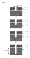
(1)式より本実施例では、パターン間のスペース幅が40nm、エッチング速度が1.0nm/秒であったことから、反応性イオンアシストエッチステップの処理時間を20秒と設定した。よって、より裾引き形状を効率よく除去するためには、(1)式で求められる処理時間以下の時間によりイオンアシストエッチステップを挿入する必要がある。言い換えると、反応性イオンアシストエッチステップの処理時間は、(1)式で求められる時間以下の時間とすれば良い。
102 SiO2膜
103 SiN膜
Claims (8)
- マスク選択比を維持しながら垂直形状にプラズマエッチングするドライエッチング方法において、
反応性ガスを用いて被エッチング膜をエッチングすることにより前記被エッチング膜のエッチング形状が裾引き形状となる第一の工程と、
前記第一の工程後、スパッタエッチングにより前記裾引き形状を垂直形状にする第二の工程とを有することを特徴とするドライエッチング方法。 - マスク選択比を維持しながら垂直形状にプラズマエッチングするドライエッチング方法において、
反応性ガスを用いて被エッチング膜をエッチングすることにより前記被エッチング膜のエッチング形状が裾引き形状となる第一の工程と、
前記第一の工程後、不活性ガスのみを用いて前記第一工程後の被エッチング膜をスパッタエッチングする第二の工程とを有することを特徴とするドライエッチング方法。 - 請求項1または請求項2に記載のドライエッチング方法において、
前記第一の工程と前記第二の工程を繰り返すことを特徴とするドライエッチング方法。 - 請求項1または請求項2に記載のドライエッチング方法において、
前記被エッチング膜は、シリコン元素を含有する材料であることを特徴とするドライエッチング方法。 - 請求項1または請求項2に記載のドライエッチング方法において、
前記被エッチング膜の構造は、高アスペクト比の構造であることを特徴とするドライエッチング方法。 - 請求項1ないし請求項5のいずれか一項に記載のドライエッチング方法において、
前記第二の工程の前記被エッチング膜に印加する高周波バイアス電力を前記第一の工程の前記被エッチング膜に印加する高周波バイアス電力より高くすることを特徴とするドライエッチング方法。 - 請求項1ないし請求項6のいずれか一項に記載のドライエッチング方法において、
前記第一の工程の時間は、前記マスクのパターン間のスペース幅における半分の値を前記第一の工程のエッチング速度により除した値以下の時間であることを特徴とするドライエッチング方法。 - 請求項2に記載のドライエッチング方法において、
前記不活性ガスは、Heガス、Neガス、Arガス、Krガス、Xeガス、N2ガスの中の少なくともいずれか一つのガスであることを特徴とするドライエッチング方法。
Priority Applications (4)
| Application Number | Priority Date | Filing Date | Title |
|---|---|---|---|
| JP2015237091A JP6557588B2 (ja) | 2015-12-04 | 2015-12-04 | ドライエッチング方法 |
| KR1020160098401A KR101870221B1 (ko) | 2015-12-04 | 2016-08-02 | 드라이 에칭 방법 |
| TW105126381A TWI630655B (zh) | 2015-12-04 | 2016-08-18 | Dry etching method |
| US15/248,171 US10192749B2 (en) | 2015-12-04 | 2016-08-26 | Dry-etching method |
Applications Claiming Priority (1)
| Application Number | Priority Date | Filing Date | Title |
|---|---|---|---|
| JP2015237091A JP6557588B2 (ja) | 2015-12-04 | 2015-12-04 | ドライエッチング方法 |
Publications (3)
| Publication Number | Publication Date |
|---|---|
| JP2017103403A true JP2017103403A (ja) | 2017-06-08 |
| JP2017103403A5 JP2017103403A5 (ja) | 2018-02-01 |
| JP6557588B2 JP6557588B2 (ja) | 2019-08-07 |
Family
ID=58800394
Family Applications (1)
| Application Number | Title | Priority Date | Filing Date |
|---|---|---|---|
| JP2015237091A Active JP6557588B2 (ja) | 2015-12-04 | 2015-12-04 | ドライエッチング方法 |
Country Status (4)
| Country | Link |
|---|---|
| US (1) | US10192749B2 (ja) |
| JP (1) | JP6557588B2 (ja) |
| KR (1) | KR101870221B1 (ja) |
| TW (1) | TWI630655B (ja) |
Cited By (1)
| Publication number | Priority date | Publication date | Assignee | Title |
|---|---|---|---|---|
| WO2024117212A1 (ja) * | 2022-12-01 | 2024-06-06 | 東京エレクトロン株式会社 | エッチング方法及びプラズマ処理装置 |
Citations (5)
| Publication number | Priority date | Publication date | Assignee | Title |
|---|---|---|---|---|
| JP2005347585A (ja) * | 2004-06-04 | 2005-12-15 | Hitachi Ltd | 半導体デバイス製造方法およびそのシステム |
| JP2011238935A (ja) * | 2004-07-02 | 2011-11-24 | Ulvac Japan Ltd | エッチング方法及び装置 |
| JP2015023157A (ja) * | 2013-07-19 | 2015-02-02 | キヤノン株式会社 | シリコン基板のエッチング方法 |
| US20150056817A1 (en) * | 2013-08-26 | 2015-02-26 | Tokyo Electron Limited | Semiconductor device manufacturing method |
| JP2017092376A (ja) * | 2015-11-16 | 2017-05-25 | 東京エレクトロン株式会社 | エッチング方法 |
Family Cites Families (13)
| Publication number | Priority date | Publication date | Assignee | Title |
|---|---|---|---|---|
| JPH0665214B2 (ja) | 1985-05-17 | 1994-08-22 | 日本電信電話株式会社 | 半導体装置の製造方法 |
| JP3094470B2 (ja) * | 1991-01-22 | 2000-10-03 | ソニー株式会社 | ドライエッチング方法 |
| JPH04354331A (ja) * | 1991-05-31 | 1992-12-08 | Sony Corp | ドライエッチング方法 |
| DE4219765A1 (de) | 1992-06-17 | 1993-12-23 | Bayer Ag | Substituierte (Benzothiazolyl- und Chinoxalyl-methoxy)phenylessigsäurederivate |
| US6191043B1 (en) * | 1999-04-20 | 2001-02-20 | Lam Research Corporation | Mechanism for etching a silicon layer in a plasma processing chamber to form deep openings |
| US6540885B1 (en) * | 2001-01-30 | 2003-04-01 | Lam Research Corp. | Profile control of oxide trench features for dual damascene applications |
| JP4128365B2 (ja) * | 2002-02-07 | 2008-07-30 | 東京エレクトロン株式会社 | エッチング方法及びエッチング装置 |
| US20050029221A1 (en) * | 2003-08-09 | 2005-02-10 | Taiwan Semiconductor Manufacturing Co., Ltd. | Deep trench etching using HDP chamber |
| US7405162B2 (en) * | 2004-09-22 | 2008-07-29 | Tokyo Electron Limited | Etching method and computer-readable storage medium |
| JP4450245B2 (ja) * | 2007-06-07 | 2010-04-14 | 株式会社デンソー | 半導体装置の製造方法 |
| US8598040B2 (en) * | 2011-09-06 | 2013-12-03 | Lam Research Corporation | ETCH process for 3D flash structures |
| JP5932599B2 (ja) * | 2011-10-31 | 2016-06-08 | 株式会社日立ハイテクノロジーズ | プラズマエッチング方法 |
| US9224615B2 (en) * | 2013-09-11 | 2015-12-29 | Taiwan Semiconductor Manufacturing Co., Ltd. | Noble gas bombardment to reduce scallops in bosch etching |
-
2015
- 2015-12-04 JP JP2015237091A patent/JP6557588B2/ja active Active
-
2016
- 2016-08-02 KR KR1020160098401A patent/KR101870221B1/ko active Active
- 2016-08-18 TW TW105126381A patent/TWI630655B/zh active
- 2016-08-26 US US15/248,171 patent/US10192749B2/en active Active
Patent Citations (5)
| Publication number | Priority date | Publication date | Assignee | Title |
|---|---|---|---|---|
| JP2005347585A (ja) * | 2004-06-04 | 2005-12-15 | Hitachi Ltd | 半導体デバイス製造方法およびそのシステム |
| JP2011238935A (ja) * | 2004-07-02 | 2011-11-24 | Ulvac Japan Ltd | エッチング方法及び装置 |
| JP2015023157A (ja) * | 2013-07-19 | 2015-02-02 | キヤノン株式会社 | シリコン基板のエッチング方法 |
| US20150056817A1 (en) * | 2013-08-26 | 2015-02-26 | Tokyo Electron Limited | Semiconductor device manufacturing method |
| JP2017092376A (ja) * | 2015-11-16 | 2017-05-25 | 東京エレクトロン株式会社 | エッチング方法 |
Cited By (1)
| Publication number | Priority date | Publication date | Assignee | Title |
|---|---|---|---|---|
| WO2024117212A1 (ja) * | 2022-12-01 | 2024-06-06 | 東京エレクトロン株式会社 | エッチング方法及びプラズマ処理装置 |
Also Published As
| Publication number | Publication date |
|---|---|
| KR101870221B1 (ko) | 2018-06-22 |
| KR20170066197A (ko) | 2017-06-14 |
| US20170162397A1 (en) | 2017-06-08 |
| JP6557588B2 (ja) | 2019-08-07 |
| TWI630655B (zh) | 2018-07-21 |
| US10192749B2 (en) | 2019-01-29 |
| TW201721735A (zh) | 2017-06-16 |
Similar Documents
| Publication | Publication Date | Title |
|---|---|---|
| US9570317B2 (en) | Microelectronic method for etching a layer | |
| US9378975B2 (en) | Etching method to form spacers having multiple film layers | |
| KR100518606B1 (ko) | 실리콘 기판과 식각 선택비가 큰 마스크층을 이용한리세스 채널 어레이 트랜지스터의 제조 방법 | |
| US9721807B2 (en) | Cyclic spacer etching process with improved profile control | |
| US7303999B1 (en) | Multi-step method for etching strain gate recesses | |
| TWI564934B (zh) | 用於跨多重鰭間距結構的直、高且均勻之鰭的進階蝕刻技術 | |
| US20140187046A1 (en) | Method for forming spacers for a transitor gate | |
| CN101789395A (zh) | 半导体装置的制造方法 | |
| US9257280B2 (en) | Mitigation of asymmetrical profile in self aligned patterning etch | |
| US20170154826A1 (en) | Method for forming spacers for a transitor gate | |
| US9607840B2 (en) | Method for forming spacers for a transistor gate | |
| KR20200113000A (ko) | 측벽 에칭을 달성하기 위한 방법 | |
| US20140357056A1 (en) | Method of forming sigma-shaped trench | |
| JP6557588B2 (ja) | ドライエッチング方法 | |
| CN104658902B (zh) | 沟槽栅蚀刻方法 | |
| CN100459053C (zh) | 半导体器件栅极结构的制造方法 | |
| CN104752225B (zh) | 晶体管的形成方法 | |
| CN112117192B (zh) | 半导体结构的形成方法 | |
| CN104701165B (zh) | 晶体管的形成方法 | |
| TW202101592A (zh) | 用於閘極堆疊形成及蝕刻的方法 | |
| JP2006086295A (ja) | 半導体装置の製造方法 | |
| JP2007059933A (ja) | ポリシリコンエッチング方法 | |
| CN107039274A (zh) | 鳍式场效应晶体管及其形成方法 | |
| TW201946147A (zh) | 達成側壁蝕刻的方法 | |
| CN107437494A (zh) | 半导体结构的形成方法 |
Legal Events
| Date | Code | Title | Description |
|---|---|---|---|
| RD02 | Notification of acceptance of power of attorney |
Free format text: JAPANESE INTERMEDIATE CODE: A7422 Effective date: 20170803 |
|
| RD04 | Notification of resignation of power of attorney |
Free format text: JAPANESE INTERMEDIATE CODE: A7424 Effective date: 20170804 |
|
| A521 | Request for written amendment filed |
Free format text: JAPANESE INTERMEDIATE CODE: A523 Effective date: 20171218 |
|
| A621 | Written request for application examination |
Free format text: JAPANESE INTERMEDIATE CODE: A621 Effective date: 20171218 |
|
| A977 | Report on retrieval |
Free format text: JAPANESE INTERMEDIATE CODE: A971007 Effective date: 20180928 |
|
| A131 | Notification of reasons for refusal |
Free format text: JAPANESE INTERMEDIATE CODE: A131 Effective date: 20181030 |
|
| A601 | Written request for extension of time |
Free format text: JAPANESE INTERMEDIATE CODE: A601 Effective date: 20181214 |
|
| A521 | Request for written amendment filed |
Free format text: JAPANESE INTERMEDIATE CODE: A523 Effective date: 20190122 |
|
| TRDD | Decision of grant or rejection written | ||
| A01 | Written decision to grant a patent or to grant a registration (utility model) |
Free format text: JAPANESE INTERMEDIATE CODE: A01 Effective date: 20190618 |
|
| A61 | First payment of annual fees (during grant procedure) |
Free format text: JAPANESE INTERMEDIATE CODE: A61 Effective date: 20190712 |
|
| R150 | Certificate of patent or registration of utility model |
Ref document number: 6557588 Country of ref document: JP Free format text: JAPANESE INTERMEDIATE CODE: R150 |
|
| S531 | Written request for registration of change of domicile |
Free format text: JAPANESE INTERMEDIATE CODE: R313531 |
|
| S533 | Written request for registration of change of name |
Free format text: JAPANESE INTERMEDIATE CODE: R313533 |
|
| R350 | Written notification of registration of transfer |
Free format text: JAPANESE INTERMEDIATE CODE: R350 |