JP2017120893A - 薄膜トランジスタ基板 - Google Patents
薄膜トランジスタ基板 Download PDFInfo
- Publication number
- JP2017120893A JP2017120893A JP2016239163A JP2016239163A JP2017120893A JP 2017120893 A JP2017120893 A JP 2017120893A JP 2016239163 A JP2016239163 A JP 2016239163A JP 2016239163 A JP2016239163 A JP 2016239163A JP 2017120893 A JP2017120893 A JP 2017120893A
- Authority
- JP
- Japan
- Prior art keywords
- thin film
- film transistor
- electrode
- semiconductor layer
- auxiliary capacitance
- Prior art date
- Legal status (The legal status is an assumption and is not a legal conclusion. Google has not performed a legal analysis and makes no representation as to the accuracy of the status listed.)
- Granted
Links
Images


Classifications
-
- H—ELECTRICITY
- H10—SEMICONDUCTOR DEVICES; ELECTRIC SOLID-STATE DEVICES NOT OTHERWISE PROVIDED FOR
- H10D—INORGANIC ELECTRIC SEMICONDUCTOR DEVICES
- H10D1/00—Resistors, capacitors or inductors
- H10D1/60—Capacitors
- H10D1/68—Capacitors having no potential barriers
- H10D1/692—Electrodes
-
- H—ELECTRICITY
- H10—SEMICONDUCTOR DEVICES; ELECTRIC SOLID-STATE DEVICES NOT OTHERWISE PROVIDED FOR
- H10D—INORGANIC ELECTRIC SEMICONDUCTOR DEVICES
- H10D30/00—Field-effect transistors [FET]
- H10D30/60—Insulated-gate field-effect transistors [IGFET]
- H10D30/67—Thin-film transistors [TFT]
- H10D30/6729—Thin-film transistors [TFT] characterised by the electrodes
-
- H—ELECTRICITY
- H10—SEMICONDUCTOR DEVICES; ELECTRIC SOLID-STATE DEVICES NOT OTHERWISE PROVIDED FOR
- H10D—INORGANIC ELECTRIC SEMICONDUCTOR DEVICES
- H10D86/00—Integrated devices formed in or on insulating or conducting substrates, e.g. formed in silicon-on-insulator [SOI] substrates or on stainless steel or glass substrates
- H10D86/01—Manufacture or treatment
- H10D86/021—Manufacture or treatment of multiple TFTs
- H10D86/0231—Manufacture or treatment of multiple TFTs using masks, e.g. half-tone masks
-
- H—ELECTRICITY
- H10—SEMICONDUCTOR DEVICES; ELECTRIC SOLID-STATE DEVICES NOT OTHERWISE PROVIDED FOR
- H10D—INORGANIC ELECTRIC SEMICONDUCTOR DEVICES
- H10D86/00—Integrated devices formed in or on insulating or conducting substrates, e.g. formed in silicon-on-insulator [SOI] substrates or on stainless steel or glass substrates
- H10D86/40—Integrated devices formed in or on insulating or conducting substrates, e.g. formed in silicon-on-insulator [SOI] substrates or on stainless steel or glass substrates characterised by multiple TFTs
- H10D86/421—Integrated devices formed in or on insulating or conducting substrates, e.g. formed in silicon-on-insulator [SOI] substrates or on stainless steel or glass substrates characterised by multiple TFTs having a particular composition, shape or crystalline structure of the active layer
- H10D86/423—Integrated devices formed in or on insulating or conducting substrates, e.g. formed in silicon-on-insulator [SOI] substrates or on stainless steel or glass substrates characterised by multiple TFTs having a particular composition, shape or crystalline structure of the active layer comprising semiconductor materials not belonging to the Group IV, e.g. InGaZnO
-
- H—ELECTRICITY
- H10—SEMICONDUCTOR DEVICES; ELECTRIC SOLID-STATE DEVICES NOT OTHERWISE PROVIDED FOR
- H10D—INORGANIC ELECTRIC SEMICONDUCTOR DEVICES
- H10D86/00—Integrated devices formed in or on insulating or conducting substrates, e.g. formed in silicon-on-insulator [SOI] substrates or on stainless steel or glass substrates
- H10D86/40—Integrated devices formed in or on insulating or conducting substrates, e.g. formed in silicon-on-insulator [SOI] substrates or on stainless steel or glass substrates characterised by multiple TFTs
- H10D86/451—Integrated devices formed in or on insulating or conducting substrates, e.g. formed in silicon-on-insulator [SOI] substrates or on stainless steel or glass substrates characterised by multiple TFTs characterised by the compositions or shapes of the interlayer dielectrics
-
- H—ELECTRICITY
- H10—SEMICONDUCTOR DEVICES; ELECTRIC SOLID-STATE DEVICES NOT OTHERWISE PROVIDED FOR
- H10D—INORGANIC ELECTRIC SEMICONDUCTOR DEVICES
- H10D86/00—Integrated devices formed in or on insulating or conducting substrates, e.g. formed in silicon-on-insulator [SOI] substrates or on stainless steel or glass substrates
- H10D86/40—Integrated devices formed in or on insulating or conducting substrates, e.g. formed in silicon-on-insulator [SOI] substrates or on stainless steel or glass substrates characterised by multiple TFTs
- H10D86/471—Integrated devices formed in or on insulating or conducting substrates, e.g. formed in silicon-on-insulator [SOI] substrates or on stainless steel or glass substrates characterised by multiple TFTs having different architectures, e.g. having both top-gate and bottom-gate TFTs
-
- H—ELECTRICITY
- H10—SEMICONDUCTOR DEVICES; ELECTRIC SOLID-STATE DEVICES NOT OTHERWISE PROVIDED FOR
- H10D—INORGANIC ELECTRIC SEMICONDUCTOR DEVICES
- H10D86/00—Integrated devices formed in or on insulating or conducting substrates, e.g. formed in silicon-on-insulator [SOI] substrates or on stainless steel or glass substrates
- H10D86/40—Integrated devices formed in or on insulating or conducting substrates, e.g. formed in silicon-on-insulator [SOI] substrates or on stainless steel or glass substrates characterised by multiple TFTs
- H10D86/481—Integrated devices formed in or on insulating or conducting substrates, e.g. formed in silicon-on-insulator [SOI] substrates or on stainless steel or glass substrates characterised by multiple TFTs integrated with passive devices, e.g. auxiliary capacitors
-
- H—ELECTRICITY
- H10—SEMICONDUCTOR DEVICES; ELECTRIC SOLID-STATE DEVICES NOT OTHERWISE PROVIDED FOR
- H10D—INORGANIC ELECTRIC SEMICONDUCTOR DEVICES
- H10D86/00—Integrated devices formed in or on insulating or conducting substrates, e.g. formed in silicon-on-insulator [SOI] substrates or on stainless steel or glass substrates
- H10D86/40—Integrated devices formed in or on insulating or conducting substrates, e.g. formed in silicon-on-insulator [SOI] substrates or on stainless steel or glass substrates characterised by multiple TFTs
- H10D86/60—Integrated devices formed in or on insulating or conducting substrates, e.g. formed in silicon-on-insulator [SOI] substrates or on stainless steel or glass substrates characterised by multiple TFTs wherein the TFTs are in active matrices
-
- H—ELECTRICITY
- H10—SEMICONDUCTOR DEVICES; ELECTRIC SOLID-STATE DEVICES NOT OTHERWISE PROVIDED FOR
- H10K—ORGANIC ELECTRIC SOLID-STATE DEVICES
- H10K59/00—Integrated devices, or assemblies of multiple devices, comprising at least one organic light-emitting element covered by group H10K50/00
- H10K59/10—OLED displays
- H10K59/12—Active-matrix OLED [AMOLED] displays
- H10K59/121—Active-matrix OLED [AMOLED] displays characterised by the geometry or disposition of pixel elements
- H10K59/1213—Active-matrix OLED [AMOLED] displays characterised by the geometry or disposition of pixel elements the pixel elements being TFTs
-
- H—ELECTRICITY
- H10—SEMICONDUCTOR DEVICES; ELECTRIC SOLID-STATE DEVICES NOT OTHERWISE PROVIDED FOR
- H10K—ORGANIC ELECTRIC SOLID-STATE DEVICES
- H10K59/00—Integrated devices, or assemblies of multiple devices, comprising at least one organic light-emitting element covered by group H10K50/00
- H10K59/10—OLED displays
- H10K59/12—Active-matrix OLED [AMOLED] displays
- H10K59/124—Insulating layers formed between TFT elements and OLED elements
-
- H—ELECTRICITY
- H10—SEMICONDUCTOR DEVICES; ELECTRIC SOLID-STATE DEVICES NOT OTHERWISE PROVIDED FOR
- H10D—INORGANIC ELECTRIC SEMICONDUCTOR DEVICES
- H10D30/00—Field-effect transistors [FET]
- H10D30/60—Insulated-gate field-effect transistors [IGFET]
- H10D30/67—Thin-film transistors [TFT]
- H10D30/6729—Thin-film transistors [TFT] characterised by the electrodes
- H10D30/673—Thin-film transistors [TFT] characterised by the electrodes characterised by the shapes, relative sizes or dispositions of the gate electrodes
- H10D30/6731—Top-gate only TFTs
-
- H—ELECTRICITY
- H10—SEMICONDUCTOR DEVICES; ELECTRIC SOLID-STATE DEVICES NOT OTHERWISE PROVIDED FOR
- H10D—INORGANIC ELECTRIC SEMICONDUCTOR DEVICES
- H10D30/00—Field-effect transistors [FET]
- H10D30/60—Insulated-gate field-effect transistors [IGFET]
- H10D30/67—Thin-film transistors [TFT]
- H10D30/674—Thin-film transistors [TFT] characterised by the active materials
- H10D30/6741—Group IV materials, e.g. germanium or silicon carbide
- H10D30/6743—Silicon
- H10D30/6745—Polycrystalline or microcrystalline silicon
-
- H—ELECTRICITY
- H10—SEMICONDUCTOR DEVICES; ELECTRIC SOLID-STATE DEVICES NOT OTHERWISE PROVIDED FOR
- H10D—INORGANIC ELECTRIC SEMICONDUCTOR DEVICES
- H10D30/00—Field-effect transistors [FET]
- H10D30/60—Insulated-gate field-effect transistors [IGFET]
- H10D30/67—Thin-film transistors [TFT]
- H10D30/674—Thin-film transistors [TFT] characterised by the active materials
- H10D30/6755—Oxide semiconductors, e.g. zinc oxide, copper aluminium oxide or cadmium stannate
Landscapes
- Engineering & Computer Science (AREA)
- Microelectronics & Electronic Packaging (AREA)
- Physics & Mathematics (AREA)
- Geometry (AREA)
- Thin Film Transistor (AREA)
- Electroluminescent Light Sources (AREA)
- Liquid Crystal (AREA)
- Devices For Indicating Variable Information By Combining Individual Elements (AREA)
Abstract
Description
Claims (8)
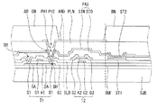
- 基板上の第1の領域に配置された第1の薄膜トランジスタと、
前記基板上の第2の領域に配置された第2の薄膜トランジスタと、
前記基板上の第3の領域に配置された第1の補助容量電極と、
前記第1の薄膜トランジスタ及び前記第2の薄膜トランジスタを覆い、前記第1の補助容量電極を露出する酸化膜と、
前記酸化膜上に積層され、前記第1の補助容量電極を覆う窒化膜と、
前記窒化膜上で前記第1の補助容量電極と重ね合わせられる第2の補助容量電極と、
前記第1の薄膜トランジスタ、前記第2の薄膜トランジスタ、及び前記第2の補助容量電極を覆う平坦化膜と、
前記平坦化膜上に配置された画素電極と、
を備える薄膜トランジスタ基板。 - 前記第1の薄膜トランジスタは、
第1の半導体層と、
前記第1の半導体層の中心部と重ね合わせられる第1のゲート電極と、
前記第1の半導体層の一側部と接触する第1のソース電極と、
前記第1の半導体層の他側部と接触する第1のドレイン電極と、
前記窒化膜と前記酸化膜を貫通して前記第1のドレイン電極を露出する第1の画素コンタクトホールと、
前記第1の画素コンタクトホールを介して前記第1のドレイン電極と接触する補助ドレイン電極と、
をさらに備え、
前記画素電極は、前記平坦化膜を貫通して前記補助ドレイン電極を露出する第2の画素コンタクトホールを介して前記補助ドレインと接触する請求項1に記載の薄膜トランジスタ基板。 - 前記補助ドレイン電極は、
前記第2の補助容量電極と同じ層に配置され、同じ物質を含む請求項2に記載の薄膜トランジスタ基板。 - 前記第2の薄膜トランジスタは、画素を選択するスイッチング素子であり、
前記第1の薄膜トランジスタは、前記第2の薄膜トランジスタにより選択された前記画素を駆動するための駆動素子である請求項1に記載の薄膜トランジスタ基板。 - 前記酸化膜は、3,000Å以上の厚さを有し、
前記窒化膜は、500〜3,000Åの厚さを有する請求項1に記載の薄膜トランジスタ基板。 - 前記第1の薄膜トランジスタ及び前記第2の薄膜トランジスタは、
多結晶半導体物質を含む第1の半導体層と、
前記第1の半導体層を覆うゲート絶縁膜と、
前記ゲート絶縁膜上で前記第1の半導体層と重ね合わせられる第1のゲート電極と、
前記ゲート絶縁膜上に配置された第2のゲート電極と、
前記第1のゲート電極と第2のゲート電極とを覆う中間絶縁膜と、
前記中間絶縁膜上で、前記第2のゲート電極と重ね合わせられるように配置され、酸化物半導体物質を含む第2の半導体層と、
前記中間絶縁膜上に配置された第1のソース電極及び第1のドレイン電極と、
前記第2の半導体層上に配置された第2のソース電極及び第2のドレイン電極と、
を備え、
前記第1の半導体層、前記第1のゲート電極、前記第1のソース電極、及び前記第1のドレイン電極は、前記第1の薄膜トランジスタに含まれ、
前記第2の半導体層、前記第2のゲート電極、前記第2のソース電極、及び前記第2のドレイン電極は、前記第2の薄膜トランジスタに含まれる請求項1に記載の薄膜トランジスタ基板。 - 前記第1の補助容量電極は、
前記ゲート絶縁膜上に積層された前記中間絶縁膜上に配置された請求項6に記載の薄膜トランジスタ基板。 - 前記第1の補助容量電極は、
前記第2のソース電極及び前記第2のドレイン電極と同じ層に配置され、同じ物質を含む請求項6に記載の薄膜トランジスタ基板。
Applications Claiming Priority (2)
| Application Number | Priority Date | Filing Date | Title |
|---|---|---|---|
| KR10-2015-0187565 | 2015-12-28 | ||
| KR1020150187565A KR102465559B1 (ko) | 2015-12-28 | 2015-12-28 | 박막 트랜지스터 기판 및 이를 이용한 표시장치 |
Publications (2)
| Publication Number | Publication Date |
|---|---|
| JP2017120893A true JP2017120893A (ja) | 2017-07-06 |
| JP6401228B2 JP6401228B2 (ja) | 2018-10-10 |
Family
ID=56235752
Family Applications (1)
| Application Number | Title | Priority Date | Filing Date |
|---|---|---|---|
| JP2016239163A Active JP6401228B2 (ja) | 2015-12-28 | 2016-12-09 | 薄膜トランジスタ基板 |
Country Status (5)
| Country | Link |
|---|---|
| US (1) | US9954014B2 (ja) |
| EP (1) | EP3188236A1 (ja) |
| JP (1) | JP6401228B2 (ja) |
| KR (1) | KR102465559B1 (ja) |
| CN (1) | CN106920802B (ja) |
Cited By (1)
| Publication number | Priority date | Publication date | Assignee | Title |
|---|---|---|---|---|
| WO2021166940A1 (ja) * | 2020-02-20 | 2021-08-26 | 株式会社ニコン | トランジスタ、電子デバイス及びトランジスタの製造方法 |
Families Citing this family (13)
| Publication number | Priority date | Publication date | Assignee | Title |
|---|---|---|---|---|
| CN106229297B (zh) * | 2016-09-18 | 2019-04-02 | 深圳市华星光电技术有限公司 | Amoled像素驱动电路的制作方法 |
| US10191345B2 (en) | 2016-11-01 | 2019-01-29 | Innolux Corporation | Display device |
| CN106935546B (zh) * | 2017-04-12 | 2019-09-06 | 京东方科技集团股份有限公司 | 阵列基板的制备方法、阵列基板、显示面板和显示装置 |
| CN107680993B (zh) * | 2017-10-23 | 2019-12-24 | 深圳市华星光电半导体显示技术有限公司 | Oled面板及其制作方法 |
| US11152551B2 (en) * | 2018-04-27 | 2021-10-19 | Innolux Corporation | Electronic device |
| KR102837792B1 (ko) | 2019-05-13 | 2025-07-23 | 삼성디스플레이 주식회사 | 디스플레이 패널 및 이를 포함하는 디스플레이 장치 |
| KR102727809B1 (ko) * | 2019-12-10 | 2024-11-07 | 엘지디스플레이 주식회사 | 폴더블 표시장치 |
| KR102836372B1 (ko) * | 2019-12-17 | 2025-07-18 | 엘지디스플레이 주식회사 | 표시장치 및 그 제조방법 |
| US12336349B2 (en) * | 2020-02-28 | 2025-06-17 | Samsung Display Co., Ltd. | Display device |
| CN111785759B (zh) * | 2020-07-17 | 2025-04-29 | 武汉华星光电半导体显示技术有限公司 | 显示面板及显示装置 |
| US11895870B2 (en) | 2020-07-17 | 2024-02-06 | Wuhan China Star Optoelectronics Semiconductor Display Technology Co., Ltd. | Display panel and display device |
| CN112530978B (zh) * | 2020-12-01 | 2024-02-13 | 京东方科技集团股份有限公司 | 开关器件结构及其制备方法、薄膜晶体管膜层、显示面板 |
| CN112713179A (zh) * | 2020-12-30 | 2021-04-27 | 深圳市华星光电半导体显示技术有限公司 | 显示面板及显示装置 |
Citations (8)
| Publication number | Priority date | Publication date | Assignee | Title |
|---|---|---|---|---|
| JP2002123192A (ja) * | 2000-10-18 | 2002-04-26 | Seiko Epson Corp | 電気光学装置及びその製造方法 |
| JP2002236460A (ja) * | 2001-02-08 | 2002-08-23 | Seiko Epson Corp | 電気光学装置及びその製造方法並びに投射型表示装置 |
| JP2005201963A (ja) * | 2004-01-13 | 2005-07-28 | Seiko Epson Corp | 電気光学装置、それを用いた電子機器、電気光学装置の製造方法 |
| JP2011040730A (ja) * | 2009-07-17 | 2011-02-24 | Semiconductor Energy Lab Co Ltd | 半導体装置及び半導体装置の作製方法 |
| JP2011076079A (ja) * | 2009-09-04 | 2011-04-14 | Semiconductor Energy Lab Co Ltd | 表示装置、および電子機器 |
| JP2014241403A (ja) * | 2013-05-16 | 2014-12-25 | 株式会社半導体エネルギー研究所 | 半導体装置 |
| JP2015034979A (ja) * | 2013-07-12 | 2015-02-19 | 株式会社半導体エネルギー研究所 | 表示装置および表示装置の作製方法 |
| US20150243685A1 (en) * | 2014-02-24 | 2015-08-27 | Lg Display Co., Ltd. | Thin film transistor substrate and display using the same |
Family Cites Families (9)
| Publication number | Priority date | Publication date | Assignee | Title |
|---|---|---|---|---|
| US7646367B2 (en) * | 2005-01-21 | 2010-01-12 | Semiconductor Energy Laboratory Co., Ltd. | Semiconductor device, display device and electronic apparatus |
| KR20120039947A (ko) * | 2010-10-18 | 2012-04-26 | 삼성모바일디스플레이주식회사 | 표시 장치 및 그 제조 방법 |
| KR101833235B1 (ko) * | 2011-07-14 | 2018-04-16 | 삼성디스플레이 주식회사 | 박막 트랜지스터 어레이 기판, 이를 포함하는 유기 발광 표시 장치 및 그 제조 방법 |
| US9368523B2 (en) * | 2012-03-27 | 2016-06-14 | Sharp Kabushiki Kaisha | Semiconductor device, method for manufacturing semiconductor device, and display device |
| KR102023185B1 (ko) * | 2013-07-08 | 2019-11-05 | 삼성디스플레이 주식회사 | 유기 발광 표시 장치 |
| WO2015052991A1 (ja) * | 2013-10-09 | 2015-04-16 | シャープ株式会社 | 半導体装置およびその製造方法 |
| EP2911202B1 (en) * | 2014-02-24 | 2019-02-20 | LG Display Co., Ltd. | Thin film transistor substrate and display using the same |
| KR102251177B1 (ko) * | 2014-02-24 | 2021-05-12 | 엘지디스플레이 주식회사 | 박막 트랜지스터 기판 및 이를 이용한 표시장치 |
| KR102457204B1 (ko) * | 2015-08-27 | 2022-10-21 | 엘지디스플레이 주식회사 | 박막 트랜지스터 기판 및 이를 이용한 표시장치 |
-
2015
- 2015-12-28 KR KR1020150187565A patent/KR102465559B1/ko active Active
-
2016
- 2016-06-27 EP EP16176330.5A patent/EP3188236A1/en not_active Withdrawn
- 2016-07-26 CN CN201610596661.4A patent/CN106920802B/zh active Active
- 2016-08-24 US US15/245,944 patent/US9954014B2/en active Active
- 2016-12-09 JP JP2016239163A patent/JP6401228B2/ja active Active
Patent Citations (8)
| Publication number | Priority date | Publication date | Assignee | Title |
|---|---|---|---|---|
| JP2002123192A (ja) * | 2000-10-18 | 2002-04-26 | Seiko Epson Corp | 電気光学装置及びその製造方法 |
| JP2002236460A (ja) * | 2001-02-08 | 2002-08-23 | Seiko Epson Corp | 電気光学装置及びその製造方法並びに投射型表示装置 |
| JP2005201963A (ja) * | 2004-01-13 | 2005-07-28 | Seiko Epson Corp | 電気光学装置、それを用いた電子機器、電気光学装置の製造方法 |
| JP2011040730A (ja) * | 2009-07-17 | 2011-02-24 | Semiconductor Energy Lab Co Ltd | 半導体装置及び半導体装置の作製方法 |
| JP2011076079A (ja) * | 2009-09-04 | 2011-04-14 | Semiconductor Energy Lab Co Ltd | 表示装置、および電子機器 |
| JP2014241403A (ja) * | 2013-05-16 | 2014-12-25 | 株式会社半導体エネルギー研究所 | 半導体装置 |
| JP2015034979A (ja) * | 2013-07-12 | 2015-02-19 | 株式会社半導体エネルギー研究所 | 表示装置および表示装置の作製方法 |
| US20150243685A1 (en) * | 2014-02-24 | 2015-08-27 | Lg Display Co., Ltd. | Thin film transistor substrate and display using the same |
Cited By (3)
| Publication number | Priority date | Publication date | Assignee | Title |
|---|---|---|---|---|
| WO2021166940A1 (ja) * | 2020-02-20 | 2021-08-26 | 株式会社ニコン | トランジスタ、電子デバイス及びトランジスタの製造方法 |
| JPWO2021166940A1 (ja) * | 2020-02-20 | 2021-08-26 | ||
| JP7657767B2 (ja) | 2020-02-20 | 2025-04-07 | 株式会社ニコン | トランジスタ、電子デバイス及びトランジスタの製造方法 |
Also Published As
| Publication number | Publication date |
|---|---|
| EP3188236A1 (en) | 2017-07-05 |
| KR20170077920A (ko) | 2017-07-07 |
| US9954014B2 (en) | 2018-04-24 |
| KR102465559B1 (ko) | 2022-11-11 |
| CN106920802B (zh) | 2019-09-17 |
| JP6401228B2 (ja) | 2018-10-10 |
| CN106920802A (zh) | 2017-07-04 |
| US20170186781A1 (en) | 2017-06-29 |
Similar Documents
| Publication | Publication Date | Title |
|---|---|---|
| JP6401228B2 (ja) | 薄膜トランジスタ基板 | |
| KR102457204B1 (ko) | 박막 트랜지스터 기판 및 이를 이용한 표시장치 | |
| KR102437650B1 (ko) | 박막 트랜지스터 기판 및 이를 이용한 표시장치 | |
| US10714557B2 (en) | Substrate for display device and display device including the same | |
| US10692893B2 (en) | Substrate for display device and display device including the same | |
| CN204464286U (zh) | 显示装置 | |
| KR102326170B1 (ko) | 박막 트랜지스터 기판 및 그 제조 방법 | |
| CN204538024U (zh) | 薄膜晶体管基板 | |
| KR102349595B1 (ko) | 박막 트랜지스터 기판 및 이를 이용한 표시장치 | |
| US10361229B2 (en) | Display device | |
| CN104867935B (zh) | 薄膜晶体管基板及利用该薄膜晶体管基板的显示装置 | |
| KR102454087B1 (ko) | 박막 트랜지스터 기판 | |
| KR20170061778A (ko) | 유기발광 다이오드 표시장치용 박막 트랜지스터 기판 | |
| KR20160103492A (ko) | 박막 트랜지스터 기판 및 이를 이용한 표시장치 | |
| CN118102790A (zh) | 包括氧化物半导体的显示装置 |
Legal Events
| Date | Code | Title | Description |
|---|---|---|---|
| A977 | Report on retrieval |
Free format text: JAPANESE INTERMEDIATE CODE: A971007 Effective date: 20171010 |
|
| A131 | Notification of reasons for refusal |
Free format text: JAPANESE INTERMEDIATE CODE: A131 Effective date: 20171017 |
|
| A601 | Written request for extension of time |
Free format text: JAPANESE INTERMEDIATE CODE: A601 Effective date: 20180117 |
|
| A601 | Written request for extension of time |
Free format text: JAPANESE INTERMEDIATE CODE: A601 Effective date: 20180316 |
|
| A521 | Request for written amendment filed |
Free format text: JAPANESE INTERMEDIATE CODE: A523 Effective date: 20180409 |
|
| RD03 | Notification of appointment of power of attorney |
Free format text: JAPANESE INTERMEDIATE CODE: A7423 Effective date: 20180531 |
|
| RD04 | Notification of resignation of power of attorney |
Free format text: JAPANESE INTERMEDIATE CODE: A7424 Effective date: 20180612 |
|
| TRDD | Decision of grant or rejection written | ||
| RD04 | Notification of resignation of power of attorney |
Free format text: JAPANESE INTERMEDIATE CODE: A7424 Effective date: 20180704 |
|
| A01 | Written decision to grant a patent or to grant a registration (utility model) |
Free format text: JAPANESE INTERMEDIATE CODE: A01 Effective date: 20180809 |
|
| A61 | First payment of annual fees (during grant procedure) |
Free format text: JAPANESE INTERMEDIATE CODE: A61 Effective date: 20180906 |
|
| R150 | Certificate of patent or registration of utility model |
Ref document number: 6401228 Country of ref document: JP Free format text: JAPANESE INTERMEDIATE CODE: R150 |
|
| R250 | Receipt of annual fees |
Free format text: JAPANESE INTERMEDIATE CODE: R250 |
|
| R250 | Receipt of annual fees |
Free format text: JAPANESE INTERMEDIATE CODE: R250 |
|
| R250 | Receipt of annual fees |
Free format text: JAPANESE INTERMEDIATE CODE: R250 |
|
| R250 | Receipt of annual fees |
Free format text: JAPANESE INTERMEDIATE CODE: R250 |
|
| R250 | Receipt of annual fees |
Free format text: JAPANESE INTERMEDIATE CODE: R250 |