JP2017135218A - 荷電粒子ビームレンズ装置、荷電粒子ビームカラム、および荷電粒子ビーム露光装置 - Google Patents
荷電粒子ビームレンズ装置、荷電粒子ビームカラム、および荷電粒子ビーム露光装置 Download PDFInfo
- Publication number
- JP2017135218A JP2017135218A JP2016012798A JP2016012798A JP2017135218A JP 2017135218 A JP2017135218 A JP 2017135218A JP 2016012798 A JP2016012798 A JP 2016012798A JP 2016012798 A JP2016012798 A JP 2016012798A JP 2017135218 A JP2017135218 A JP 2017135218A
- Authority
- JP
- Japan
- Prior art keywords
- lens
- charged particle
- particle beam
- electron beam
- unit
- Prior art date
- Legal status (The legal status is an assumption and is not a legal conclusion. Google has not performed a legal analysis and makes no representation as to the accuracy of the status listed.)
- Withdrawn
Links
Images






Classifications
-
- H—ELECTRICITY
- H01—ELECTRIC ELEMENTS
- H01J—ELECTRIC DISCHARGE TUBES OR DISCHARGE LAMPS
- H01J37/00—Discharge tubes with provision for introducing objects or material to be exposed to the discharge, e.g. for the purpose of examination or processing thereof
- H01J37/02—Details
- H01J37/04—Arrangements of electrodes and associated parts for generating or controlling the discharge, e.g. electron-optical arrangement or ion-optical arrangement
- H01J37/10—Lenses
- H01J37/14—Lenses magnetic
-
- G—PHYSICS
- G03—PHOTOGRAPHY; CINEMATOGRAPHY; ANALOGOUS TECHNIQUES USING WAVES OTHER THAN OPTICAL WAVES; ELECTROGRAPHY; HOLOGRAPHY
- G03F—PHOTOMECHANICAL PRODUCTION OF TEXTURED OR PATTERNED SURFACES, e.g. FOR PRINTING, FOR PROCESSING OF SEMICONDUCTOR DEVICES; MATERIALS THEREFOR; ORIGINALS THEREFOR; APPARATUS SPECIALLY ADAPTED THEREFOR
- G03F7/00—Photomechanical, e.g. photolithographic, production of textured or patterned surfaces, e.g. printing surfaces; Materials therefor, e.g. comprising photoresists; Apparatus specially adapted therefor
- G03F7/70—Microphotolithographic exposure; Apparatus therefor
- G03F7/70216—Mask projection systems
- G03F7/70275—Multiple projection paths, e.g. array of projection systems, microlens projection systems or tandem projection systems
-
- H—ELECTRICITY
- H01—ELECTRIC ELEMENTS
- H01J—ELECTRIC DISCHARGE TUBES OR DISCHARGE LAMPS
- H01J37/00—Discharge tubes with provision for introducing objects or material to be exposed to the discharge, e.g. for the purpose of examination or processing thereof
- H01J37/02—Details
- H01J37/04—Arrangements of electrodes and associated parts for generating or controlling the discharge, e.g. electron-optical arrangement or ion-optical arrangement
- H01J37/10—Lenses
- H01J37/14—Lenses magnetic
- H01J37/141—Electromagnetic lenses
-
- G—PHYSICS
- G03—PHOTOGRAPHY; CINEMATOGRAPHY; ANALOGOUS TECHNIQUES USING WAVES OTHER THAN OPTICAL WAVES; ELECTROGRAPHY; HOLOGRAPHY
- G03F—PHOTOMECHANICAL PRODUCTION OF TEXTURED OR PATTERNED SURFACES, e.g. FOR PRINTING, FOR PROCESSING OF SEMICONDUCTOR DEVICES; MATERIALS THEREFOR; ORIGINALS THEREFOR; APPARATUS SPECIALLY ADAPTED THEREFOR
- G03F1/00—Originals for photomechanical production of textured or patterned surfaces, e.g., masks, photo-masks, reticles; Mask blanks or pellicles therefor; Containers specially adapted therefor; Preparation thereof
- G03F1/20—Masks or mask blanks for imaging by charged particle beam [CPB] radiation, e.g. by electron beam; Preparation thereof
-
- G—PHYSICS
- G03—PHOTOGRAPHY; CINEMATOGRAPHY; ANALOGOUS TECHNIQUES USING WAVES OTHER THAN OPTICAL WAVES; ELECTROGRAPHY; HOLOGRAPHY
- G03F—PHOTOMECHANICAL PRODUCTION OF TEXTURED OR PATTERNED SURFACES, e.g. FOR PRINTING, FOR PROCESSING OF SEMICONDUCTOR DEVICES; MATERIALS THEREFOR; ORIGINALS THEREFOR; APPARATUS SPECIALLY ADAPTED THEREFOR
- G03F7/00—Photomechanical, e.g. photolithographic, production of textured or patterned surfaces, e.g. printing surfaces; Materials therefor, e.g. comprising photoresists; Apparatus specially adapted therefor
- G03F7/70—Microphotolithographic exposure; Apparatus therefor
- G03F7/708—Construction of apparatus, e.g. environment aspects, hygiene aspects or materials
- G03F7/70808—Construction details, e.g. housing, load-lock, seals or windows for passing light in or out of apparatus
- G03F7/70833—Mounting of optical systems, e.g. mounting of illumination system, projection system or stage systems on base-plate or ground
-
- H—ELECTRICITY
- H01—ELECTRIC ELEMENTS
- H01J—ELECTRIC DISCHARGE TUBES OR DISCHARGE LAMPS
- H01J37/00—Discharge tubes with provision for introducing objects or material to be exposed to the discharge, e.g. for the purpose of examination or processing thereof
- H01J37/02—Details
- H01J37/04—Arrangements of electrodes and associated parts for generating or controlling the discharge, e.g. electron-optical arrangement or ion-optical arrangement
- H01J37/06—Electron sources; Electron guns
- H01J37/07—Eliminating deleterious effects due to thermal effects or electric or magnetic fields
-
- H—ELECTRICITY
- H01—ELECTRIC ELEMENTS
- H01J—ELECTRIC DISCHARGE TUBES OR DISCHARGE LAMPS
- H01J37/00—Discharge tubes with provision for introducing objects or material to be exposed to the discharge, e.g. for the purpose of examination or processing thereof
- H01J37/30—Electron-beam or ion-beam tubes for localised treatment of objects
- H01J37/317—Electron-beam or ion-beam tubes for localised treatment of objects for changing properties of the objects or for applying thin layers thereon, e.g. for ion implantation
- H01J37/3174—Particle-beam lithography, e.g. electron beam lithography
-
- H—ELECTRICITY
- H01—ELECTRIC ELEMENTS
- H01J—ELECTRIC DISCHARGE TUBES OR DISCHARGE LAMPS
- H01J37/00—Discharge tubes with provision for introducing objects or material to be exposed to the discharge, e.g. for the purpose of examination or processing thereof
- H01J37/30—Electron-beam or ion-beam tubes for localised treatment of objects
- H01J37/317—Electron-beam or ion-beam tubes for localised treatment of objects for changing properties of the objects or for applying thin layers thereon, e.g. for ion implantation
- H01J37/3174—Particle-beam lithography, e.g. electron beam lithography
- H01J37/3177—Multi-beam, e.g. fly's eye, comb probe
-
- H—ELECTRICITY
- H01—ELECTRIC ELEMENTS
- H01J—ELECTRIC DISCHARGE TUBES OR DISCHARGE LAMPS
- H01J2237/00—Discharge tubes exposing object to beam, e.g. for analysis treatment, etching, imaging
- H01J2237/002—Cooling arrangements
-
- H—ELECTRICITY
- H01—ELECTRIC ELEMENTS
- H01J—ELECTRIC DISCHARGE TUBES OR DISCHARGE LAMPS
- H01J2237/00—Discharge tubes exposing object to beam, e.g. for analysis treatment, etching, imaging
- H01J2237/10—Lenses
- H01J2237/14—Lenses magnetic
- H01J2237/1405—Constructional details
-
- H—ELECTRICITY
- H01—ELECTRIC ELEMENTS
- H01J—ELECTRIC DISCHARGE TUBES OR DISCHARGE LAMPS
- H01J2237/00—Discharge tubes exposing object to beam, e.g. for analysis treatment, etching, imaging
- H01J2237/20—Positioning, supporting, modifying or maintaining the physical state of objects being observed or treated
- H01J2237/202—Movement
- H01J2237/20278—Motorised movement
- H01J2237/20285—Motorised movement computer-controlled
-
- H—ELECTRICITY
- H01—ELECTRIC ELEMENTS
- H01J—ELECTRIC DISCHARGE TUBES OR DISCHARGE LAMPS
- H01J2237/00—Discharge tubes exposing object to beam, e.g. for analysis treatment, etching, imaging
- H01J2237/30—Electron or ion beam tubes for processing objects
- H01J2237/317—Processing objects on a microscale
- H01J2237/3175—Lithography
- H01J2237/31774—Multi-beam
Landscapes
- Chemical & Material Sciences (AREA)
- Analytical Chemistry (AREA)
- Physics & Mathematics (AREA)
- General Physics & Mathematics (AREA)
- Electromagnetism (AREA)
- Health & Medical Sciences (AREA)
- Engineering & Computer Science (AREA)
- Environmental & Geological Engineering (AREA)
- Epidemiology (AREA)
- Public Health (AREA)
- Electron Beam Exposure (AREA)
Abstract
Description
特許文献1 特開2013−16744号公報
特許文献2 特開昭61−227356号公報
特許文献3 特開2014−120545号公報
非特許文献1 Proc. SPIE 7637, Alternative Lithographic Technologies II, 76370C (March 10, 2010).
(数1)
V=4×U/(πD2)
(数2)
Re=V×D/(μ/ρ)
(数3)
P=λ×(L/d)×(1/2)×(ρ×V2)
(数4)
λ=64/Re
Claims (14)
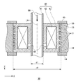
- 荷電粒子ビームを通過させる貫通孔の周囲に形成され、前記荷電粒子ビームを収束または拡散させるレンズ部と、
前記レンズ部の外周を囲む支持部と、
を備え、
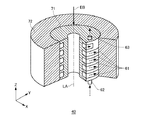
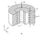
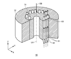
前記レンズ部における前記支持部と接する外周部分および前記支持部における前記レンズ部と接する内周部分の少なくとも一方は、前記レンズ部の外周に沿って冷却用流体を流すための溝部を有する
荷電粒子ビームレンズ装置。 - 荷電粒子ビームを通過させる貫通孔の周囲に形成され、前記荷電粒子ビームを収束または拡散させるレンズ部と、
前記レンズ部の外周を囲む支持部と、
を備え、
前記レンズ部は、
前記貫通孔の周囲に形成される第1部材と、
前記第1部材の外周を囲む第2部材と、
を有し、
前記第1部材における前記第2部材と接する外周部分および前記第2部材における前記第1部材と接する内周部分の少なくとも一方は、前記第1部材の外周に沿って冷却用流体を流すための溝部を有する
荷電粒子ビームレンズ装置。 - 前記外周部分および前記内周部分は、前記貫通孔の延伸方向と平行な面の少なくとも一部である請求項1または2に記載の荷電粒子ビームレンズ装置。
- 前記溝部は、前記貫通孔の中心軸を通る面に対して対称に形成される請求項1から3のいずれか一項に記載の荷電粒子ビームレンズ装置。
- 前記溝部の一端と接続する流入部と、
前記溝部の他端と接続する排出部と、
を備え、
前記溝部は、前記流入部から流入する冷却用流体を前記排出部から排出する請求項1から4のいずれか一項に記載の荷電粒子ビームレンズ装置。 - 前記流入部は、前記レンズ部の、前記荷電粒子ビームが出射する側に形成され、
前記排出部は、前記レンズ部の、前記荷電粒子ビームが入射する側に形成される請求項5に記載の荷電粒子ビームレンズ装置。 - 前記流入部に接続され、前記流入部から冷却用流体を供給する流入側流体槽と、
前記排出部に接続され、前記排出部から前記溝部を通過した冷却用流体を排出する排出側流体槽と、を備える請求項5または6に記載の荷電粒子ビームレンズ装置。 - 複数の前記溝部と、複数の前記溝部のそれぞれに対応する複数の前記流入部および複数の前記排出部を備える請求項5から7のいずれか一項に記載の荷電粒子ビームレンズ装置。
- 前記レンズ部は、前記貫通孔の延伸方向と平行な中心軸を有する円柱形状に形成され、外径が22mm以上30mm以内である請求項1から8のいずれか一項に記載の荷電粒子ビームレンズ装置。
- 前記溝部は、水を主成分とする冷却水を前記冷却用流体として流す請求項1から9のいずれか一項に記載の荷電粒子ビームレンズ装置。
- 前記溝部は、断面積が0.5mm2以上1mm2以下であり、長さが0.7m以上1.5m以下である、請求項10に記載の荷電粒子ビームレンズ装置。
- 前記レンズ部は、
前記貫通孔を形成する障壁部と、
前記貫通孔の延伸方向の磁場を発生させる励磁部と、
前記励磁部が発生させた磁場の方向を調節する磁性体部と、
を有し、
前記第1部材および前記第2部材は、前記障壁部、前記励磁部、および前記磁性体部のうち、少なくとも1つを形成する請求項2に記載の荷電粒子ビームレンズ装置。 - 荷電粒子ビームを放出する粒子源と、
請求項1から12のいずれか一項に記載の荷電粒子ビームレンズ装置と、
を有する荷電粒子ビームカラム。 - 請求項13に記載の荷電粒子ビームカラムを1または複数備える荷電粒子ビーム露光装置。
Priority Applications (7)
| Application Number | Priority Date | Filing Date | Title |
|---|---|---|---|
| JP2016012798A JP2017135218A (ja) | 2016-01-26 | 2016-01-26 | 荷電粒子ビームレンズ装置、荷電粒子ビームカラム、および荷電粒子ビーム露光装置 |
| EP16195044.9A EP3200216A1 (en) | 2016-01-26 | 2016-10-21 | Charged particle beam lens apparatus, charged particle beam column, and charged particle beam exposure apparatus |
| TW107123125A TW201907435A (zh) | 2016-01-26 | 2016-10-24 | 帶電粒子束透鏡裝置、帶電粒子束柱體、及帶電粒子束曝光裝置(二) |
| TW105134224A TWI632586B (zh) | 2016-01-26 | 2016-10-24 | Charged particle beam lens device, charged particle beam cylinder, and charged particle beam exposure device |
| US15/335,448 US10049854B2 (en) | 2016-01-26 | 2016-10-27 | Charged particle beam lens apparatus, charged particle beam column, and charged particle beam exposure apparatus |
| KR1020160141442A KR101877633B1 (ko) | 2016-01-26 | 2016-10-27 | 하전 입자 빔 렌즈 장치, 하전 입자 빔 컬럼 및 하전 입자 빔 노광 장치 |
| CN201610958663.3A CN107017142A (zh) | 2016-01-26 | 2016-10-28 | 带电粒子束透镜装置、带电粒子束柱及带电粒子束曝光装置 |
Applications Claiming Priority (1)
| Application Number | Priority Date | Filing Date | Title |
|---|---|---|---|
| JP2016012798A JP2017135218A (ja) | 2016-01-26 | 2016-01-26 | 荷電粒子ビームレンズ装置、荷電粒子ビームカラム、および荷電粒子ビーム露光装置 |
Publications (1)
| Publication Number | Publication Date |
|---|---|
| JP2017135218A true JP2017135218A (ja) | 2017-08-03 |
Family
ID=57206039
Family Applications (1)
| Application Number | Title | Priority Date | Filing Date |
|---|---|---|---|
| JP2016012798A Withdrawn JP2017135218A (ja) | 2016-01-26 | 2016-01-26 | 荷電粒子ビームレンズ装置、荷電粒子ビームカラム、および荷電粒子ビーム露光装置 |
Country Status (6)
| Country | Link |
|---|---|
| US (1) | US10049854B2 (ja) |
| EP (1) | EP3200216A1 (ja) |
| JP (1) | JP2017135218A (ja) |
| KR (1) | KR101877633B1 (ja) |
| CN (1) | CN107017142A (ja) |
| TW (2) | TWI632586B (ja) |
Cited By (1)
| Publication number | Priority date | Publication date | Assignee | Title |
|---|---|---|---|---|
| JP2023014010A (ja) * | 2021-07-14 | 2023-01-26 | アイエムエス ナノファブリケーション ゲーエムベーハー | 電磁レンズ及び荷電粒子光学装置 |
Families Citing this family (4)
| Publication number | Priority date | Publication date | Assignee | Title |
|---|---|---|---|---|
| EP3528273B1 (de) * | 2018-02-20 | 2023-08-23 | Bühler AG | Vorrichtung und verfahren zum pasteurisieren und/oder sterilisieren von partikelförmigem gut |
| WO2020108984A2 (en) | 2018-11-30 | 2020-06-04 | Asml Netherlands B.V. | Systems and methods of cooling objective lens of a charged-particle beam system |
| US20220410275A1 (en) * | 2021-06-24 | 2022-12-29 | Wisconsin Alumni Research Foundation | High Energy 3-D Printer Employing Continuous Print Path |
| US12462968B2 (en) | 2021-10-29 | 2025-11-04 | Kla Corporation | Systems and methods for uniform cooling of electromagnetic coil |
Family Cites Families (16)
| Publication number | Priority date | Publication date | Assignee | Title |
|---|---|---|---|---|
| JPS57140169A (en) * | 1981-02-25 | 1982-08-30 | Toshiba Corp | Pressure pulse type ink jet recorder |
| JPS57140169U (ja) * | 1981-02-27 | 1982-09-02 | ||
| JPS60245132A (ja) * | 1984-05-21 | 1985-12-04 | Toshiba Corp | 電子ビ−ム露光装置等の電子レンズ |
| JPS61227356A (ja) | 1985-04-01 | 1986-10-09 | Hitachi Ltd | 荷電粒子線応用装置の冷却装置 |
| JP2002206833A (ja) * | 2001-01-05 | 2002-07-26 | Nikon Corp | 液体冷却系の振動低減方法、荷電粒子線露光装置及び半導体デバイスの製造方法 |
| US20020148971A1 (en) * | 2001-03-05 | 2002-10-17 | Michael Sogard | Lens assembly for electron beam column |
| JP2003115443A (ja) * | 2001-10-04 | 2003-04-18 | Nikon Corp | 荷電粒子線露光装置の鏡筒 |
| US7334898B2 (en) | 2003-10-10 | 2008-02-26 | Seiko Epson Corporation | Projector |
| JP4719628B2 (ja) * | 2006-06-13 | 2011-07-06 | 株式会社日立ハイテクノロジーズ | 走査電子顕微鏡 |
| WO2012041464A1 (en) * | 2010-09-28 | 2012-04-05 | Applied Materials Israel Ltd. | Particle-optical systems and arrangements and particle-optical components for such systems and arrangements |
| CN103038855B (zh) * | 2010-10-27 | 2016-02-03 | 株式会社Param | 电子透镜和电子束装置 |
| EP2511939B1 (en) * | 2011-04-13 | 2016-03-23 | ICT Integrated Circuit Testing Gesellschaft für Halbleiterprüftechnik mbH | Arrangement and method for the contrast improvement in a charged particle beam device for inspecting a specimen |
| JP2013016744A (ja) | 2011-07-06 | 2013-01-24 | Canon Inc | 描画装置及びデバイスの製造方法 |
| CN107359101B (zh) * | 2012-05-14 | 2019-07-12 | Asml荷兰有限公司 | 带电粒子射束产生器中的高电压屏蔽和冷却 |
| JP5667618B2 (ja) | 2012-12-14 | 2015-02-12 | 株式会社アドバンテスト | 電磁レンズ及び電子ビーム露光装置 |
| JP6161430B2 (ja) * | 2013-06-25 | 2017-07-12 | 株式会社日立ハイテクノロジーズ | 電子レンズ及び荷電粒子線装置 |
-
2016
- 2016-01-26 JP JP2016012798A patent/JP2017135218A/ja not_active Withdrawn
- 2016-10-21 EP EP16195044.9A patent/EP3200216A1/en not_active Withdrawn
- 2016-10-24 TW TW105134224A patent/TWI632586B/zh not_active IP Right Cessation
- 2016-10-24 TW TW107123125A patent/TW201907435A/zh unknown
- 2016-10-27 KR KR1020160141442A patent/KR101877633B1/ko not_active Expired - Fee Related
- 2016-10-27 US US15/335,448 patent/US10049854B2/en active Active
- 2016-10-28 CN CN201610958663.3A patent/CN107017142A/zh active Pending
Cited By (2)
| Publication number | Priority date | Publication date | Assignee | Title |
|---|---|---|---|---|
| JP2023014010A (ja) * | 2021-07-14 | 2023-01-26 | アイエムエス ナノファブリケーション ゲーエムベーハー | 電磁レンズ及び荷電粒子光学装置 |
| JP7771004B2 (ja) | 2021-07-14 | 2025-11-17 | アイエムエス ナノファブリケーション ゲーエムベーハー | 電磁レンズ及び荷電粒子光学装置 |
Also Published As
| Publication number | Publication date |
|---|---|
| US20170213689A1 (en) | 2017-07-27 |
| KR20170089394A (ko) | 2017-08-03 |
| CN107017142A (zh) | 2017-08-04 |
| TW201907435A (zh) | 2019-02-16 |
| EP3200216A1 (en) | 2017-08-02 |
| TW201727690A (zh) | 2017-08-01 |
| KR101877633B1 (ko) | 2018-07-12 |
| TWI632586B (zh) | 2018-08-11 |
| US10049854B2 (en) | 2018-08-14 |
Similar Documents
| Publication | Publication Date | Title |
|---|---|---|
| JP2017135218A (ja) | 荷電粒子ビームレンズ装置、荷電粒子ビームカラム、および荷電粒子ビーム露光装置 | |
| JP5295423B2 (ja) | ホールスラスタ及び宇宙航行体及び推進方法 | |
| JP4509781B2 (ja) | 注入装置のリボン形状イオンビームの特性制御 | |
| CN103038855B (zh) | 电子透镜和电子束装置 | |
| JP6233617B2 (ja) | アークプラズマ成膜装置 | |
| KR101961914B1 (ko) | 하전 입자 리소그래피 시스템 및 빔 생성기 | |
| CN106660270A (zh) | 使用激光与等离子体的增材制造 | |
| JP6480534B1 (ja) | 荷電粒子ビーム照射装置及び基板の帯電低減方法 | |
| JP6446133B2 (ja) | アクチュエータ、位置決め装置、リソグラフィ装置、およびアクチュエータの製造方法 | |
| KR20170036479A (ko) | 이온 빔 에칭 장치 | |
| KR20190100075A (ko) | 이온 빔 에칭을 위한 플라즈마 브릿지 중화기 | |
| KR101297291B1 (ko) | 슬릿 전극 및 이것을 구비한 하전 입자빔 발생장치 | |
| US10083813B2 (en) | Multicolumn charged particle beam exposure apparatus | |
| JP2009278001A (ja) | 荷電ビーム描画装置 | |
| JP2002139758A (ja) | 光短波長化装置 | |
| JP2008053116A (ja) | イオンガン、及び成膜装置 | |
| Bakeev et al. | Focused electron beam transport through a long narrow metal tube at elevated pressures in the forevacuum range | |
| JP2009058281A (ja) | エネルギ線照射装置 | |
| CN121687601A (zh) | 双脉冲限域离子流方向筛选装置及方法 | |
| JPH118098A (ja) | 加速管の温度調節システム | |
| Kastelewicz et al. | linearen Plasmagenerator PSI-1 |
Legal Events
| Date | Code | Title | Description |
|---|---|---|---|
| A711 | Notification of change in applicant |
Free format text: JAPANESE INTERMEDIATE CODE: A711 Effective date: 20170529 |
|
| A521 | Request for written amendment filed |
Free format text: JAPANESE INTERMEDIATE CODE: A821 Effective date: 20170529 |
|
| A711 | Notification of change in applicant |
Free format text: JAPANESE INTERMEDIATE CODE: A711 Effective date: 20181115 |
|
| A621 | Written request for application examination |
Free format text: JAPANESE INTERMEDIATE CODE: A621 Effective date: 20181213 |
|
| A761 | Written withdrawal of application |
Free format text: JAPANESE INTERMEDIATE CODE: A761 Effective date: 20190226 |