JP2017143247A - Semiconductor device with integrated magnetic tunnel junction - Google Patents
Semiconductor device with integrated magnetic tunnel junction Download PDFInfo
- Publication number
- JP2017143247A JP2017143247A JP2016246877A JP2016246877A JP2017143247A JP 2017143247 A JP2017143247 A JP 2017143247A JP 2016246877 A JP2016246877 A JP 2016246877A JP 2016246877 A JP2016246877 A JP 2016246877A JP 2017143247 A JP2017143247 A JP 2017143247A
- Authority
- JP
- Japan
- Prior art keywords
- layer
- metal layer
- metal
- dielectric
- semiconductor device
- Prior art date
- Legal status (The legal status is an assumption and is not a legal conclusion. Google has not performed a legal analysis and makes no representation as to the accuracy of the status listed.)
- Pending
Links
Images


Classifications
-
- H—ELECTRICITY
- H10—SEMICONDUCTOR DEVICES; ELECTRIC SOLID-STATE DEVICES NOT OTHERWISE PROVIDED FOR
- H10N—ELECTRIC SOLID-STATE DEVICES NOT OTHERWISE PROVIDED FOR
- H10N50/00—Galvanomagnetic devices
- H10N50/10—Magnetoresistive devices
-
- H—ELECTRICITY
- H10—SEMICONDUCTOR DEVICES; ELECTRIC SOLID-STATE DEVICES NOT OTHERWISE PROVIDED FOR
- H10N—ELECTRIC SOLID-STATE DEVICES NOT OTHERWISE PROVIDED FOR
- H10N50/00—Galvanomagnetic devices
- H10N50/01—Manufacture or treatment
-
- H—ELECTRICITY
- H10—SEMICONDUCTOR DEVICES; ELECTRIC SOLID-STATE DEVICES NOT OTHERWISE PROVIDED FOR
- H10N—ELECTRIC SOLID-STATE DEVICES NOT OTHERWISE PROVIDED FOR
- H10N50/00—Galvanomagnetic devices
- H10N50/80—Constructional details
Landscapes
- Engineering & Computer Science (AREA)
- Manufacturing & Machinery (AREA)
- Mram Or Spin Memory Techniques (AREA)
- Hall/Mr Elements (AREA)
- Internal Circuitry In Semiconductor Integrated Circuit Devices (AREA)
Abstract
【課題】組み込まれた磁気トンネル接合を有する半導体デバイス及びその製造方法を提供する。【解決手段】半導体デバイス100は、第1金属層110と、第1誘電体層120と、第2金属層130と、第2誘電体層140と、第3金属層150とのスタックを含む。更に、磁気トンネル接合(MTJ)デバイス160は、第1誘電体層および第2金属層の中に配置され、第1金属層および第3金属層に電気的に接続されている。【選択図】図1A semiconductor device having an incorporated magnetic tunnel junction and a method for manufacturing the same are provided. A semiconductor device includes a stack of a first metal layer, a first dielectric layer, a second metal layer, a second dielectric layer, and a third metal layer. In addition, a magnetic tunnel junction (MTJ) device 160 is disposed in the first dielectric layer and the second metal layer and is electrically connected to the first metal layer and the third metal layer. [Selection] Figure 1
Description
本発明は、一般的に磁気トンネル接合(MTJ)を有する半導体デバイスの分野に関し、特に半導体デバイスの誘電体層および金属層へのMTJの組込みに関する。 The present invention relates generally to the field of semiconductor devices having magnetic tunnel junctions (MTJs), and more particularly to incorporating MTJs into dielectric and metal layers of semiconductor devices.
埋込型スタティックランダムアクセスメモリ(SRAM)の代替品として、磁気抵抗ランダムアクセスメモリ(MRAM)デバイスへの関心が高まっている。MRAMデバイスは、磁気トンネル接合(MTJ)デバイスにおけるデータの不揮発性記憶のために使用することができる。MTJデバイスは、バックエンドオブライン(BEOL)処理で誘電体層内に形成され、金属層によって相互接続されて所望の電気回路を形成する。BEOL処理は、誘電体層によって分離され、誘電体材料によって隔離された相互接続ワイヤまたは配線を有する金属層を形成することを含む。更に、ビア接続部は、金属層を互いに接続するように形成される。 There is increasing interest in magnetoresistive random access memory (MRAM) devices as an alternative to embedded static random access memory (SRAM). MRAM devices can be used for non-volatile storage of data in magnetic tunnel junction (MTJ) devices. MTJ devices are formed in a dielectric layer by back-end-of-line (BEOL) processing and are interconnected by metal layers to form the desired electrical circuit. The BEOL process involves forming a metal layer having interconnect wires or wiring separated by a dielectric layer and separated by a dielectric material. Furthermore, the via connection portion is formed so as to connect the metal layers to each other.
より高いメモリ密度のより小型で高速な半導体デバイスに対する要求が常に増しているので、より高度な電気配線を有する改良された半導体デバイスに対する要求がある。 As the demand for smaller and faster semiconductor devices with higher memory density is constantly increasing, there is a need for improved semiconductor devices with higher electrical wiring.
本発明の具体例の少なくともいくつかの目的は、MTJデバイスがBEOLにおいて、特により高度なテクノロジノードに関連して、より効率的に組み込まれることができる改良された半導体デバイスを提供することである。 At least some objectives of embodiments of the present invention are to provide improved semiconductor devices in which MTJ devices can be more efficiently incorporated in BEOL, particularly in connection with higher technology nodes. .
本発明のこの目的および他の目的の少なくとも1つは、独立請求項に規定された特徴を有する半導体デバイスおよび方法を用いて達成される。発明の好適な具体例は、従属請求項によって特徴付けられる。 This and other objects of the invention are achieved using a semiconductor device and method having the features defined in the independent claims. Preferred embodiments of the invention are characterized by the dependent claims.
本発明の第1態様によると、半導体デバイスが提供される。半導体デバイスは、第1金属層と、第1金属層の上に配置された第1誘電体層と、第1誘電体層の上に配置された第2金属層と、第2金属層の上に配置された第2誘電体層と、第2誘電体層の上に配置された第3金属層とを含む。第1金属層は、第1誘電体層に配置されたビアによって第2金属層に電気的に接続され、第2金属層は、第2誘電体層に配置されたビアによって第3金属層に電気的に接続されている。更に、磁気トンネル接合(MTJ)を含む半導体デバイスは、第1誘電体層および第2金属層に配置され、第1金属層および第3金属層に電気的に接続されている。 According to a first aspect of the invention, a semiconductor device is provided. The semiconductor device includes a first metal layer, a first dielectric layer disposed on the first metal layer, a second metal layer disposed on the first dielectric layer, and a second metal layer. A second dielectric layer disposed on the second dielectric layer, and a third metal layer disposed on the second dielectric layer. The first metal layer is electrically connected to the second metal layer by a via disposed in the first dielectric layer, and the second metal layer is connected to the third metal layer by a via disposed in the second dielectric layer. Electrically connected. Furthermore, a semiconductor device including a magnetic tunnel junction (MTJ) is disposed on the first dielectric layer and the second metal layer, and is electrically connected to the first metal layer and the third metal layer.
本発明の第2態様によると、第1態様にかかる半導体デバイスを製造する方法が提供される。この方法は、第1金属層の上に第1誘電体層を形成するステップと、第1誘電体層の上に第2金属層を形成するステップとを含む。第2金属層は、第1誘電体層の中に配置されたビアによって第1金属層に電気的に接続されている。この方法は更に、第1誘電体層および第1金属層の中に配置されたMTJデバイスを形成するステップと、第2金属層の上に第2誘電体層を形成するステップと、第2誘電体層の上に、第2誘電体層の中に配置されたビアによって第2金属層に電気的に接続された第3金属層を形成するステップとを含む。 According to a second aspect of the present invention, there is provided a method for manufacturing a semiconductor device according to the first aspect. The method includes forming a first dielectric layer over the first metal layer and forming a second metal layer over the first dielectric layer. The second metal layer is electrically connected to the first metal layer by a via disposed in the first dielectric layer. The method further includes forming an MTJ device disposed within the first dielectric layer and the first metal layer, forming a second dielectric layer over the second metal layer, and a second dielectric. Forming a third metal layer over the body layer and electrically connected to the second metal layer by vias disposed in the second dielectric layer.
MTJデバイスが第1誘電体層の中に形成される従来技術のデバイスでは、誘電体層の厚さは、MTJデバイスの最小の高さによって制限される。MTJデバイスの可能な最小の高さは、MTJデバイスを形成するために必要な層のスタックの構成によって決定され得るため、MTJデバイスの性能を損なうことなく、MTJデバイスの高さを特定の値未満に低減することは困難である。本発明は、第1誘電体層にだけでなく第2金属層にも延びるようなMTJデバイスを形成することによって、MTJスタックの性能を低下させるリスクなしに、誘電体層の厚さをMTJデバイスの高さよりも低く減らすことができるという理解に基づくものである。したがって、本発明は、MTJデバイスが第1誘電体層および第2金属層に組み込まれて、例えば28nm以下などのより高度な技術ノードを可能にする半導体デバイスを提供する。言い換えれば、MTJデバイスは、第1誘電体層のビア接続部の延長部に配置されてもよい。 In prior art devices where the MTJ device is formed in the first dielectric layer, the thickness of the dielectric layer is limited by the minimum height of the MTJ device. Since the minimum possible height of an MTJ device can be determined by the configuration of the stack of layers required to form the MTJ device, the height of the MTJ device is less than a certain value without compromising the performance of the MTJ device. It is difficult to reduce it. The present invention reduces the thickness of a dielectric layer to an MTJ device without the risk of degrading the performance of the MTJ stack by forming an MTJ device that extends not only to the first dielectric layer but also to the second metal layer. It is based on the understanding that it can be reduced below the height. Thus, the present invention provides a semiconductor device in which an MTJ device is incorporated into a first dielectric layer and a second metal layer to allow a higher technology node, such as 28 nm or less. In other words, the MTJ device may be disposed in an extension of the via connection portion of the first dielectric layer.
MTJデバイスは、バックエンドオブライン(BEOL)において、第1金属層の金属配線などの上に提供され、第1誘電体層を通って第2金属層内に延びるように配置されてもよい。言い換えれば、MTJは、メモリ領域の第1金属層上に、同時に半導体デバイスのロジック領域の第2金属層内に組み込まれてもよく、ここで第2金属層は、例えば第2誘電体層の中のビアによって第3金属層に電気的に接続されてもよい。 The MTJ device may be disposed in a back end of line (BEOL) over a metal wiring or the like of the first metal layer and extend through the first dielectric layer and into the second metal layer. In other words, the MTJ may be incorporated on the first metal layer in the memory region and simultaneously in the second metal layer in the logic region of the semiconductor device, where the second metal layer is, for example, a second dielectric layer. The via may be electrically connected to the third metal layer.
MTJデバイスは、磁気参照層またはピン層と、バリア層によって分離された磁気自由層とのスタックから形成されてもよい。磁気参照層および磁気自由層は、例えばCoFeBを含んでもよく、バリア層は、MgOを含んでもよい。参照層は、固定した磁化方向を有するように構成され、自由層は、様々な磁化方向を有するように構成されてもよい。中間バリア層は、参照層と自由層との間の電子のトンネリングを可能にするように構成されてもよい。 An MTJ device may be formed from a stack of a magnetic reference layer or pinned layer and a magnetic free layer separated by a barrier layer. The magnetic reference layer and the magnetic free layer may include, for example, CoFeB, and the barrier layer may include MgO. The reference layer may be configured to have a fixed magnetization direction, and the free layer may be configured to have various magnetization directions. The intermediate barrier layer may be configured to allow electron tunneling between the reference layer and the free layer.
参照層と自由層との相対的な磁化方向は、MTJデバイスの電気抵抗を決定する。MTJデバイスは、参照層と自由層の磁化が平行に整列されている場合は、比較的低い抵抗を、参照層と自由層の磁化がそれぞれ逆平行である場合は、比較的低い抵抗を有する。電気抵抗の差は、MTJデバイス内に情報を記憶するために使用されてもよい。 The relative magnetization direction of the reference layer and the free layer determines the electrical resistance of the MTJ device. An MTJ device has a relatively low resistance when the magnetizations of the reference and free layers are aligned in parallel, and a relatively low resistance when the magnetizations of the reference and free layers are antiparallel. The difference in electrical resistance may be used to store information in the MTJ device.
スタックは、磁気参照層が、第1金属層に形成されまたは電気的に接続されるように、および磁気自由層が、第3金属層に電気的に接続されるように、配置されてもよい。このような構成は、ボトムピン構成と呼ばれる。代わりに、スタックは、磁気自由層が、第1金属層上に形成されまたは電気的に接続され、参照層が、第3金属層に電気的に接続している反対の構成で配置されてもよい。このような構成は、トップピン構成と呼ばれる。 The stack may be arranged such that the magnetic reference layer is formed or electrically connected to the first metal layer and the magnetic free layer is electrically connected to the third metal layer. . Such a configuration is called a bottom pin configuration. Alternatively, the stack may be arranged in the opposite configuration where the magnetic free layer is formed on or electrically connected to the first metal layer and the reference layer is electrically connected to the third metal layer. Good. Such a configuration is called a top pin configuration.
MTJスタックは、第1金属層の上に配置された底部電極の上に提供されてもよい。底部電極は、所望の表面粗さを提供するように、特に、第1金属層の裸の表面と比較してより平滑な表面を提供するように構成されてもよい。比較的平滑な表面は、MTJスタックが形成される場合、後続の処理ステップにおいて有利であり得る。いくつかの例では、底部電極はBEOLの一部を形成してもよいが、他の例では、MTJデバイスを形成するスタックの一部を形成してもよい。 The MTJ stack may be provided on the bottom electrode disposed on the first metal layer. The bottom electrode may be configured to provide a desired surface roughness, particularly to provide a smoother surface compared to the bare surface of the first metal layer. A relatively smooth surface may be advantageous in subsequent processing steps when an MTJ stack is formed. In some examples, the bottom electrode may form part of the BEOL, while in other examples it may form part of the stack that forms the MTJ device.
MTJデバイスは、自由層の磁区に直接トルクをかけるためにスピン整列された電子を利用するスピン移行トルク(STT)MTJデバイスであってもよい。STT・MTJデバイスは、有利に書込電流の低減を可能にする。 The MTJ device may be a spin transfer torque (STT) MTJ device that utilizes spin aligned electrons to directly torque the free layer magnetic domains. STT / MTJ devices advantageously allow for a reduction in write current.
磁気参照層および磁気自由層は、垂直磁気異方性を有していてもよく、これはMTJデバイスのサイズが低減されることを可能にし、したがって半導体デバイスの層の厚さが減少し、およびメモリ密度が増加した半導体デバイスを可能にする。 The magnetic reference layer and the magnetic free layer may have perpendicular magnetic anisotropy, which allows the size of the MTJ device to be reduced, thus reducing the layer thickness of the semiconductor device, and Enables semiconductor devices with increased memory density.
半導体デバイスは、例えば、データの不揮発性記憶のためにMTJデバイスを使用する磁気抵抗メモリ(MRAM)であり、またはその一部を形成するものであってもよい。 The semiconductor device may be, for example, a magnetoresistive memory (MRAM) that uses an MTJ device for non-volatile storage of data, or may form part thereof.
例えば「金属層」および「誘電体層」のように記載される「層(layer)」の用語は、半導体デバイスを形成する多層スタック内の特定のレベルまたは位置を指す場合がある。したがって、金属層は、金属構造および誘電体領域などの導電性の構造または領域の両方を含んでもよい。金属構造は、例えば金属が充填されたトレンチとして誘電体材料に提供されてもよい。したがって、「金属層」の用語は、金属構造を有する誘電体材料を含む層を指す場合がある。好適には、金属層は、電気的に絶縁された、または誘電体材料によって互いに分離された金属相互接続ワイヤから形成されてもよい。「誘電体層」の用語は、2つの金属層の間に構造的に配置された電気絶縁層を指す場合がある。 The term “layer” described as, for example, “metal layer” and “dielectric layer” may refer to a particular level or location within a multilayer stack forming a semiconductor device. Thus, the metal layer may include both metal structures and conductive structures or regions such as dielectric regions. The metal structure may be provided in the dielectric material, for example as a trench filled with metal. Thus, the term “metal layer” may refer to a layer comprising a dielectric material having a metal structure. Preferably, the metal layer may be formed from metal interconnect wires that are electrically isolated or separated from each other by a dielectric material. The term “dielectric layer” may refer to an electrically insulating layer that is structurally disposed between two metal layers.
ある具体例によると、MTJデバイスは、第1金属層の軸上に、すなわち金属配線の上に配置されてもよい。これにより、MTJデバイスは、第1金属層の金属配線への追加の配線またはルーティングなしで、第1金属層に直接接続されてもよい。 According to an embodiment, the MTJ device may be placed on the axis of the first metal layer, i.e. on the metal wiring. Thereby, the MTJ device may be directly connected to the first metal layer without additional wiring or routing to the metal wiring of the first metal layer.
ある具体例によると、前記第1誘電体層および前記第2金属層の厚さの合計は、50nm未満である。比較的薄い層を使用することによって、より多くの数のMTJデバイスなどが相互接続されることを可能にするように、層の数を増やすことができる。したがって、記憶密度の増加した半導体デバイスが提供されてもよい。 According to a specific example, the total thickness of the first dielectric layer and the second metal layer is less than 50 nm. By using relatively thin layers, the number of layers can be increased to allow a greater number of MTJ devices and the like to be interconnected. Accordingly, a semiconductor device with increased storage density may be provided.
ある具体例では、半導体デバイスの1つまたは複数の金属層は、複数の金属配線、または相互接続ワイヤ、および誘電体材料で形成されてもよい。金属層は、例えば、金属のブランケット膜が、まず堆積され、パターニングされ、次に相互接続ワイヤを規定するようにエッチングされるサブトラクティブ法によって形成されてもよい。次に、誘電体材料は、ワイヤの上に堆積されてもよい。代わりに、または追加的に、金属層は、誘電体層が銅などの金属で充填された開口トレンチでパターニングされるダマシンプロセスとも呼ばれる追加の方法によって形成されてもよい。銅は、金属層の電気抵抗を減少させるから、例えばアルミニウムよりも有利であり得る。トレンチは、誘電体層上に銅などの金属のコーティングを堆積することによって充填され、誘電体層の上に広がる金属(オーバーバーデンとも呼ばれる)は、化学機械平坦化(CMP)によって除去されてもよい。CMPは、トレンチ内に金属を沈めたまま残し、絶縁材料に埋め込まれた相互接続ワイヤを有する金属層が提供されてもよい。層の平坦化は、後続の処理ステップの前に表面の平坦度を向上させる。向上した平坦性は、その後のリソグラフィ工程などを容易にする。 In certain embodiments, one or more metal layers of a semiconductor device may be formed of a plurality of metal interconnects, or interconnect wires, and a dielectric material. The metal layer may be formed, for example, by a subtractive process in which a metal blanket film is first deposited, patterned, and then etched to define interconnect wires. A dielectric material may then be deposited over the wire. Alternatively or additionally, the metal layer may be formed by an additional method, also called a damascene process, in which the dielectric layer is patterned with an open trench filled with a metal such as copper. Copper may be advantageous over, for example, aluminum because it reduces the electrical resistance of the metal layer. The trench is filled by depositing a coating of a metal such as copper on the dielectric layer, and the metal that extends over the dielectric layer (also called overburden) can be removed by chemical mechanical planarization (CMP). Good. CMP may leave the metal submerged in the trench and provide a metal layer with interconnect wires embedded in an insulating material. Layer planarization improves surface flatness prior to subsequent processing steps. The improved flatness facilitates subsequent lithography processes and the like.
ある具体例によると、第1および第2金属層の少なくとも1つの誘電体材料は、二酸化シリコンに比べて比較的小さな誘電率を有するlow−k材料であってもよい。low−k誘電体は、半導体デバイス内の寄生容量およびクロストークを低減させ得る。low−k材料の例は、フッ素または炭素でドープされた二酸化ケイ素、多孔質二酸化ケイ素および有機高分子誘電体などを含む。代わりに、または追加的に、low−k材料は、第1誘電体層および/または第2誘電体層に提供されてもよい。 According to certain embodiments, the at least one dielectric material of the first and second metal layers may be a low-k material having a relatively low dielectric constant compared to silicon dioxide. Low-k dielectrics can reduce parasitic capacitance and crosstalk in semiconductor devices. Examples of low-k materials include fluorine or carbon doped silicon dioxide, porous silicon dioxide and organic polymer dielectrics. Alternatively or additionally, low-k material may be provided in the first dielectric layer and / or the second dielectric layer.
ある具体例によると、MTJデバイスは、第2誘電体層に配置されたビアによって第3金属層の金属配線に接続されてもよい。MTJデバイスは、第3金属層の軸上に、すなわち金属配線の下に配置され、第3金属層は、ビアおよびMTJデバイスによって第1金属層に接続される。 According to an embodiment, the MTJ device may be connected to the metal wiring of the third metal layer by a via disposed in the second dielectric layer. The MTJ device is disposed on the axis of the third metal layer, that is, below the metal wiring, and the third metal layer is connected to the first metal layer by vias and the MTJ device.
上述のもの以外の他の具体例も可能であることが理解される。また、本発明の第1態様にかかる半導体デバイスについて記載された態様のいずれかの特徴は、第2態様にかかる製造方法と組み合わせられてもよいと理解される。本発明の更なる目的、特徴および利点は、以下の詳細な開示、図面および添付の特許請求の範囲を検討するときに明らかになる。当業者であれば、本発明の異なる特徴を組み合わせて、以下に説明する具体例以外の具体例を作製できることを理解するであろう。 It will be appreciated that other embodiments than those described above are possible. In addition, it is understood that any feature of the aspect described for the semiconductor device according to the first aspect of the present invention may be combined with the manufacturing method according to the second aspect. Further objects, features and advantages of the present invention will become apparent upon review of the following detailed disclosure, drawings and appended claims. One skilled in the art will appreciate that different features of the present invention can be combined to produce specific examples other than the specific examples described below.
本発明の上記のおよび更なる目的、特徴および利点は、添付の図面を参照して、本発明の好適な具体例の以下の例示的および非限定的な詳細な説明によって、よりよく理解される。 The above and further objects, features and advantages of the present invention will be better understood by the following exemplary and non-limiting detailed description of preferred embodiments of the present invention with reference to the accompanying drawings. .
すべての図面は、概略的であり、必ずしも縮尺通りではなく、一般的に、本発明の具体例を解明するために必要な部分のみを示すものであり、他の部分は省略されているか、または単に示唆されているに過ぎない。 All drawings are schematic and are not necessarily to scale, generally showing only the parts necessary to elucidate embodiments of the invention and the other parts are omitted, or It is only suggested.
以下、本発明の例示的な具体例を示す添付の図面を参照して、本発明をより詳細に説明する。しかしながら、本発明は、多くの異なる形態で具体化されてもよく、本明細書に記載の具体例に限定されると解釈されるべきではない。むしろ、これらの具体例は、この開示が当業者に本発明の範囲を伝えるように例として提供される。更に、同一の番号は、全体を通して同一または類似の要素または構成要素を指す。 Hereinafter, the present invention will be described in more detail with reference to the accompanying drawings showing exemplary embodiments of the present invention. However, the present invention may be embodied in many different forms and should not be construed as limited to the specific examples set forth herein. Rather, these embodiments are provided by way of example so that this disclosure will convey the scope of the invention to those skilled in the art. Moreover, identical numbers refer to identical or similar elements or components throughout.
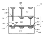
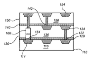
図1を参照すると、本発明の具体例にかかる半導体デバイス100の側面断面図が示されている。半導体デバイス100は、第1金属層110、第1誘電体層120、第2金属層130、第2誘電体層140および第3金属層150の順序で配列された積層構造を含んでもよい。更に、MTJデバイス160は、第1誘電体層120および第2金属層130の中に形成されまたは組み込まれ、第1金属層110および第3金属層150に電気的に接続されてもよい。MTJデバイス160は、例えば第1金属層110との境界面に配置された底部電極164を含む。
Referring to FIG. 1, a side cross-sectional view of a
第1金属層110は、誘電体材料116内に配置された金属配線114または導線を含んでもよい。誘電体材料116は、二酸化シリコンまたはlow−k材料の層などであってもよい。ある例では、金属配線114は、ダマシンプロセスによって形成され、そこでは誘電体材料116内のトレンチは、例えば銅などの金属で充填される。
The
第1誘電体層120は、第1金属層110と第2金属層130とを分離するように、例えば第1金属層110上に堆積されたSiCNの層を含んでもよい。図1に示されているように、第1誘電体層120は、第1金属層110の金属配線114の上に配置され、更に第2金属層130の中へ延びるMTJデバイス160を含んでもよい。
The
第1金属層110と同様に、第2金属層130は、low−k材料または超low−k材料などの誘電体材料136の層、および誘電体材料136のトレンチ内に形成された金属配線134を含んでもよい。第2金属層130の1つまたは複数の金属配線134は、第1誘電体層120に配置されたビア122によって、対応する第1金属層110の金属配線114に電気的に接続されてもよい。
Similar to the
第2誘電体層140は、第1誘電体層120と同様に構成されてもよく、したがって、第2金属層130上に堆積されたSiCNなどの層として形成されてもよい。続いて、第3金属層150は、low−k材料などの誘電体材料156の堆積によって、第2誘電体層140上に形成されてもよい。第3金属層150は、更に、第3金属層150の誘電体材料のトレンチ内に配置される金属配線154を含んでもよい。金属配線154のいくつかは、第2誘電体材料140内に配置されたビア接続部142によって、MTJデバイス160または第2金属層130の金属配線134に接続されてもよい。
The
このようにして、第1誘電体層120の最小の厚さが、MTJデバイス160(底部電極164を含む)の最大の高さに制限されない半導体デバイス100が提供される。図1に示されているように、前記第1誘電体層120および前記第2金属層130の厚さの合計hがMTJデバイスの高さを超える限り、MTJデバイス160は、第1誘電体層の厚さを超える高さを有してもよい。
In this way, the
図2は、本発明の具体例にかかるMTJデバイスの側面断面図を概略的に示している。MTJデバイスは、図1を参照して説明されたデバイスと同様に構成された半導体デバイスに組み込まれてもよい。MTJデバイス160は、磁気参照層またはピン層161、バリア層162および磁気自由層163などを有する複数の層のスタックを含んでもよい。磁気参照層161と自由層163の順序は、磁気参照層161がスタック内の磁気自由層163の上に配置されるように逆にされてもよいことに留意しなければならない。磁気参照層161および磁気自由層163は、例えば、磁気自由層163内の互いに反対の2つの方向の間で変更可能な方向を有する垂直磁気異方性を有してもよい。
FIG. 2 schematically shows a side sectional view of an MTJ device according to an embodiment of the invention. The MTJ device may be incorporated into a semiconductor device configured similar to the device described with reference to FIG. The
参照層161および自由層163は、CoFeBから形成され、または少なくともCoFeBを含んでもよい。CoFeBは、例えば、参照層161および/または自由層163の1つまたは複数の層に配置されてもよい。バリア層162は、MgOから形成され、または少なくともMgOを含み、電子が参照層161と自由層163の間をトンネルすることを可能にするように構成されてもよい。
The
図3a〜3eは、ある具体例にかかる製造プロセスの異なる段階における半導体デバイスの断面側面図を示している。得られる半導体デバイスは、図1および図2を参照して説明されたデバイスと同様に構成されてもよい。 3a-3e show cross-sectional side views of a semiconductor device at different stages of a manufacturing process according to an embodiment. The resulting semiconductor device may be configured similarly to the device described with reference to FIGS.
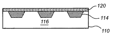
図3aは、例えばlow−k材料などの誘電体材料116を含む第1金属層110を示し、ここでトレンチは、エッチングされ、例えば銅114で充填されている。次に、オーバーバーデンは、CMPによって除去され、誘電体材料116に埋め込まれた露出した導電性の金属配線114を有する第1金属層110の平坦な表面が提供される。続いて、例えば25nmSiCNなどの誘電体材料の層が堆積され、第1誘電体層120を形成する。
FIG. 3 a shows a
図3bでは、MTJデバイス160は、第1金属層110の金属配線114の上に形成されている。MTJデバイス160は、例えば、(MTJデバイス160のための意図された位置にトレンチが設けられていて、下にある金属配線114を露出させる)第1誘電体層120の上にMTJデバイス160を形成する層のスタックを堆積させることによって形成されてもよい。底部電極164は、スタックの堆積の前に金属配線114の上に提供される。次に、堆積されたスタックは、ハードマスクによってエッチングされて、例えば第1誘電体層120の表面から突き出たピラーの形態のMTJデバイス160を規定する。次に、図3bに示されているように、第2金属層130の誘電体材料136が提供されて、MTJデバイス160の少なくとも一部が誘電体材料136の中に突き出る。
In FIG. 3 b, the
図3cでは、第2金属層130の誘電体材料136には、第1金属層110に関して説明したものと同様の方法でトレンチ内に配置された金属線134が提供されている。金属配線134は、例えばCMPプロセスによって規定されてもよく、MTJデバイス160が露出される前に、すなわちMTJデバイス160の上に誘電体材料136の少なくとも一部を残して、停止されてもよい。更に、電気的相互接続122またはビア接続が提供されて、第2金属層130と第1金属層110との間の接続を提供している。
In FIG. 3 c, the
次に、例えばSiCNなどの誘電体材料が堆積され、図3dに示されているように第2誘電体層140を形成してもよく、その上に例えばlow−k材料156の更なる層が堆積されて第3金属層150を形成してもよい。金属配線154は、第1金属層110および第2金属層130に関して説明されたものと同様の方法で、第3金属層150のトレンチ内に形成されてもよい。更に、ビア接続部142が形成されて、第3金属層150の金属配線154とMTJデバイス160との間の、および第3金属層150の金属配線154と第2金属層130の金属配線134との間の電気的な接続が提供されてもよい。
Next, a dielectric material such as SiCN may be deposited to form a
図4は、本発明の具体例にかかる半導体デバイスの製造方法を概略的に示している。半導体デバイスは、図1〜図3を参照して説明された半導体デバイスと同様に構成されてもよい。 FIG. 4 schematically shows a semiconductor device manufacturing method according to an embodiment of the present invention. The semiconductor device may be configured similarly to the semiconductor device described with reference to FIGS.
この方法は、第1金属層の上に第1誘電体層を形成するステップ410と、下層の第1金属層の金属配線を露出させるように第1誘電体層にビアトレンチを形成するステップ412とを含んでもよい。この方法は、更に、誘電体材料の層を堆積させるステップ422によって、第1誘電体層の上に第2金属層を形成するステップ420を含んでもよく、ここではMTJデバイスおよびメタルワイヤが形成されてもよい(430、432)。更に、第2誘電体層が形成され(440)、その上に第3金属層が提供されてもよい(450)。
The method includes forming 410 a first dielectric layer over the first metal layer and forming a via trench in the first dielectric layer so as to expose the metal wiring of the underlying
結論として、半導体デバイスおよびそのようなデバイスの製造方法が開示される。半導体デバイスは、MTJデバイスを含み、これは第1金属層および第3金属層に電気的に接続され、半導体デバイスの第1誘電体材料および第2金属層の中に組み込まれる。 In conclusion, semiconductor devices and methods of manufacturing such devices are disclosed. The semiconductor device includes an MTJ device, which is electrically connected to the first metal layer and the third metal layer and is incorporated into the first dielectric material and the second metal layer of the semiconductor device.
本発明は、添付の図面および前述の説明において詳細に図示され、説明されてきたが、そのような図示および説明は、説明的または例示的なものであり、制限的なものではないと考えられるべきである。本発明は、開示された具体例に限定されない。開示された具体例に対する他の変更は、図面、開示、および添付の特許請求の範囲の検討から、請求された発明を実施する当業者によって理解され、達成されることができる。特定の手段が相互に異なる従属請求項に列挙されているという単なる事実は、これらの手段の組み合わせが有利に使用できないことを示すものではない。特許請求の範囲内のいかなる参照符号も、その範囲を限定するものとして解釈されるべきではない。 While the invention has been illustrated and described in detail in the accompanying drawings and foregoing description, such illustration and description are to be considered illustrative or exemplary and not restrictive. Should. The invention is not limited to the disclosed embodiments. Other modifications to the disclosed embodiments can be understood and attained by those skilled in the art in practicing the claimed invention, from a study of the drawings, the disclosure, and the appended claims. The mere fact that certain measures are recited in mutually different dependent claims does not indicate that a combination of these measured cannot be used to advantage. Any reference signs in the claims should not be construed as limiting the scope.
Claims (14)
該第1金属層の上に配置された第1誘電体層と、
該第1誘電体層の上に配置された第2金属層と、
該第2金属層の上に配置された第2誘電体層と、
該第2誘電体層の上に配置された第3金属層と、
を含む半導体デバイスであって、
前記第1金属層は、前記第1誘電体層に配置されたビアによって前記第2金属層に電気的に接続され、
前記第2金属層は、前記第2誘電体層に配置されたビアによって前記第3金属層に電気的に接続され、
更に、該半導体デバイスは、前記第1誘電体層および前記第2金属層の中に配置され、前記第1金属層および前記第3金属層に電気的に接続され、高さが前記第1誘電体層の中のビアの長さを超えている磁気トンネル接合(MTJ)デバイスを含む半導体デバイス。 A first metal layer;
A first dielectric layer disposed on the first metal layer;
A second metal layer disposed on the first dielectric layer;
A second dielectric layer disposed on the second metal layer;
A third metal layer disposed on the second dielectric layer;
A semiconductor device comprising:
The first metal layer is electrically connected to the second metal layer by a via disposed in the first dielectric layer;
The second metal layer is electrically connected to the third metal layer by a via disposed in the second dielectric layer;
Further, the semiconductor device is disposed in the first dielectric layer and the second metal layer, and is electrically connected to the first metal layer and the third metal layer, and has a height of the first dielectric layer. A semiconductor device comprising a magnetic tunnel junction (MTJ) device that exceeds the length of a via in a body layer.
第1金属層の上に第1誘電体層を形成するステップと、
前記第1誘電体層の上に、前記第1誘電体層の中に配置されたビアによって前記第1金属層に電気的に接続された第2金属層を形成するステップと、
前記第1誘電体層および前記第1金属層の中に配置されたMTJデバイスを形成するステップと、
前記第2金属層の上に第2誘電体層を形成するステップと、
前記第2誘電体層の上に、前記第2誘電体層の中に配置されたビアによって前記第2金属層に電気的に接続された第3金属層を形成するステップと、
を含む製造方法。 A method of manufacturing a semiconductor device, comprising:
Forming a first dielectric layer on the first metal layer;
Forming a second metal layer on the first dielectric layer electrically connected to the first metal layer by a via disposed in the first dielectric layer;
Forming an MTJ device disposed in the first dielectric layer and the first metal layer;
Forming a second dielectric layer on the second metal layer;
Forming a third metal layer on the second dielectric layer electrically connected to the second metal layer by a via disposed in the second dielectric layer;
Manufacturing method.
前記ビアトレンチの中に、前記MTJデバイスを形成するスタックであって、前記第1誘電体層の厚さを超える高さを有する前記スタックを提供するステップと、
MTJデバイスのスタックを少なくとも部分的に囲むように配置された誘電体材料の層を提供するステップと、
前記誘電体材料の中に、第2金属層を形成するステップと、
を含む請求項10に記載の方法。 Forming a via trench in the first dielectric layer to expose the metal wiring of the underlying first metal layer;
Providing the stack in the via trench to form the MTJ device, the stack having a height that exceeds the thickness of the first dielectric layer;
Providing a layer of dielectric material disposed to at least partially surround the stack of MTJ devices;
Forming a second metal layer in the dielectric material;
The method of claim 10 comprising:
Applications Claiming Priority (2)
| Application Number | Priority Date | Filing Date | Title |
|---|---|---|---|
| EP15201487.4A EP3185321B1 (en) | 2015-12-21 | 2015-12-21 | Semiconductor device with integrated magnetic tunnel junction with a manufacturing method |
| EP15201487.4 | 2015-12-21 |
Publications (1)
| Publication Number | Publication Date |
|---|---|
| JP2017143247A true JP2017143247A (en) | 2017-08-17 |
Family
ID=55023957
Family Applications (1)
| Application Number | Title | Priority Date | Filing Date |
|---|---|---|---|
| JP2016246877A Pending JP2017143247A (en) | 2015-12-21 | 2016-12-20 | Semiconductor device with integrated magnetic tunnel junction |
Country Status (3)
| Country | Link |
|---|---|
| US (1) | US10170692B2 (en) |
| EP (1) | EP3185321B1 (en) |
| JP (1) | JP2017143247A (en) |
Families Citing this family (6)
| Publication number | Priority date | Publication date | Assignee | Title |
|---|---|---|---|---|
| US10008387B1 (en) | 2017-02-15 | 2018-06-26 | Globalfoundries Singapore Pte. Ltd. | Embedded memory in back-end-of-line low-k dielectric |
| US10347825B2 (en) * | 2017-02-17 | 2019-07-09 | International Business Machines Corporation | Selective deposition and nitridization of bottom electrode metal for MRAM applications |
| JP7367669B2 (en) | 2018-04-02 | 2023-10-24 | 株式会社ソシオネクスト | semiconductor equipment |
| US10622406B2 (en) * | 2018-07-03 | 2020-04-14 | International Business Machines Corporation | Dual metal nitride landing pad for MRAM devices |
| CN115377284A (en) * | 2021-05-18 | 2022-11-22 | 联华电子股份有限公司 | Semiconductor device with a plurality of semiconductor chips |
| US11910722B2 (en) | 2021-12-06 | 2024-02-20 | International Business Machines Corporation | Subtractive top via as a bottom electrode contact for an embedded memory |
Family Cites Families (7)
| Publication number | Priority date | Publication date | Assignee | Title |
|---|---|---|---|---|
| US7183130B2 (en) * | 2003-07-29 | 2007-02-27 | International Business Machines Corporation | Magnetic random access memory and method of fabricating thereof |
| US9159910B2 (en) * | 2008-04-21 | 2015-10-13 | Qualcomm Incorporated | One-mask MTJ integration for STT MRAM |
| JP5695453B2 (en) * | 2011-03-07 | 2015-04-08 | ルネサスエレクトロニクス株式会社 | Semiconductor device and manufacturing method of semiconductor device |
| US9741765B1 (en) * | 2012-08-14 | 2017-08-22 | Crossbar, Inc. | Monolithically integrated resistive memory using integrated-circuit foundry compatible processes |
| US8836056B2 (en) * | 2012-09-26 | 2014-09-16 | Intel Corporation | Perpendicular MTJ stacks with magnetic anisotropy enhancing layer and crystallization barrier layer |
| US9349772B2 (en) * | 2014-04-25 | 2016-05-24 | Globalfoundries Singapore Pte. Ltd. | Methods for fabricatingintegrated circuits with spin torque transfer magnetic randomaccess memory (STT-MRAM) including a passivation layer formed along lateral sidewalls of a magnetic tunnel junction of the STT-MRAM |
| US9412786B1 (en) * | 2014-10-02 | 2016-08-09 | Everspin Technologies, Inc. | Magnetoresistive device design and process integration with surrounding circuitry |
-
2015
- 2015-12-21 EP EP15201487.4A patent/EP3185321B1/en active Active
-
2016
- 2016-12-20 JP JP2016246877A patent/JP2017143247A/en active Pending
- 2016-12-21 US US15/387,127 patent/US10170692B2/en active Active
Also Published As
| Publication number | Publication date |
|---|---|
| US10170692B2 (en) | 2019-01-01 |
| US20170179378A1 (en) | 2017-06-22 |
| EP3185321B1 (en) | 2025-07-16 |
| EP3185321A1 (en) | 2017-06-28 |
Similar Documents
| Publication | Publication Date | Title |
|---|---|---|
| US12219880B2 (en) | Integrated circuit device | |
| JP5695453B2 (en) | Semiconductor device and manufacturing method of semiconductor device | |
| CN100444280C (en) | MRAM device and manufacturing method thereof | |
| CN105977376B (en) | Vertical magnetism tunnel knot for modified magnetic random access memory technique | |
| US9299745B2 (en) | Integrated circuits having magnetic tunnel junctions (MTJ) and methods for fabricating the same | |
| JP5690933B2 (en) | MRAM devices and integration techniques compatible with logic integrated circuits | |
| US6783999B1 (en) | Subtractive stud formation for MRAM manufacturing | |
| CN112447788B (en) | magnetoresistive random access memory | |
| US10008536B2 (en) | Encapsulation of magnetic tunnel junction structures in organic photopatternable dielectric material | |
| US10170692B2 (en) | Semiconductor device with integrated magnetic tunnel junction | |
| CN103354952B (en) | The MAGNETIC RANDOM ACCESS MEMORY of the size with improvement is integrated | |
| JP2006523963A (en) | Magnetoresistive random access memory device and manufacturing method thereof | |
| US10797224B2 (en) | Magnetoresistive device and method of fabricating same | |
| KR101159240B1 (en) | Method for fabricating semiconductor device | |
| JP2008518469A (en) | Magnetoresistive random access memory device structure and manufacturing method thereof | |
| TWI821466B (en) | Semiconductor device and method for fabricating the same | |
| CN109545744B (en) | A kind of magnetic random access memory cell array and manufacturing method of peripheral circuit connection | |
| JP2024531579A (en) | Magnetic tunnel junction devices with minimal stray magnetic fields | |
| JP2007165505A (en) | Semiconductor device and manufacturing method thereof | |
| TW202545301A (en) | Magnetoresistive random access memory device and manufacturing method thereof | |
| CN120835735A (en) | Magnetic storage bit, preparation method thereof and magnetic memory | |
| CN121240760A (en) | Spin-orbit torque magnetic random access memory device and its manufacturing method |