JP2017147343A - リソグラフィ装置および物品製造方法 - Google Patents
リソグラフィ装置および物品製造方法 Download PDFInfo
- Publication number
- JP2017147343A JP2017147343A JP2016028297A JP2016028297A JP2017147343A JP 2017147343 A JP2017147343 A JP 2017147343A JP 2016028297 A JP2016028297 A JP 2016028297A JP 2016028297 A JP2016028297 A JP 2016028297A JP 2017147343 A JP2017147343 A JP 2017147343A
- Authority
- JP
- Japan
- Prior art keywords
- lithographic apparatus
- substrate
- electrode
- electrode structure
- original plate
- Prior art date
- Legal status (The legal status is an assumption and is not a legal conclusion. Google has not performed a legal analysis and makes no representation as to the accuracy of the status listed.)
- Granted
Links
Images




Classifications
-
- G—PHYSICS
- G03—PHOTOGRAPHY; CINEMATOGRAPHY; ANALOGOUS TECHNIQUES USING WAVES OTHER THAN OPTICAL WAVES; ELECTROGRAPHY; HOLOGRAPHY
- G03F—PHOTOMECHANICAL PRODUCTION OF TEXTURED OR PATTERNED SURFACES, e.g. FOR PRINTING, FOR PROCESSING OF SEMICONDUCTOR DEVICES; MATERIALS THEREFOR; ORIGINALS THEREFOR; APPARATUS SPECIALLY ADAPTED THEREFOR
- G03F7/00—Photomechanical, e.g. photolithographic, production of textured or patterned surfaces, e.g. printing surfaces; Materials therefor, e.g. comprising photoresists; Apparatus specially adapted therefor
- G03F7/70—Microphotolithographic exposure; Apparatus therefor
- G03F7/70691—Handling of masks or workpieces
- G03F7/707—Chucks, e.g. chucking or un-chucking operations or structural details
- G03F7/70708—Chucks, e.g. chucking or un-chucking operations or structural details being electrostatic; Electrostatically deformable vacuum chucks
-
- G—PHYSICS
- G03—PHOTOGRAPHY; CINEMATOGRAPHY; ANALOGOUS TECHNIQUES USING WAVES OTHER THAN OPTICAL WAVES; ELECTROGRAPHY; HOLOGRAPHY
- G03F—PHOTOMECHANICAL PRODUCTION OF TEXTURED OR PATTERNED SURFACES, e.g. FOR PRINTING, FOR PROCESSING OF SEMICONDUCTOR DEVICES; MATERIALS THEREFOR; ORIGINALS THEREFOR; APPARATUS SPECIALLY ADAPTED THEREFOR
- G03F7/00—Photomechanical, e.g. photolithographic, production of textured or patterned surfaces, e.g. printing surfaces; Materials therefor, e.g. comprising photoresists; Apparatus specially adapted therefor
- G03F7/0002—Lithographic processes using patterning methods other than those involving the exposure to radiation, e.g. by stamping
-
- G—PHYSICS
- G03—PHOTOGRAPHY; CINEMATOGRAPHY; ANALOGOUS TECHNIQUES USING WAVES OTHER THAN OPTICAL WAVES; ELECTROGRAPHY; HOLOGRAPHY
- G03F—PHOTOMECHANICAL PRODUCTION OF TEXTURED OR PATTERNED SURFACES, e.g. FOR PRINTING, FOR PROCESSING OF SEMICONDUCTOR DEVICES; MATERIALS THEREFOR; ORIGINALS THEREFOR; APPARATUS SPECIALLY ADAPTED THEREFOR
- G03F7/00—Photomechanical, e.g. photolithographic, production of textured or patterned surfaces, e.g. printing surfaces; Materials therefor, e.g. comprising photoresists; Apparatus specially adapted therefor
- G03F7/70—Microphotolithographic exposure; Apparatus therefor
- G03F7/708—Construction of apparatus, e.g. environment aspects, hygiene aspects or materials
- G03F7/70908—Hygiene, e.g. preventing apparatus pollution, mitigating effect of pollution or removing pollutants from apparatus
-
- G—PHYSICS
- G03—PHOTOGRAPHY; CINEMATOGRAPHY; ANALOGOUS TECHNIQUES USING WAVES OTHER THAN OPTICAL WAVES; ELECTROGRAPHY; HOLOGRAPHY
- G03F—PHOTOMECHANICAL PRODUCTION OF TEXTURED OR PATTERNED SURFACES, e.g. FOR PRINTING, FOR PROCESSING OF SEMICONDUCTOR DEVICES; MATERIALS THEREFOR; ORIGINALS THEREFOR; APPARATUS SPECIALLY ADAPTED THEREFOR
- G03F7/00—Photomechanical, e.g. photolithographic, production of textured or patterned surfaces, e.g. printing surfaces; Materials therefor, e.g. comprising photoresists; Apparatus specially adapted therefor
- G03F7/70—Microphotolithographic exposure; Apparatus therefor
- G03F7/708—Construction of apparatus, e.g. environment aspects, hygiene aspects or materials
- G03F7/70908—Hygiene, e.g. preventing apparatus pollution, mitigating effect of pollution or removing pollutants from apparatus
- G03F7/70925—Cleaning, i.e. actively freeing apparatus from pollutants, e.g. using plasma cleaning
-
- G—PHYSICS
- G03—PHOTOGRAPHY; CINEMATOGRAPHY; ANALOGOUS TECHNIQUES USING WAVES OTHER THAN OPTICAL WAVES; ELECTROGRAPHY; HOLOGRAPHY
- G03F—PHOTOMECHANICAL PRODUCTION OF TEXTURED OR PATTERNED SURFACES, e.g. FOR PRINTING, FOR PROCESSING OF SEMICONDUCTOR DEVICES; MATERIALS THEREFOR; ORIGINALS THEREFOR; APPARATUS SPECIALLY ADAPTED THEREFOR
- G03F7/00—Photomechanical, e.g. photolithographic, production of textured or patterned surfaces, e.g. printing surfaces; Materials therefor, e.g. comprising photoresists; Apparatus specially adapted therefor
- G03F7/70—Microphotolithographic exposure; Apparatus therefor
- G03F7/708—Construction of apparatus, e.g. environment aspects, hygiene aspects or materials
- G03F7/70991—Connection with other apparatus, e.g. multiple exposure stations, particular arrangement of exposure apparatus and pre-exposure and/or post-exposure apparatus; Shared apparatus, e.g. having shared radiation source, shared mask or workpiece stage, shared base-plate; Utilities, e.g. cable, pipe or wireless arrangements for data, power, fluids or vacuum
-
- H—ELECTRICITY
- H10—SEMICONDUCTOR DEVICES; ELECTRIC SOLID-STATE DEVICES NOT OTHERWISE PROVIDED FOR
- H10D—INORGANIC ELECTRIC SEMICONDUCTOR DEVICES
- H10D64/00—Electrodes of devices having potential barriers
- H10D64/01—Manufacture or treatment
- H10D64/013—Manufacture or treatment of electrodes having a conductor capacitively coupled to a semiconductor by an insulator
-
- H—ELECTRICITY
- H10—SEMICONDUCTOR DEVICES; ELECTRIC SOLID-STATE DEVICES NOT OTHERWISE PROVIDED FOR
- H10P—GENERIC PROCESSES OR APPARATUS FOR THE MANUFACTURE OR TREATMENT OF DEVICES COVERED BY CLASS H10
- H10P76/00—Manufacture or treatment of masks on semiconductor bodies, e.g. by lithography or photolithography
- H10P76/20—Manufacture or treatment of masks on semiconductor bodies, e.g. by lithography or photolithography of masks comprising organic materials
- H10P76/204—Manufacture or treatment of masks on semiconductor bodies, e.g. by lithography or photolithography of masks comprising organic materials of organic photoresist masks
- H10P76/2041—Photolithographic processes
Landscapes
- Physics & Mathematics (AREA)
- General Physics & Mathematics (AREA)
- Engineering & Computer Science (AREA)
- Epidemiology (AREA)
- Health & Medical Sciences (AREA)
- Public Health (AREA)
- Environmental & Geological Engineering (AREA)
- Atmospheric Sciences (AREA)
- Life Sciences & Earth Sciences (AREA)
- Plasma & Fusion (AREA)
- Computer Networks & Wireless Communication (AREA)
- Shaping Of Tube Ends By Bending Or Straightening (AREA)
- Exposure Of Semiconductors, Excluding Electron Or Ion Beam Exposure (AREA)
- Exposure And Positioning Against Photoresist Photosensitive Materials (AREA)
Abstract
Description
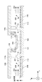
D=3√(νx/UU) (1)
で示される。ここで、U∞は主流の速度、νは気体の動粘度、xは周辺部材113の端からの距離である。電極構造140の複数の電極群における電極の配列ピッチPは、境界層厚Dより小さいことが好ましい。配列ピッチPは、隣り合う電極の中心間距離である。
ここで、CCはカニンガムの補正係数といわれる無次元数であり、パーティクル200の径と周囲の気体の平均自由工程のオーダーがほぼ同じになる場合に考慮すべき数である。ρPはパーティクル200の密度、Dpはパーティクル200の径、gは重力加速度である。
ここで、kはボルツマン係数、Tは気体の温度である。
ここで、pはパーティクルの荷電数である。インプリント装置IMPで発生するパーティクル200の荷電数は不明であるものの、ここでは、パーティクル200の径Dpに依存する平均の荷電数を仮定する。eは電気素量、Emaxは境界層内に発生させる電界強度の最大値である。
Claims (14)
- 原版のパターンを基板に転写するリソグラフィ装置であって、
前記基板および前記原版の一方の側面を取り囲むように配置された電極構造と、
前記電極構造に交流電圧を供給する電源と、を備え、
前記電極構造は、互いに電気的に絶縁された複数の電極群を含み、各電極群は、互いに電気的に接続された複数の電極を含み、
前記電源は、前記複数の電極群に対して互いに異なる位相を有する交流電圧を供給する、
ことを特徴とするリソグラフィ装置。 - 前記基板および前記原版の前記一方の側面を取り囲むように配置された周辺部材を更に備え、
前記周辺部材は、絶縁部材を含み、前記電極構造は、前記絶縁部材に埋め込まれている、
ことを特徴とする請求項1に記載のリソグラフィ装置。 - 前記周辺部材は、平坦な表面を有する、
ことを特徴とする請求項2に記載のリソグラフィ装置。 - 前記複数の電極群における電極の配列ピッチは、前記周辺部材の前記平坦な表面に対向しうる部材と前記表面との距離より小さい、
ことを特徴とする請求項3に記載のリソグラフィ装置。 - 前記電源が各電極群に供給する交流電圧の周波数は、1〜1000Hzの範囲内である、
ことを特徴とする請求項1乃至4のいずれか1項に記載のリソグラフィ装置。 - 前記基板と前記原版との間の空間に前記基板に沿った気体の流れが形成されるように、前記空間に向けて気体を供給する気体供給部を更に備える、
ことを特徴とする請求項1乃至5のいずれか1項に記載のリソグラフィ装置。 - 前記原版を取り囲むように配置され、気体を吹き出す吹き出し部を更に備える、
ことを特徴とする請求項6に記載のリソグラフィ装置。 - 前記基板および前記原版の他方の側面を取り囲むように配置された第2電極構造を更に備え、
前記第2電極構造は、互いに電気的に絶縁された複数の第2電極群を含み、各第2電極群は、互いに電気的に接続された複数の第2電極を含み、
前記電源は、前記複数の第2電極群に対して互いに異なる位相を有する交流電圧を供給する、
ことを特徴とする請求項1乃至7のいずれか1項に記載のリソグラフィ装置。 - 前記複数の電極群を構成する電極は、同心円状に配置されている、
ことを特徴とする請求項1乃至8のいずれか1項に記載のリソグラフィ装置。 - 前記複数の電極群を構成する各電極は、放射状に延びている、
ことを特徴とする請求項1乃至8のいずれか1項に記載のリソグラフィ装置。 - 前記複数の電極群によって電界の定在波が形成される、
ことを特徴とする請求項1乃至10のいずれか1項に記載のリソグラフィ装置。 - 前記複数の電極群によって電界の進行波が形成される、
ことを特徴とする請求項1乃至10のいずれか1項に記載のリソグラフィ装置。 - 前記進行波は、前記基板および前記原版の前記一方から離れる方向に進行するように形成される、
ことを特徴とするように形成される、
ことを特徴とする請求項12に記載のリソグラフィ装置。 - 請求項1乃至13のいずれか1項に記載のリソグラフィ装置を用いて基板の上にパターンを形成する工程と、
前記パターンが形成された前記基板を処理する工程と、
を含むことを特徴とする物品製造方法。
Priority Applications (6)
| Application Number | Priority Date | Filing Date | Title |
|---|---|---|---|
| JP2016028297A JP6643135B2 (ja) | 2016-02-17 | 2016-02-17 | リソグラフィ装置および物品製造方法 |
| SG10201700942WA SG10201700942WA (en) | 2016-02-17 | 2017-02-07 | Lithography apparatus and article manufacturing method |
| TW106104126A TWI663487B (zh) | 2016-02-17 | 2017-02-08 | 微影設備及物品製造方法 |
| US15/430,988 US10228624B2 (en) | 2016-02-17 | 2017-02-13 | Lithography apparatus and article manufacturing method |
| CN201710078450.6A CN107092163B (zh) | 2016-02-17 | 2017-02-14 | 光刻装置以及物品制造方法 |
| KR1020170020309A KR102091908B1 (ko) | 2016-02-17 | 2017-02-15 | 리소그래피 장치 및 물품 제조 방법 |
Applications Claiming Priority (1)
| Application Number | Priority Date | Filing Date | Title |
|---|---|---|---|
| JP2016028297A JP6643135B2 (ja) | 2016-02-17 | 2016-02-17 | リソグラフィ装置および物品製造方法 |
Publications (3)
| Publication Number | Publication Date |
|---|---|
| JP2017147343A true JP2017147343A (ja) | 2017-08-24 |
| JP2017147343A5 JP2017147343A5 (ja) | 2019-04-04 |
| JP6643135B2 JP6643135B2 (ja) | 2020-02-12 |
Family
ID=59561429
Family Applications (1)
| Application Number | Title | Priority Date | Filing Date |
|---|---|---|---|
| JP2016028297A Active JP6643135B2 (ja) | 2016-02-17 | 2016-02-17 | リソグラフィ装置および物品製造方法 |
Country Status (6)
| Country | Link |
|---|---|
| US (1) | US10228624B2 (ja) |
| JP (1) | JP6643135B2 (ja) |
| KR (1) | KR102091908B1 (ja) |
| CN (1) | CN107092163B (ja) |
| SG (1) | SG10201700942WA (ja) |
| TW (1) | TWI663487B (ja) |
Cited By (1)
| Publication number | Priority date | Publication date | Assignee | Title |
|---|---|---|---|---|
| JP2017157640A (ja) * | 2016-02-29 | 2017-09-07 | キヤノン株式会社 | インプリント装置、物品の製造方法、保持装置および露光装置 |
Families Citing this family (8)
| Publication number | Priority date | Publication date | Assignee | Title |
|---|---|---|---|---|
| US10722925B2 (en) * | 2017-12-04 | 2020-07-28 | Suss Micro Tec Photomask Equipment Gmbh & Co Kg | Treatment head, treatment system and method for treating a local surface area of a substrate |
| JP7348454B2 (ja) * | 2018-10-01 | 2023-09-21 | 東京エレクトロン株式会社 | 基板表面から異物を静電的に除去するための装置及び方法 |
| US11506985B2 (en) * | 2019-04-29 | 2022-11-22 | Taiwan Semiconductor Manufacturing Co., Ltd. | Semiconductor apparatus and method of operating the same for preventing photomask particulate contamination |
| JP7495814B2 (ja) * | 2020-05-13 | 2024-06-05 | キヤノン株式会社 | インプリント装置、および物品の製造方法 |
| WO2022159468A1 (en) * | 2021-01-20 | 2022-07-28 | Applied Materials, Inc. | Anti-slippery stamp landing ring |
| KR102542639B1 (ko) * | 2021-02-10 | 2023-06-12 | 성균관대학교산학협력단 | 미세 패턴 형성 장치 및 방법 |
| KR102528880B1 (ko) * | 2021-02-16 | 2023-05-03 | 성균관대학교산학협력단 | 전기수력학 불안정성을 이용한 패턴제작기술의 미세 구조체 사이의 2차 간섭효과에 의한 초미세구조체 제작 및 초소수성표면 형성방법 |
| US12463042B2 (en) | 2022-05-31 | 2025-11-04 | Canon Kabushiki Kaisha | Planarization system and method |
Citations (8)
| Publication number | Priority date | Publication date | Assignee | Title |
|---|---|---|---|---|
| JP2000228439A (ja) * | 1999-02-05 | 2000-08-15 | Advantest Corp | ステージ上のパーティクル除去方法及び清掃板 |
| JP2008258490A (ja) * | 2007-04-06 | 2008-10-23 | Canon Inc | 露光装置及び原版 |
| JP2009302234A (ja) * | 2008-06-12 | 2009-12-24 | Canon Inc | 露光装置及びデバイス製造方法 |
| JP2011040464A (ja) * | 2009-08-07 | 2011-02-24 | Canon Inc | 異物除去装置、露光装置及びデバイス製造方法 |
| US20130026393A1 (en) * | 2011-07-27 | 2013-01-31 | Gigaphoton Inc. | Chamber apparatus, extreme ultraviolet light generation system, and method for controlling the extreme ultraviolet light generation system |
| JP2013197465A (ja) * | 2012-03-22 | 2013-09-30 | Toshiba Corp | 静電チャック装置および露光装置 |
| JP2015149390A (ja) * | 2014-02-06 | 2015-08-20 | キヤノン株式会社 | インプリント装置、型、および物品の製造方法 |
| US20160236245A1 (en) * | 2015-02-12 | 2016-08-18 | Applied Materials, Inc. | Self-cleaning substrate contact surfaces |
Family Cites Families (8)
| Publication number | Priority date | Publication date | Assignee | Title |
|---|---|---|---|---|
| CN1222918C (zh) * | 2001-08-27 | 2005-10-12 | 佳能株式会社 | 布线基板及使用该布线基板的图象显示装置 |
| US8125603B2 (en) * | 2007-05-17 | 2012-02-28 | Lg Display Co., Ltd. | In-plane switching mode liquid crystal display device and method for fabricating the same |
| US7558045B1 (en) * | 2008-03-20 | 2009-07-07 | Novellus Systems, Inc. | Electrostatic chuck assembly with capacitive sense feature, and related operating method |
| JP2009246046A (ja) * | 2008-03-28 | 2009-10-22 | Canon Inc | 露光装置及びデバイス製造方法 |
| JP5828626B2 (ja) * | 2010-10-04 | 2015-12-09 | キヤノン株式会社 | インプリント方法 |
| DE102012017669A1 (de) * | 2012-09-07 | 2014-03-13 | Valeo Schalter Und Sensoren Gmbh | Anordnung mit einem Verkleidungsteil und einem Radarsensor, Kraftfahrzeug und Verfahren zum Herstellen einer Anordnung |
| TWI609763B (zh) | 2012-10-04 | 2018-01-01 | 大日本印刷股份有限公司 | 壓印方法及壓印裝置 |
| JP6171412B2 (ja) | 2013-03-06 | 2017-08-02 | 大日本印刷株式会社 | インプリント方法、インプリント用のモールドおよびインプリント装置 |
-
2016
- 2016-02-17 JP JP2016028297A patent/JP6643135B2/ja active Active
-
2017
- 2017-02-07 SG SG10201700942WA patent/SG10201700942WA/en unknown
- 2017-02-08 TW TW106104126A patent/TWI663487B/zh active
- 2017-02-13 US US15/430,988 patent/US10228624B2/en active Active
- 2017-02-14 CN CN201710078450.6A patent/CN107092163B/zh active Active
- 2017-02-15 KR KR1020170020309A patent/KR102091908B1/ko active Active
Patent Citations (8)
| Publication number | Priority date | Publication date | Assignee | Title |
|---|---|---|---|---|
| JP2000228439A (ja) * | 1999-02-05 | 2000-08-15 | Advantest Corp | ステージ上のパーティクル除去方法及び清掃板 |
| JP2008258490A (ja) * | 2007-04-06 | 2008-10-23 | Canon Inc | 露光装置及び原版 |
| JP2009302234A (ja) * | 2008-06-12 | 2009-12-24 | Canon Inc | 露光装置及びデバイス製造方法 |
| JP2011040464A (ja) * | 2009-08-07 | 2011-02-24 | Canon Inc | 異物除去装置、露光装置及びデバイス製造方法 |
| US20130026393A1 (en) * | 2011-07-27 | 2013-01-31 | Gigaphoton Inc. | Chamber apparatus, extreme ultraviolet light generation system, and method for controlling the extreme ultraviolet light generation system |
| JP2013197465A (ja) * | 2012-03-22 | 2013-09-30 | Toshiba Corp | 静電チャック装置および露光装置 |
| JP2015149390A (ja) * | 2014-02-06 | 2015-08-20 | キヤノン株式会社 | インプリント装置、型、および物品の製造方法 |
| US20160236245A1 (en) * | 2015-02-12 | 2016-08-18 | Applied Materials, Inc. | Self-cleaning substrate contact surfaces |
Non-Patent Citations (1)
| Title |
|---|
| C. I. CALLE, ET AL.: "Dust Particle removal by Electrostatic and Dielectrophoretic Forces with Applications to NASA Explor", PROC. ESA ANNUAL MEETING ON ELECTROSTATICS 2008, PAPER O1, JPN7019003899, 2008, pages 1 - 14, ISSN: 0004167135 * |
Cited By (1)
| Publication number | Priority date | Publication date | Assignee | Title |
|---|---|---|---|---|
| JP2017157640A (ja) * | 2016-02-29 | 2017-09-07 | キヤノン株式会社 | インプリント装置、物品の製造方法、保持装置および露光装置 |
Also Published As
| Publication number | Publication date |
|---|---|
| CN107092163A (zh) | 2017-08-25 |
| TW201740222A (zh) | 2017-11-16 |
| JP6643135B2 (ja) | 2020-02-12 |
| CN107092163B (zh) | 2020-12-29 |
| TWI663487B (zh) | 2019-06-21 |
| US10228624B2 (en) | 2019-03-12 |
| SG10201700942WA (en) | 2017-09-28 |
| US20170235234A1 (en) | 2017-08-17 |
| KR20170096961A (ko) | 2017-08-25 |
| KR102091908B1 (ko) | 2020-03-20 |
Similar Documents
| Publication | Publication Date | Title |
|---|---|---|
| JP6643135B2 (ja) | リソグラフィ装置および物品製造方法 | |
| US8226392B2 (en) | Transfer apparatus and method of manufacturing device | |
| KR102003630B1 (ko) | 임프린트 장치, 임프린트 방법, 및 물품 제조 방법 | |
| JP2015149390A (ja) | インプリント装置、型、および物品の製造方法 | |
| US10444646B2 (en) | Lithography apparatus and method of manufacturing article | |
| US11194249B2 (en) | Molding apparatus for molding composition on substrate with mold, and article manufacturing method | |
| WO2016170729A1 (en) | Imprint apparatus, method of imprinting, and method of manufacturing article | |
| JP2017139452A (ja) | インプリント装置および物品の製造方法 | |
| JP6789772B2 (ja) | インプリント装置、インプリント方法および物品製造方法 | |
| KR102206846B1 (ko) | 임프린트 장치 및 물품 제조 방법 | |
| US20250216310A1 (en) | Evaluation method, substrate processing apparatus, manufacturing method of substrate processing apparatus and article manufacturing method | |
| US10889052B2 (en) | Imprint apparatus, method for manufacturing article, and exposure apparatus | |
| JP2019067916A (ja) | リソグラフィ装置、および物品の製造方法 | |
| JP2017157641A (ja) | インプリント装置、インプリント方法、および物品の製造方法 | |
| JP7089420B2 (ja) | 基板処理装置、および物品製造方法 | |
| US20250201579A1 (en) | Planarization apparatus and article manufacturing method | |
| JP2021002626A (ja) | インプリント装置及び物品の製造方法 | |
| TW202608128A (zh) | 膜形成方法、膜形成裝置及物品製造方法 | |
| JP2025182613A (ja) | 膜形成方法、膜形成装置、および物品製造方法 | |
| JP2024051498A (ja) | 基板処理装置の評価方法 | |
| WO2017134989A1 (ja) | インプリント装置および物品の製造方法 | |
| JP2019117845A (ja) | リソグラフィ装置及び物品の製造方法 |
Legal Events
| Date | Code | Title | Description |
|---|---|---|---|
| A521 | Request for written amendment filed |
Free format text: JAPANESE INTERMEDIATE CODE: A523 Effective date: 20190218 |
|
| A621 | Written request for application examination |
Free format text: JAPANESE INTERMEDIATE CODE: A621 Effective date: 20190218 |
|
| TRDD | Decision of grant or rejection written | ||
| A977 | Report on retrieval |
Free format text: JAPANESE INTERMEDIATE CODE: A971007 Effective date: 20191127 |
|
| A01 | Written decision to grant a patent or to grant a registration (utility model) |
Free format text: JAPANESE INTERMEDIATE CODE: A01 Effective date: 20191206 |
|
| A61 | First payment of annual fees (during grant procedure) |
Free format text: JAPANESE INTERMEDIATE CODE: A61 Effective date: 20200106 |
|
| R151 | Written notification of patent or utility model registration |
Ref document number: 6643135 Country of ref document: JP Free format text: JAPANESE INTERMEDIATE CODE: R151 |