JP2017174855A - 基板保持装置および基板処理装置 - Google Patents
基板保持装置および基板処理装置 Download PDFInfo
- Publication number
- JP2017174855A JP2017174855A JP2016056007A JP2016056007A JP2017174855A JP 2017174855 A JP2017174855 A JP 2017174855A JP 2016056007 A JP2016056007 A JP 2016056007A JP 2016056007 A JP2016056007 A JP 2016056007A JP 2017174855 A JP2017174855 A JP 2017174855A
- Authority
- JP
- Japan
- Prior art keywords
- substrate
- negative pressure
- exhaust pipe
- holding
- holding device
- Prior art date
- Legal status (The legal status is an assumption and is not a legal conclusion. Google has not performed a legal analysis and makes no representation as to the accuracy of the status listed.)
- Granted
Links
Images



Classifications
-
- H—ELECTRICITY
- H10—SEMICONDUCTOR DEVICES; ELECTRIC SOLID-STATE DEVICES NOT OTHERWISE PROVIDED FOR
- H10P—GENERIC PROCESSES OR APPARATUS FOR THE MANUFACTURE OR TREATMENT OF DEVICES COVERED BY CLASS H10
- H10P72/00—Handling or holding of wafers, substrates or devices during manufacture or treatment thereof
- H10P72/10—Handling or holding of wafers, substrates or devices during manufacture or treatment thereof using carriers specially adapted therefor, e.g. front opening unified pods [FOUP]
- H10P72/17—Handling or holding of wafers, substrates or devices during manufacture or treatment thereof using carriers specially adapted therefor, e.g. front opening unified pods [FOUP] specially adapted for supporting large square shaped substrates
-
- G—PHYSICS
- G03—PHOTOGRAPHY; CINEMATOGRAPHY; ANALOGOUS TECHNIQUES USING WAVES OTHER THAN OPTICAL WAVES; ELECTROGRAPHY; HOLOGRAPHY
- G03F—PHOTOMECHANICAL PRODUCTION OF TEXTURED OR PATTERNED SURFACES, e.g. FOR PRINTING, FOR PROCESSING OF SEMICONDUCTOR DEVICES; MATERIALS THEREFOR; ORIGINALS THEREFOR; APPARATUS SPECIALLY ADAPTED THEREFOR
- G03F1/00—Originals for photomechanical production of textured or patterned surfaces, e.g., masks, photo-masks, reticles; Mask blanks or pellicles therefor; Containers specially adapted therefor; Preparation thereof
- G03F1/38—Masks having auxiliary features, e.g. special coatings or marks for alignment or testing; Preparation thereof
- G03F1/48—Protective coatings
-
- G—PHYSICS
- G03—PHOTOGRAPHY; CINEMATOGRAPHY; ANALOGOUS TECHNIQUES USING WAVES OTHER THAN OPTICAL WAVES; ELECTROGRAPHY; HOLOGRAPHY
- G03F—PHOTOMECHANICAL PRODUCTION OF TEXTURED OR PATTERNED SURFACES, e.g. FOR PRINTING, FOR PROCESSING OF SEMICONDUCTOR DEVICES; MATERIALS THEREFOR; ORIGINALS THEREFOR; APPARATUS SPECIALLY ADAPTED THEREFOR
- G03F7/00—Photomechanical, e.g. photolithographic, production of textured or patterned surfaces, e.g. printing surfaces; Materials therefor, e.g. comprising photoresists; Apparatus specially adapted therefor
- G03F7/002—Photomechanical, e.g. photolithographic, production of textured or patterned surfaces, e.g. printing surfaces; Materials therefor, e.g. comprising photoresists; Apparatus specially adapted therefor using materials containing microcapsules; Preparing or processing such materials, e.g. by pressure; Devices or apparatus specially designed therefor
- G03F7/0022—Devices or apparatus
- G03F7/0025—Devices or apparatus characterised by means for coating the developer
-
- G—PHYSICS
- G03—PHOTOGRAPHY; CINEMATOGRAPHY; ANALOGOUS TECHNIQUES USING WAVES OTHER THAN OPTICAL WAVES; ELECTROGRAPHY; HOLOGRAPHY
- G03F—PHOTOMECHANICAL PRODUCTION OF TEXTURED OR PATTERNED SURFACES, e.g. FOR PRINTING, FOR PROCESSING OF SEMICONDUCTOR DEVICES; MATERIALS THEREFOR; ORIGINALS THEREFOR; APPARATUS SPECIALLY ADAPTED THEREFOR
- G03F7/00—Photomechanical, e.g. photolithographic, production of textured or patterned surfaces, e.g. printing surfaces; Materials therefor, e.g. comprising photoresists; Apparatus specially adapted therefor
- G03F7/16—Coating processes; Apparatus therefor
-
- H—ELECTRICITY
- H10—SEMICONDUCTOR DEVICES; ELECTRIC SOLID-STATE DEVICES NOT OTHERWISE PROVIDED FOR
- H10P—GENERIC PROCESSES OR APPARATUS FOR THE MANUFACTURE OR TREATMENT OF DEVICES COVERED BY CLASS H10
- H10P14/00—Formation of materials, e.g. in the shape of layers or pillars
- H10P14/60—Formation of materials, e.g. in the shape of layers or pillars of insulating materials
- H10P14/65—Formation of materials, e.g. in the shape of layers or pillars of insulating materials characterised by treatments performed before or after the formation of the materials
- H10P14/6502—Formation of materials, e.g. in the shape of layers or pillars of insulating materials characterised by treatments performed before or after the formation of the materials of treatments performed before formation of the materials
- H10P14/6508—Formation of materials, e.g. in the shape of layers or pillars of insulating materials characterised by treatments performed before or after the formation of the materials of treatments performed before formation of the materials by exposure to a liquid
-
- H—ELECTRICITY
- H10—SEMICONDUCTOR DEVICES; ELECTRIC SOLID-STATE DEVICES NOT OTHERWISE PROVIDED FOR
- H10P—GENERIC PROCESSES OR APPARATUS FOR THE MANUFACTURE OR TREATMENT OF DEVICES COVERED BY CLASS H10
- H10P14/00—Formation of materials, e.g. in the shape of layers or pillars
- H10P14/60—Formation of materials, e.g. in the shape of layers or pillars of insulating materials
- H10P14/65—Formation of materials, e.g. in the shape of layers or pillars of insulating materials characterised by treatments performed before or after the formation of the materials
- H10P14/6516—Formation of materials, e.g. in the shape of layers or pillars of insulating materials characterised by treatments performed before or after the formation of the materials of treatments performed after formation of the materials
- H10P14/6534—Formation of materials, e.g. in the shape of layers or pillars of insulating materials characterised by treatments performed before or after the formation of the materials of treatments performed after formation of the materials by exposure to a liquid
-
- H—ELECTRICITY
- H10—SEMICONDUCTOR DEVICES; ELECTRIC SOLID-STATE DEVICES NOT OTHERWISE PROVIDED FOR
- H10P—GENERIC PROCESSES OR APPARATUS FOR THE MANUFACTURE OR TREATMENT OF DEVICES COVERED BY CLASS H10
- H10P72/00—Handling or holding of wafers, substrates or devices during manufacture or treatment thereof
- H10P72/70—Handling or holding of wafers, substrates or devices during manufacture or treatment thereof for supporting or gripping
- H10P72/74—Handling or holding of wafers, substrates or devices during manufacture or treatment thereof for supporting or gripping using temporarily an auxiliary support
-
- H—ELECTRICITY
- H10—SEMICONDUCTOR DEVICES; ELECTRIC SOLID-STATE DEVICES NOT OTHERWISE PROVIDED FOR
- H10P—GENERIC PROCESSES OR APPARATUS FOR THE MANUFACTURE OR TREATMENT OF DEVICES COVERED BY CLASS H10
- H10P72/00—Handling or holding of wafers, substrates or devices during manufacture or treatment thereof
- H10P72/70—Handling or holding of wafers, substrates or devices during manufacture or treatment thereof for supporting or gripping
- H10P72/76—Handling or holding of wafers, substrates or devices during manufacture or treatment thereof for supporting or gripping using mechanical means, e.g. clamps or pinches
- H10P72/7604—Handling or holding of wafers, substrates or devices during manufacture or treatment thereof for supporting or gripping using mechanical means, e.g. clamps or pinches the wafers being placed on a susceptor, stage or support
- H10P72/7612—Handling or holding of wafers, substrates or devices during manufacture or treatment thereof for supporting or gripping using mechanical means, e.g. clamps or pinches the wafers being placed on a susceptor, stage or support characterised by lifting arrangements, e.g. lift pins
-
- H—ELECTRICITY
- H10—SEMICONDUCTOR DEVICES; ELECTRIC SOLID-STATE DEVICES NOT OTHERWISE PROVIDED FOR
- H10P—GENERIC PROCESSES OR APPARATUS FOR THE MANUFACTURE OR TREATMENT OF DEVICES COVERED BY CLASS H10
- H10P72/00—Handling or holding of wafers, substrates or devices during manufacture or treatment thereof
- H10P72/70—Handling or holding of wafers, substrates or devices during manufacture or treatment thereof for supporting or gripping
- H10P72/78—Handling or holding of wafers, substrates or devices during manufacture or treatment thereof for supporting or gripping using vacuum or suction, e.g. Bernoulli chucks
Landscapes
- Physics & Mathematics (AREA)
- General Physics & Mathematics (AREA)
- Container, Conveyance, Adherence, Positioning, Of Wafer (AREA)
Abstract
Description
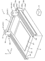
2 スリットノズル
3 基板
4 ステージ(保持部)
5 塗布処理部(処理部)
6 制御部
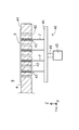
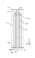
7 リフトピン
9 基板保持装置
40 昇降部
41 保持面
42 吸着孔
43 ピン孔
45 昇降駆動部
54 リニアモータ
71 シール部材
71a 切欠き部
80 配管系
81 第1排気配管
82 第2排気配管
83 第1切換えバルブ
84 第2切換えバルブ
85 負圧源
86 圧空源
87 圧空配管
88 開放配管
Claims (8)
- 基板が載置される保持面を有する保持部と、
保持部に設けられた複数の吸着孔と、
保持面に対して昇降する複数のリフトピンと、
保持部に設けられ、複数のリフトピンがそれぞれ挿通される複数のピン孔と、
複数の吸引孔に負圧を発生させる第1負圧発生部と、
複数のピン孔の内、1以上のピン孔に負圧を発生される第2負圧発生部と、
を備える基板保持装置。 - 請求項1に記載される基板保持装置において、
リフトピンが挿通されるとともに、ピン孔内にて上方空間と下方空間との間をシールするシール部材と、
シール部材に設けられた切欠き部と、
をさらに備え、
前記切欠き部により排気流路が形成される基板保持装置。 - 請求項1または請求項2に記載される基板保持装置において、
第1負圧発生部は、
複数の吸着孔と負圧源とを流路接続する第1排気配管と、
第1排気配管と圧空源とを流路接続する圧空配管と、
第1排気配管が負圧源に流路接続する吸着状態、または、第1排気配管が圧空配管に流路接続する吸着解除状態に選択的に切り替える第1切換えバルブと、を有し、
第2負圧発生部は、
ピン孔と負圧源とを流路接続する第2排気配管と、
第2排気配管を大気に開放する開放配管と、
第2排気配管が負圧源に流路接続する吸着状態、または、第2排気配管が開放配管に流路接続する吸着解除状態に選択的に切り替える第2切換えバルブと、を有する基板保持装置。 - 請求項1から請求項3のいずれに記載される基板保持装置において、
第2負圧発生部は複数のピン孔の内の一部のピン孔についてのみに負圧を発生させる基板保持装置。 - 請求項4に記載される基板保持装置において、
第2負圧発生部は複数のピン孔の内の保持面に載置される基板の中央部に対向するピン孔についてのみに負圧を発生させる基板保持装置。 - 請求項1から請求項5のいずれかに記載される基板保持装置と、
基板保持装置の保持部に保持された基板に所定の処理を施す処理部と、
を備える基板処理装置。 - 請求項6に記載される基板処理装置において、
処理部が基板保持装置の保持部に保持された基板の表面に塗布液を塗布する塗布処理部である基板処理装置。 - 請求項7に記載される基板処理装置において、
塗布処理部がスリット状の吐出口から塗布液を吐出するスリットノズルと、吐出口の長手方向と直交する方向にスリットノズルを移動させるスリットノズル移動部とを有する基板処理装置。
Priority Applications (3)
| Application Number | Priority Date | Filing Date | Title |
|---|---|---|---|
| JP2016056007A JP6596371B2 (ja) | 2016-03-18 | 2016-03-18 | 基板保持装置および基板処理装置 |
| TW105142836A TWI625817B (zh) | 2016-03-18 | 2016-12-23 | 基板保持裝置及基板處理裝置 |
| KR1020170015616A KR101946701B1 (ko) | 2016-03-18 | 2017-02-03 | 기판 유지 장치 및 기판 처리 장치 |
Applications Claiming Priority (1)
| Application Number | Priority Date | Filing Date | Title |
|---|---|---|---|
| JP2016056007A JP6596371B2 (ja) | 2016-03-18 | 2016-03-18 | 基板保持装置および基板処理装置 |
Publications (2)
| Publication Number | Publication Date |
|---|---|
| JP2017174855A true JP2017174855A (ja) | 2017-09-28 |
| JP6596371B2 JP6596371B2 (ja) | 2019-10-23 |
Family
ID=59972207
Family Applications (1)
| Application Number | Title | Priority Date | Filing Date |
|---|---|---|---|
| JP2016056007A Active JP6596371B2 (ja) | 2016-03-18 | 2016-03-18 | 基板保持装置および基板処理装置 |
Country Status (3)
| Country | Link |
|---|---|
| JP (1) | JP6596371B2 (ja) |
| KR (1) | KR101946701B1 (ja) |
| TW (1) | TWI625817B (ja) |
Cited By (3)
| Publication number | Priority date | Publication date | Assignee | Title |
|---|---|---|---|---|
| JP2019220851A (ja) * | 2018-06-20 | 2019-12-26 | キヤノン株式会社 | 電子機器 |
| WO2023114410A1 (en) * | 2021-12-16 | 2023-06-22 | Applied Materials, Inc. | Substrate support gap pumping to prevent glow discharge and light-up |
| CN116774526A (zh) * | 2023-05-09 | 2023-09-19 | 合肥芯碁微电子装备股份有限公司 | 一种直写曝光机的吸盘系统 |
Families Citing this family (1)
| Publication number | Priority date | Publication date | Assignee | Title |
|---|---|---|---|---|
| JP7812243B2 (ja) * | 2022-02-21 | 2026-02-09 | 株式会社Screenホールディングス | 基板保持装置および基板処理システム |
Citations (4)
| Publication number | Priority date | Publication date | Assignee | Title |
|---|---|---|---|---|
| JPH0786247A (ja) * | 1993-09-16 | 1995-03-31 | Hitachi Ltd | 減圧雰囲気内における被処理物の処理方法及び処理装置 |
| JP2007258439A (ja) * | 2006-03-23 | 2007-10-04 | Dainippon Screen Mfg Co Ltd | 熱処理プレート |
| JP2008098575A (ja) * | 2006-10-16 | 2008-04-24 | Ntn Corp | チャックステージおよびそれを用いたパターン修正装置 |
| JP2012186429A (ja) * | 2011-03-08 | 2012-09-27 | Mitsubishi Electric Corp | 基板処理装置と該基板処理装置を用いた基板処理方法 |
Family Cites Families (5)
| Publication number | Priority date | Publication date | Assignee | Title |
|---|---|---|---|---|
| JP2000100895A (ja) * | 1998-09-18 | 2000-04-07 | Nikon Corp | 基板の搬送装置、基板の保持装置、及び基板処理装置 |
| JP4410063B2 (ja) * | 2004-09-06 | 2010-02-03 | 東京エレクトロン株式会社 | 基板処理装置 |
| JP4707593B2 (ja) * | 2006-03-23 | 2011-06-22 | 大日本スクリーン製造株式会社 | 熱処理装置と基板吸着方法 |
| JP4712614B2 (ja) | 2006-05-29 | 2011-06-29 | 株式会社アルバック | 真空処理装置 |
| KR101494924B1 (ko) * | 2009-10-16 | 2015-02-23 | 도쿄엘렉트론가부시키가이샤 | 감압건조장치 및 감압건조방법 |
-
2016
- 2016-03-18 JP JP2016056007A patent/JP6596371B2/ja active Active
- 2016-12-23 TW TW105142836A patent/TWI625817B/zh active
-
2017
- 2017-02-03 KR KR1020170015616A patent/KR101946701B1/ko active Active
Patent Citations (4)
| Publication number | Priority date | Publication date | Assignee | Title |
|---|---|---|---|---|
| JPH0786247A (ja) * | 1993-09-16 | 1995-03-31 | Hitachi Ltd | 減圧雰囲気内における被処理物の処理方法及び処理装置 |
| JP2007258439A (ja) * | 2006-03-23 | 2007-10-04 | Dainippon Screen Mfg Co Ltd | 熱処理プレート |
| JP2008098575A (ja) * | 2006-10-16 | 2008-04-24 | Ntn Corp | チャックステージおよびそれを用いたパターン修正装置 |
| JP2012186429A (ja) * | 2011-03-08 | 2012-09-27 | Mitsubishi Electric Corp | 基板処理装置と該基板処理装置を用いた基板処理方法 |
Cited By (7)
| Publication number | Priority date | Publication date | Assignee | Title |
|---|---|---|---|---|
| JP2019220851A (ja) * | 2018-06-20 | 2019-12-26 | キヤノン株式会社 | 電子機器 |
| JP7130457B2 (ja) | 2018-06-20 | 2022-09-05 | キヤノン株式会社 | 電子機器 |
| WO2023114410A1 (en) * | 2021-12-16 | 2023-06-22 | Applied Materials, Inc. | Substrate support gap pumping to prevent glow discharge and light-up |
| JP2024546133A (ja) * | 2021-12-16 | 2024-12-17 | アプライド マテリアルズ インコーポレイテッド | グロー放電と点灯を防止するための基板支持体の間隙ポンピング |
| US12334383B2 (en) | 2021-12-16 | 2025-06-17 | Applied Materials, Inc. | Substrate support gap pumping to prevent glow discharge and light-up |
| JP7835861B2 (ja) | 2021-12-16 | 2026-03-25 | アプライド マテリアルズ インコーポレイテッド | グロー放電と点灯を防止するための基板支持体の間隙ポンピング |
| CN116774526A (zh) * | 2023-05-09 | 2023-09-19 | 合肥芯碁微电子装备股份有限公司 | 一种直写曝光机的吸盘系统 |
Also Published As
| Publication number | Publication date |
|---|---|
| KR20170108807A (ko) | 2017-09-27 |
| TWI625817B (zh) | 2018-06-01 |
| KR101946701B1 (ko) | 2019-02-11 |
| TW201735228A (zh) | 2017-10-01 |
| JP6596371B2 (ja) | 2019-10-23 |
Similar Documents
| Publication | Publication Date | Title |
|---|---|---|
| CN1328780C (zh) | 基板处理装置及基板处理方法 | |
| JP6407803B2 (ja) | 接合装置、接合システム、接合方法、プログラム及びコンピュータ記憶媒体 | |
| JP6596371B2 (ja) | 基板保持装置および基板処理装置 | |
| CN113262951B (zh) | 基板处理装置及基板处理方法 | |
| TWI593617B (zh) | 剝離裝置 | |
| KR20170048787A (ko) | 기판 처리 장치 및 기판 처리 방법 | |
| JP2009004545A (ja) | 基板載置装置および基板処理装置 | |
| JP3597321B2 (ja) | 減圧乾燥装置 | |
| TW201347078A (zh) | 基板處理裝置及基板處理方法 | |
| JP5720201B2 (ja) | ワーク移載装置 | |
| JP2011086875A (ja) | 塗布装置 | |
| JP2009032915A (ja) | 基板保持装置 | |
| KR101344926B1 (ko) | 지지유닛, 이를 포함하는 기판처리장치 | |
| JP6855334B2 (ja) | 基板処理装置及び基板処理方法 | |
| JP6595276B2 (ja) | 基板処理装置および基板処理方法 | |
| KR20110081494A (ko) | 기판 이송 장치 | |
| KR101468664B1 (ko) | 인쇄회로기판용 노광장치의 기판흡착장치 | |
| CN1812073A (zh) | 定位装置 | |
| KR20170056224A (ko) | 베이크 장치 및 베이크 방법 | |
| JP2015195276A (ja) | 基板処理装置および基板処理システム | |
| JP4758326B2 (ja) | 塗布装置 | |
| JP2025127534A (ja) | 基板保持装置、基板処理装置および基板保持方法 | |
| JP2014148386A (ja) | 基材搬送装置 | |
| CN206293422U (zh) | 基板保持装置及基板处理装置 | |
| WO2023120145A1 (ja) | 塗布装置及び塗布方法 |
Legal Events
| Date | Code | Title | Description |
|---|---|---|---|
| RD03 | Notification of appointment of power of attorney |
Free format text: JAPANESE INTERMEDIATE CODE: A7423 Effective date: 20160905 |
|
| RD04 | Notification of resignation of power of attorney |
Free format text: JAPANESE INTERMEDIATE CODE: A7424 Effective date: 20170725 |
|
| A621 | Written request for application examination |
Free format text: JAPANESE INTERMEDIATE CODE: A621 Effective date: 20181221 |
|
| A977 | Report on retrieval |
Free format text: JAPANESE INTERMEDIATE CODE: A971007 Effective date: 20190906 |
|
| TRDD | Decision of grant or rejection written | ||
| A01 | Written decision to grant a patent or to grant a registration (utility model) |
Free format text: JAPANESE INTERMEDIATE CODE: A01 Effective date: 20190917 |
|
| A61 | First payment of annual fees (during grant procedure) |
Free format text: JAPANESE INTERMEDIATE CODE: A61 Effective date: 20190930 |
|
| R150 | Certificate of patent or registration of utility model |
Ref document number: 6596371 Country of ref document: JP Free format text: JAPANESE INTERMEDIATE CODE: R150 |
|
| R250 | Receipt of annual fees |
Free format text: JAPANESE INTERMEDIATE CODE: R250 |
|
| R250 | Receipt of annual fees |
Free format text: JAPANESE INTERMEDIATE CODE: R250 |
|
| R250 | Receipt of annual fees |
Free format text: JAPANESE INTERMEDIATE CODE: R250 |
|
| R250 | Receipt of annual fees |
Free format text: JAPANESE INTERMEDIATE CODE: R250 |