JP2017183310A - 液処理装置 - Google Patents
液処理装置 Download PDFInfo
- Publication number
- JP2017183310A JP2017183310A JP2016063210A JP2016063210A JP2017183310A JP 2017183310 A JP2017183310 A JP 2017183310A JP 2016063210 A JP2016063210 A JP 2016063210A JP 2016063210 A JP2016063210 A JP 2016063210A JP 2017183310 A JP2017183310 A JP 2017183310A
- Authority
- JP
- Japan
- Prior art keywords
- substrate
- wafer
- support members
- processing apparatus
- liquid processing
- Prior art date
- Legal status (The legal status is an assumption and is not a legal conclusion. Google has not performed a legal analysis and makes no representation as to the accuracy of the status listed.)
- Granted
Links
Images






Classifications
-
- H—ELECTRICITY
- H10—SEMICONDUCTOR DEVICES; ELECTRIC SOLID-STATE DEVICES NOT OTHERWISE PROVIDED FOR
- H10P—GENERIC PROCESSES OR APPARATUS FOR THE MANUFACTURE OR TREATMENT OF DEVICES COVERED BY CLASS H10
- H10P72/00—Handling or holding of wafers, substrates or devices during manufacture or treatment thereof
- H10P72/04—Apparatus for manufacture or treatment
- H10P72/0402—Apparatus for fluid treatment
-
- H—ELECTRICITY
- H10—SEMICONDUCTOR DEVICES; ELECTRIC SOLID-STATE DEVICES NOT OTHERWISE PROVIDED FOR
- H10P—GENERIC PROCESSES OR APPARATUS FOR THE MANUFACTURE OR TREATMENT OF DEVICES COVERED BY CLASS H10
- H10P72/00—Handling or holding of wafers, substrates or devices during manufacture or treatment thereof
- H10P72/04—Apparatus for manufacture or treatment
- H10P72/0402—Apparatus for fluid treatment
- H10P72/0406—Apparatus for fluid treatment for cleaning followed by drying, rinsing, stripping, blasting or the like
- H10P72/0411—Apparatus for fluid treatment for cleaning followed by drying, rinsing, stripping, blasting or the like for wet cleaning or washing
- H10P72/0412—Apparatus for fluid treatment for cleaning followed by drying, rinsing, stripping, blasting or the like for wet cleaning or washing using mainly scrubbing means, e.g. brushes
-
- H—ELECTRICITY
- H10—SEMICONDUCTOR DEVICES; ELECTRIC SOLID-STATE DEVICES NOT OTHERWISE PROVIDED FOR
- H10P—GENERIC PROCESSES OR APPARATUS FOR THE MANUFACTURE OR TREATMENT OF DEVICES COVERED BY CLASS H10
- H10P70/00—Cleaning of wafers, substrates or parts of devices
- H10P70/10—Cleaning before device manufacture, i.e. Begin-Of-Line process
- H10P70/15—Cleaning before device manufacture, i.e. Begin-Of-Line process by wet cleaning only
-
- B—PERFORMING OPERATIONS; TRANSPORTING
- B08—CLEANING
- B08B—CLEANING IN GENERAL; PREVENTION OF FOULING IN GENERAL
- B08B1/00—Cleaning by methods involving the use of tools
- B08B1/10—Cleaning by methods involving the use of tools characterised by the type of cleaning tool
- B08B1/12—Brushes
-
- B—PERFORMING OPERATIONS; TRANSPORTING
- B08—CLEANING
- B08B—CLEANING IN GENERAL; PREVENTION OF FOULING IN GENERAL
- B08B17/00—Methods preventing fouling
-
- H—ELECTRICITY
- H10—SEMICONDUCTOR DEVICES; ELECTRIC SOLID-STATE DEVICES NOT OTHERWISE PROVIDED FOR
- H10P—GENERIC PROCESSES OR APPARATUS FOR THE MANUFACTURE OR TREATMENT OF DEVICES COVERED BY CLASS H10
- H10P70/00—Cleaning of wafers, substrates or parts of devices
- H10P70/60—Cleaning only by mechanical processes
-
- H—ELECTRICITY
- H10—SEMICONDUCTOR DEVICES; ELECTRIC SOLID-STATE DEVICES NOT OTHERWISE PROVIDED FOR
- H10P—GENERIC PROCESSES OR APPARATUS FOR THE MANUFACTURE OR TREATMENT OF DEVICES COVERED BY CLASS H10
- H10P72/00—Handling or holding of wafers, substrates or devices during manufacture or treatment thereof
- H10P72/04—Apparatus for manufacture or treatment
- H10P72/0402—Apparatus for fluid treatment
- H10P72/0404—Apparatus for fluid treatment for general liquid treatment, e.g. etching followed by cleaning
-
- H—ELECTRICITY
- H10—SEMICONDUCTOR DEVICES; ELECTRIC SOLID-STATE DEVICES NOT OTHERWISE PROVIDED FOR
- H10P—GENERIC PROCESSES OR APPARATUS FOR THE MANUFACTURE OR TREATMENT OF DEVICES COVERED BY CLASS H10
- H10P72/00—Handling or holding of wafers, substrates or devices during manufacture or treatment thereof
- H10P72/04—Apparatus for manufacture or treatment
- H10P72/0402—Apparatus for fluid treatment
- H10P72/0406—Apparatus for fluid treatment for cleaning followed by drying, rinsing, stripping, blasting or the like
- H10P72/0411—Apparatus for fluid treatment for cleaning followed by drying, rinsing, stripping, blasting or the like for wet cleaning or washing
- H10P72/0414—Apparatus for fluid treatment for cleaning followed by drying, rinsing, stripping, blasting or the like for wet cleaning or washing using mainly spraying means, e.g. nozzles
-
- H—ELECTRICITY
- H10—SEMICONDUCTOR DEVICES; ELECTRIC SOLID-STATE DEVICES NOT OTHERWISE PROVIDED FOR
- H10P—GENERIC PROCESSES OR APPARATUS FOR THE MANUFACTURE OR TREATMENT OF DEVICES COVERED BY CLASS H10
- H10P72/00—Handling or holding of wafers, substrates or devices during manufacture or treatment thereof
- H10P72/70—Handling or holding of wafers, substrates or devices during manufacture or treatment thereof for supporting or gripping
-
- H—ELECTRICITY
- H10—SEMICONDUCTOR DEVICES; ELECTRIC SOLID-STATE DEVICES NOT OTHERWISE PROVIDED FOR
- H10P—GENERIC PROCESSES OR APPARATUS FOR THE MANUFACTURE OR TREATMENT OF DEVICES COVERED BY CLASS H10
- H10P72/00—Handling or holding of wafers, substrates or devices during manufacture or treatment thereof
- H10P72/70—Handling or holding of wafers, substrates or devices during manufacture or treatment thereof for supporting or gripping
- H10P72/76—Handling or holding of wafers, substrates or devices during manufacture or treatment thereof for supporting or gripping using mechanical means, e.g. clamps or pinches
- H10P72/7604—Handling or holding of wafers, substrates or devices during manufacture or treatment thereof for supporting or gripping using mechanical means, e.g. clamps or pinches the wafers being placed on a susceptor, stage or support
-
- H—ELECTRICITY
- H10—SEMICONDUCTOR DEVICES; ELECTRIC SOLID-STATE DEVICES NOT OTHERWISE PROVIDED FOR
- H10P—GENERIC PROCESSES OR APPARATUS FOR THE MANUFACTURE OR TREATMENT OF DEVICES COVERED BY CLASS H10
- H10P72/00—Handling or holding of wafers, substrates or devices during manufacture or treatment thereof
- H10P72/70—Handling or holding of wafers, substrates or devices during manufacture or treatment thereof for supporting or gripping
- H10P72/76—Handling or holding of wafers, substrates or devices during manufacture or treatment thereof for supporting or gripping using mechanical means, e.g. clamps or pinches
- H10P72/7604—Handling or holding of wafers, substrates or devices during manufacture or treatment thereof for supporting or gripping using mechanical means, e.g. clamps or pinches the wafers being placed on a susceptor, stage or support
- H10P72/7608—Handling or holding of wafers, substrates or devices during manufacture or treatment thereof for supporting or gripping using mechanical means, e.g. clamps or pinches the wafers being placed on a susceptor, stage or support characterised by a plurality of separate clamping members, e.g. clamping fingers
-
- H—ELECTRICITY
- H10—SEMICONDUCTOR DEVICES; ELECTRIC SOLID-STATE DEVICES NOT OTHERWISE PROVIDED FOR
- H10P—GENERIC PROCESSES OR APPARATUS FOR THE MANUFACTURE OR TREATMENT OF DEVICES COVERED BY CLASS H10
- H10P72/00—Handling or holding of wafers, substrates or devices during manufacture or treatment thereof
- H10P72/70—Handling or holding of wafers, substrates or devices during manufacture or treatment thereof for supporting or gripping
- H10P72/76—Handling or holding of wafers, substrates or devices during manufacture or treatment thereof for supporting or gripping using mechanical means, e.g. clamps or pinches
- H10P72/7604—Handling or holding of wafers, substrates or devices during manufacture or treatment thereof for supporting or gripping using mechanical means, e.g. clamps or pinches the wafers being placed on a susceptor, stage or support
- H10P72/7611—Handling or holding of wafers, substrates or devices during manufacture or treatment thereof for supporting or gripping using mechanical means, e.g. clamps or pinches the wafers being placed on a susceptor, stage or support characterised by edge profile or support profile
-
- H—ELECTRICITY
- H10—SEMICONDUCTOR DEVICES; ELECTRIC SOLID-STATE DEVICES NOT OTHERWISE PROVIDED FOR
- H10P—GENERIC PROCESSES OR APPARATUS FOR THE MANUFACTURE OR TREATMENT OF DEVICES COVERED BY CLASS H10
- H10P72/00—Handling or holding of wafers, substrates or devices during manufacture or treatment thereof
- H10P72/70—Handling or holding of wafers, substrates or devices during manufacture or treatment thereof for supporting or gripping
- H10P72/76—Handling or holding of wafers, substrates or devices during manufacture or treatment thereof for supporting or gripping using mechanical means, e.g. clamps or pinches
- H10P72/7604—Handling or holding of wafers, substrates or devices during manufacture or treatment thereof for supporting or gripping using mechanical means, e.g. clamps or pinches the wafers being placed on a susceptor, stage or support
- H10P72/7612—Handling or holding of wafers, substrates or devices during manufacture or treatment thereof for supporting or gripping using mechanical means, e.g. clamps or pinches the wafers being placed on a susceptor, stage or support characterised by lifting arrangements, e.g. lift pins
-
- H—ELECTRICITY
- H10—SEMICONDUCTOR DEVICES; ELECTRIC SOLID-STATE DEVICES NOT OTHERWISE PROVIDED FOR
- H10P—GENERIC PROCESSES OR APPARATUS FOR THE MANUFACTURE OR TREATMENT OF DEVICES COVERED BY CLASS H10
- H10P72/00—Handling or holding of wafers, substrates or devices during manufacture or treatment thereof
- H10P72/70—Handling or holding of wafers, substrates or devices during manufacture or treatment thereof for supporting or gripping
- H10P72/76—Handling or holding of wafers, substrates or devices during manufacture or treatment thereof for supporting or gripping using mechanical means, e.g. clamps or pinches
- H10P72/7604—Handling or holding of wafers, substrates or devices during manufacture or treatment thereof for supporting or gripping using mechanical means, e.g. clamps or pinches the wafers being placed on a susceptor, stage or support
- H10P72/7614—Handling or holding of wafers, substrates or devices during manufacture or treatment thereof for supporting or gripping using mechanical means, e.g. clamps or pinches the wafers being placed on a susceptor, stage or support characterised by a plurality of individual support members, e.g. support posts or protrusions
-
- H—ELECTRICITY
- H10—SEMICONDUCTOR DEVICES; ELECTRIC SOLID-STATE DEVICES NOT OTHERWISE PROVIDED FOR
- H10P—GENERIC PROCESSES OR APPARATUS FOR THE MANUFACTURE OR TREATMENT OF DEVICES COVERED BY CLASS H10
- H10P72/00—Handling or holding of wafers, substrates or devices during manufacture or treatment thereof
- H10P72/70—Handling or holding of wafers, substrates or devices during manufacture or treatment thereof for supporting or gripping
- H10P72/76—Handling or holding of wafers, substrates or devices during manufacture or treatment thereof for supporting or gripping using mechanical means, e.g. clamps or pinches
- H10P72/7604—Handling or holding of wafers, substrates or devices during manufacture or treatment thereof for supporting or gripping using mechanical means, e.g. clamps or pinches the wafers being placed on a susceptor, stage or support
- H10P72/7618—Handling or holding of wafers, substrates or devices during manufacture or treatment thereof for supporting or gripping using mechanical means, e.g. clamps or pinches the wafers being placed on a susceptor, stage or support characterised by a movable susceptor, stage or support, others than those only rotating on their own vertical axis, e.g. susceptors on a rotating carrousel
Landscapes
- Cleaning Or Drying Semiconductors (AREA)
- Container, Conveyance, Adherence, Positioning, Of Wafer (AREA)
Abstract
Description
次に、処理ユニット16の構成について図2を参照して説明する。図2は、処理ユニット16の構成を説明するための図である。
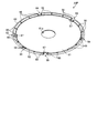
次に、回転プレート23Pの構成について図4および図5を用いて説明する。図4は、回転プレート23Pの斜視図であり、図5は、回転プレート23Pの平面図である。
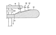
次に、上述した支持部材66の作用について説明する。図12は、本実施形態に係る回転プレート23PにおけるウェハWとの接触部分を拡大した模式断面図である。
次に、本実施形態に係る処理ユニット16の変形例について説明する。まず、第1変形例について図13を参照して説明する。図13は、第1変形例に係る乾燥促進処理の動作例を示す図である。
16 処理ユニット
23 ウェハ保持回転部
23P 回転プレート
61 第1平坦部
62 傾斜部
63 第2平坦部
64 第1切欠部
65 第2切欠部
66 支持部材
67 嵩上げ部
Claims (8)
- 基板の下方に配置され、前記基板の外側から前記基板の内側に向かって下り傾斜し且つ前記基板の周方向に沿って延在する傾斜面を有する傾斜部と、
前記傾斜面に対して突出して設けられ、前記基板を下方から支持する複数の支持部材と、
前記複数の支持部材に支持された前記基板の上面に処理液を供給する処理液供給部と、
前記傾斜部を回転させる回転機構と
を備え、
前記複数の支持部材は、
前記基板の外側から前記基板の内側に向かって延在する長細形状を有すること
を特徴とする液処理装置。 - 前記基板を側方から把持する複数の把持部
を備え、
前記傾斜部は、
前記傾斜面の外周縁のうち前記複数の把持部に対応する各部分を切り欠いた複数の第1切欠部
を備え、
前記第1切欠部の両側に前記複数の支持部材のうち2つが設けられること
を特徴とする請求項1に記載の液処理装置。 - 前記基板を上方へ持ち上げて前記複数の支持部材から離隔させる複数のリフトピン
を備え、
前記傾斜部は、
前記傾斜面の外周縁のうち前記複数のリフトピンに対応する各部分を切り欠いた複数の第2切欠部
を備え、
前記第2切欠部の両側に前記複数の支持部材のうち2つが設けられること
を特徴とする請求項1または2に記載の液処理装置。 - 前記傾斜部は、
前記第2切欠部および前記第2切欠部の両側に設けられる2つの前記支持部材に連接し、前記第2切欠部よりも径方向内側に位置する部分を嵩上げした嵩上げ部
を備えることを特徴とする請求項3に記載の液処理装置。 - 前記複数の支持部材は、
前記基板の径方向に沿って延在すること
を特徴とする請求項1〜4のいずれか一つに記載の液処理装置。 - 前記複数の支持部材は、
長手方向における両端部のうち前記基板の径方向外側に位置する端部を前記基板の径方向内側に位置する端部よりも前記回転機構による前記基板の回転方向後方側にずらした形状を有すること
を特徴とする請求項1〜4のいずれか一つに記載の液処理装置。 - 前記複数の支持部材に支持された前記基板の上面をブラシにより洗浄するブラシ洗浄部
を備え、
前記複数の支持部材は、
パターン形成面を下方に向けた前記基板を下方から支持すること
を特徴とする請求項1〜6のいずれか一つに記載の液処理装置。 - 前記基板を上方へ持ち上げて前記複数の支持部材から離隔させる複数のリフトピンと、
前記傾斜部よりも径方向内側から前記基板の下面に対して気体を供給する気体供給部と、
前記処理液供給部を用いて前記基板を処理した後、前記複数のリフトピンを用いて前記基板を前記複数の支持部材から離隔させた状態で、前記気体供給部を用いて前記基板の下面に対して気体を供給する制御部と
を備えることを特徴とする請求項1に記載の液処理装置。
Priority Applications (4)
| Application Number | Priority Date | Filing Date | Title |
|---|---|---|---|
| JP2016063210A JP6513048B2 (ja) | 2016-03-28 | 2016-03-28 | 液処理装置 |
| KR1020170028960A KR102294642B1 (ko) | 2016-03-28 | 2017-03-07 | 액 처리 장치 |
| US15/454,108 US10665478B2 (en) | 2016-03-28 | 2017-03-09 | Liquid processing apparatus |
| CN201710145062.5A CN107240566B (zh) | 2016-03-28 | 2017-03-10 | 液处理装置 |
Applications Claiming Priority (1)
| Application Number | Priority Date | Filing Date | Title |
|---|---|---|---|
| JP2016063210A JP6513048B2 (ja) | 2016-03-28 | 2016-03-28 | 液処理装置 |
Publications (2)
| Publication Number | Publication Date |
|---|---|
| JP2017183310A true JP2017183310A (ja) | 2017-10-05 |
| JP6513048B2 JP6513048B2 (ja) | 2019-05-15 |
Family
ID=59896686
Family Applications (1)
| Application Number | Title | Priority Date | Filing Date |
|---|---|---|---|
| JP2016063210A Active JP6513048B2 (ja) | 2016-03-28 | 2016-03-28 | 液処理装置 |
Country Status (4)
| Country | Link |
|---|---|
| US (1) | US10665478B2 (ja) |
| JP (1) | JP6513048B2 (ja) |
| KR (1) | KR102294642B1 (ja) |
| CN (1) | CN107240566B (ja) |
Cited By (3)
| Publication number | Priority date | Publication date | Assignee | Title |
|---|---|---|---|---|
| KR20190096267A (ko) * | 2018-02-08 | 2019-08-19 | 가부시키가이샤 스크린 홀딩스 | 기판 처리 장치 및 기판 처리 방법 |
| KR20200018253A (ko) | 2018-08-09 | 2020-02-19 | 도쿄엘렉트론가부시키가이샤 | 기판 처리 장치 및 기판 처리 방법 |
| KR20240165874A (ko) | 2023-05-16 | 2024-11-25 | 도쿄엘렉트론가부시키가이샤 | 기판 처리 장치 |
Families Citing this family (4)
| Publication number | Priority date | Publication date | Assignee | Title |
|---|---|---|---|---|
| JP6836913B2 (ja) * | 2017-01-17 | 2021-03-03 | 東京エレクトロン株式会社 | 基板処理装置、基板処理方法、及び記憶媒体 |
| CN110291602B (zh) | 2017-02-17 | 2021-12-10 | 株式会社村田制作所 | 固体电解电容器及其制造方法 |
| JP7205458B2 (ja) * | 2019-12-25 | 2023-01-17 | 株式会社Sumco | 気相成長装置 |
| JP7738507B2 (ja) * | 2022-03-24 | 2025-09-12 | 株式会社Screenホールディングス | 基板処理装置 |
Citations (3)
| Publication number | Priority date | Publication date | Assignee | Title |
|---|---|---|---|---|
| JP2004119542A (ja) * | 2002-09-25 | 2004-04-15 | Dainippon Screen Mfg Co Ltd | 基板処理装置および基板処理システム |
| WO2010109848A1 (ja) * | 2009-03-26 | 2010-09-30 | パナソニック株式会社 | プラズマ処理装置及びプラズマ処理方法 |
| JP2015211203A (ja) * | 2014-04-30 | 2015-11-24 | 東京エレクトロン株式会社 | 基板処理装置、基板処理装置の基板検知方法および記憶媒体 |
Family Cites Families (6)
| Publication number | Priority date | Publication date | Assignee | Title |
|---|---|---|---|---|
| JP3963817B2 (ja) * | 2002-10-28 | 2007-08-22 | 大日本スクリーン製造株式会社 | 基板処理装置および基板処理システム |
| JP4723001B2 (ja) * | 2006-10-05 | 2011-07-13 | 東京エレクトロン株式会社 | 基板処理装置、基板処理方法、および排液カップの洗浄方法 |
| JP5390824B2 (ja) | 2008-10-10 | 2014-01-15 | 大日本スクリーン製造株式会社 | 基板処理装置 |
| JP5726686B2 (ja) * | 2011-09-08 | 2015-06-03 | 東京エレクトロン株式会社 | 液処理装置、及び液処理装置の制御方法 |
| JP6234027B2 (ja) * | 2012-12-14 | 2017-11-22 | キヤノン株式会社 | 画像形成装置 |
| TWM505052U (zh) * | 2015-01-22 | 2015-07-11 | Scientech Corp | 流體製程處理裝置 |
-
2016
- 2016-03-28 JP JP2016063210A patent/JP6513048B2/ja active Active
-
2017
- 2017-03-07 KR KR1020170028960A patent/KR102294642B1/ko active Active
- 2017-03-09 US US15/454,108 patent/US10665478B2/en active Active
- 2017-03-10 CN CN201710145062.5A patent/CN107240566B/zh active Active
Patent Citations (3)
| Publication number | Priority date | Publication date | Assignee | Title |
|---|---|---|---|---|
| JP2004119542A (ja) * | 2002-09-25 | 2004-04-15 | Dainippon Screen Mfg Co Ltd | 基板処理装置および基板処理システム |
| WO2010109848A1 (ja) * | 2009-03-26 | 2010-09-30 | パナソニック株式会社 | プラズマ処理装置及びプラズマ処理方法 |
| JP2015211203A (ja) * | 2014-04-30 | 2015-11-24 | 東京エレクトロン株式会社 | 基板処理装置、基板処理装置の基板検知方法および記憶媒体 |
Cited By (7)
| Publication number | Priority date | Publication date | Assignee | Title |
|---|---|---|---|---|
| KR20190096267A (ko) * | 2018-02-08 | 2019-08-19 | 가부시키가이샤 스크린 홀딩스 | 기판 처리 장치 및 기판 처리 방법 |
| JP2019140210A (ja) * | 2018-02-08 | 2019-08-22 | 株式会社Screenホールディングス | 基板処理装置および基板処理方法 |
| KR102128176B1 (ko) | 2018-02-08 | 2020-06-29 | 가부시키가이샤 스크린 홀딩스 | 기판 처리 장치 및 기판 처리 방법 |
| US11361979B2 (en) | 2018-02-08 | 2022-06-14 | SCREEN Holdings Co., Ltd. | Substrate processing apparatus and substrate processing method |
| JP7116550B2 (ja) | 2018-02-08 | 2022-08-10 | 株式会社Screenホールディングス | 基板処理装置および基板処理方法 |
| KR20200018253A (ko) | 2018-08-09 | 2020-02-19 | 도쿄엘렉트론가부시키가이샤 | 기판 처리 장치 및 기판 처리 방법 |
| KR20240165874A (ko) | 2023-05-16 | 2024-11-25 | 도쿄엘렉트론가부시키가이샤 | 기판 처리 장치 |
Also Published As
| Publication number | Publication date |
|---|---|
| CN107240566B (zh) | 2021-12-14 |
| JP6513048B2 (ja) | 2019-05-15 |
| US10665478B2 (en) | 2020-05-26 |
| KR102294642B1 (ko) | 2021-08-27 |
| US20170278727A1 (en) | 2017-09-28 |
| CN107240566A (zh) | 2017-10-10 |
| KR20170113090A (ko) | 2017-10-12 |
Similar Documents
| Publication | Publication Date | Title |
|---|---|---|
| JP2017183310A (ja) | 液処理装置 | |
| TWI538044B (zh) | 用來清洗基板處理裝置的清洗治具及清洗方法、與基板處理系統 | |
| US10847387B2 (en) | Substrate processing apparatus, substrate processing method and recording medium | |
| JP2004207573A (ja) | 塗布処理装置 | |
| JP6258122B2 (ja) | 基板液処理装置、基板液処理方法及び記憶媒体 | |
| US11551941B2 (en) | Substrate cleaning method | |
| JP2013058607A (ja) | 液処理装置、及び液処理装置の制御方法 | |
| JP5072380B2 (ja) | 基板処理システム | |
| JP2018107292A (ja) | 基板処理方法および基板処理装置 | |
| KR20160094276A (ko) | 기판 처리 장치 및 기판 처리 방법 | |
| JP6395673B2 (ja) | 基板処理装置 | |
| JP5726637B2 (ja) | 液処理装置、液処理方法 | |
| JP6282988B2 (ja) | 基板処理装置、基板処理方法、及び記憶媒体 | |
| US11373883B2 (en) | Substrate processing apparatus, substrate processing system and substrate processing method | |
| JP6402087B2 (ja) | 液処理装置 | |
| JP6184890B2 (ja) | 基板液処理装置、基板液処理方法及び記憶媒体 | |
| JP5956946B2 (ja) | 液処理装置および液処理方法 | |
| JP5726636B2 (ja) | 液処理装置、液処理方法 | |
| JP2019201075A (ja) | 基板処理装置および基板処理方法 | |
| JP2018006647A (ja) | 基板液処理方法及び基板液処理装置 | |
| JP7138493B2 (ja) | 基板液処理方法、記憶媒体および基板液処理装置 | |
| WO2025047402A1 (ja) | 液処理装置および液処理方法 | |
| JP6184892B2 (ja) | 基板液処理装置、基板液処理方法及び記憶媒体 | |
| JP2015149496A (ja) | 液処理装置 | |
| JP2011035051A (ja) | 基板処理装置 |
Legal Events
| Date | Code | Title | Description |
|---|---|---|---|
| A621 | Written request for application examination |
Free format text: JAPANESE INTERMEDIATE CODE: A621 Effective date: 20171222 |
|
| A977 | Report on retrieval |
Free format text: JAPANESE INTERMEDIATE CODE: A971007 Effective date: 20180913 |
|
| A131 | Notification of reasons for refusal |
Free format text: JAPANESE INTERMEDIATE CODE: A131 Effective date: 20180925 |
|
| A521 | Request for written amendment filed |
Free format text: JAPANESE INTERMEDIATE CODE: A523 Effective date: 20181120 |
|
| TRDD | Decision of grant or rejection written | ||
| A01 | Written decision to grant a patent or to grant a registration (utility model) |
Free format text: JAPANESE INTERMEDIATE CODE: A01 Effective date: 20190312 |
|
| A61 | First payment of annual fees (during grant procedure) |
Free format text: JAPANESE INTERMEDIATE CODE: A61 Effective date: 20190409 |
|
| R150 | Certificate of patent or registration of utility model |
Ref document number: 6513048 Country of ref document: JP Free format text: JAPANESE INTERMEDIATE CODE: R150 |
|
| R250 | Receipt of annual fees |
Free format text: JAPANESE INTERMEDIATE CODE: R250 |
|
| R250 | Receipt of annual fees |
Free format text: JAPANESE INTERMEDIATE CODE: R250 |
|
| R250 | Receipt of annual fees |
Free format text: JAPANESE INTERMEDIATE CODE: R250 |
|
| R250 | Receipt of annual fees |
Free format text: JAPANESE INTERMEDIATE CODE: R250 |
|
| R250 | Receipt of annual fees |
Free format text: JAPANESE INTERMEDIATE CODE: R250 |