JP2017183604A - 炭化珪素半導体装置 - Google Patents
炭化珪素半導体装置 Download PDFInfo
- Publication number
- JP2017183604A JP2017183604A JP2016071217A JP2016071217A JP2017183604A JP 2017183604 A JP2017183604 A JP 2017183604A JP 2016071217 A JP2016071217 A JP 2016071217A JP 2016071217 A JP2016071217 A JP 2016071217A JP 2017183604 A JP2017183604 A JP 2017183604A
- Authority
- JP
- Japan
- Prior art keywords
- silicon carbide
- region
- semiconductor device
- trench
- carbide semiconductor
- Prior art date
- Legal status (The legal status is an assumption and is not a legal conclusion. Google has not performed a legal analysis and makes no representation as to the accuracy of the status listed.)
- Granted
Links
Images




Classifications
-
- H—ELECTRICITY
- H10—SEMICONDUCTOR DEVICES; ELECTRIC SOLID-STATE DEVICES NOT OTHERWISE PROVIDED FOR
- H10D—INORGANIC ELECTRIC SEMICONDUCTOR DEVICES
- H10D62/00—Semiconductor bodies, or regions thereof, of devices having potential barriers
- H10D62/10—Shapes, relative sizes or dispositions of the regions of the semiconductor bodies; Shapes of the semiconductor bodies
- H10D62/102—Constructional design considerations for preventing surface leakage or controlling electric field concentration
- H10D62/103—Constructional design considerations for preventing surface leakage or controlling electric field concentration for increasing or controlling the breakdown voltage of reverse-biased devices
- H10D62/105—Constructional design considerations for preventing surface leakage or controlling electric field concentration for increasing or controlling the breakdown voltage of reverse-biased devices by having particular doping profiles, shapes or arrangements of PN junctions; by having supplementary regions, e.g. junction termination extension [JTE]
- H10D62/109—Reduced surface field [RESURF] PN junction structures
-
- H—ELECTRICITY
- H10—SEMICONDUCTOR DEVICES; ELECTRIC SOLID-STATE DEVICES NOT OTHERWISE PROVIDED FOR
- H10D—INORGANIC ELECTRIC SEMICONDUCTOR DEVICES
- H10D12/00—Bipolar devices controlled by the field effect, e.g. insulated-gate bipolar transistors [IGBT]
-
- H—ELECTRICITY
- H10—SEMICONDUCTOR DEVICES; ELECTRIC SOLID-STATE DEVICES NOT OTHERWISE PROVIDED FOR
- H10D—INORGANIC ELECTRIC SEMICONDUCTOR DEVICES
- H10D12/00—Bipolar devices controlled by the field effect, e.g. insulated-gate bipolar transistors [IGBT]
- H10D12/411—Insulated-gate bipolar transistors [IGBT]
- H10D12/441—Vertical IGBTs
- H10D12/461—Vertical IGBTs having non-planar surfaces, e.g. having trenches, recesses or pillars in the surfaces of the emitter, base or collector regions
- H10D12/481—Vertical IGBTs having non-planar surfaces, e.g. having trenches, recesses or pillars in the surfaces of the emitter, base or collector regions having gate structures on slanted surfaces, on vertical surfaces, or in grooves, e.g. trench gate IGBTs
-
- H—ELECTRICITY
- H10—SEMICONDUCTOR DEVICES; ELECTRIC SOLID-STATE DEVICES NOT OTHERWISE PROVIDED FOR
- H10D—INORGANIC ELECTRIC SEMICONDUCTOR DEVICES
- H10D30/00—Field-effect transistors [FET]
- H10D30/60—Insulated-gate field-effect transistors [IGFET]
- H10D30/64—Double-diffused metal-oxide semiconductor [DMOS] FETs
- H10D30/66—Vertical DMOS [VDMOS] FETs
- H10D30/668—Vertical DMOS [VDMOS] FETs having trench gate electrodes, e.g. UMOS transistors
-
- H—ELECTRICITY
- H10—SEMICONDUCTOR DEVICES; ELECTRIC SOLID-STATE DEVICES NOT OTHERWISE PROVIDED FOR
- H10D—INORGANIC ELECTRIC SEMICONDUCTOR DEVICES
- H10D62/00—Semiconductor bodies, or regions thereof, of devices having potential barriers
- H10D62/10—Shapes, relative sizes or dispositions of the regions of the semiconductor bodies; Shapes of the semiconductor bodies
- H10D62/102—Constructional design considerations for preventing surface leakage or controlling electric field concentration
- H10D62/103—Constructional design considerations for preventing surface leakage or controlling electric field concentration for increasing or controlling the breakdown voltage of reverse-biased devices
- H10D62/105—Constructional design considerations for preventing surface leakage or controlling electric field concentration for increasing or controlling the breakdown voltage of reverse-biased devices by having particular doping profiles, shapes or arrangements of PN junctions; by having supplementary regions, e.g. junction termination extension [JTE]
- H10D62/106—Constructional design considerations for preventing surface leakage or controlling electric field concentration for increasing or controlling the breakdown voltage of reverse-biased devices by having particular doping profiles, shapes or arrangements of PN junctions; by having supplementary regions, e.g. junction termination extension [JTE] having supplementary regions doped oppositely to or in rectifying contact with regions of the semiconductor bodies, e.g. guard rings with PN or Schottky junctions
- H10D62/107—Buried supplementary regions, e.g. buried guard rings
-
- H—ELECTRICITY
- H10—SEMICONDUCTOR DEVICES; ELECTRIC SOLID-STATE DEVICES NOT OTHERWISE PROVIDED FOR
- H10D—INORGANIC ELECTRIC SEMICONDUCTOR DEVICES
- H10D62/00—Semiconductor bodies, or regions thereof, of devices having potential barriers
- H10D62/10—Shapes, relative sizes or dispositions of the regions of the semiconductor bodies; Shapes of the semiconductor bodies
- H10D62/13—Semiconductor regions connected to electrodes carrying current to be rectified, amplified or switched, e.g. source or drain regions
- H10D62/149—Source or drain regions of field-effect devices
- H10D62/151—Source or drain regions of field-effect devices of IGFETs
- H10D62/156—Drain regions of DMOS transistors
- H10D62/157—Impurity concentrations or distributions
-
- H—ELECTRICITY
- H10—SEMICONDUCTOR DEVICES; ELECTRIC SOLID-STATE DEVICES NOT OTHERWISE PROVIDED FOR
- H10D—INORGANIC ELECTRIC SEMICONDUCTOR DEVICES
- H10D62/00—Semiconductor bodies, or regions thereof, of devices having potential barriers
- H10D62/10—Shapes, relative sizes or dispositions of the regions of the semiconductor bodies; Shapes of the semiconductor bodies
- H10D62/17—Semiconductor regions connected to electrodes not carrying current to be rectified, amplified or switched, e.g. channel regions
- H10D62/393—Body regions of DMOS transistors or IGBTs
-
- H—ELECTRICITY
- H10—SEMICONDUCTOR DEVICES; ELECTRIC SOLID-STATE DEVICES NOT OTHERWISE PROVIDED FOR
- H10D—INORGANIC ELECTRIC SEMICONDUCTOR DEVICES
- H10D62/00—Semiconductor bodies, or regions thereof, of devices having potential barriers
- H10D62/80—Semiconductor bodies, or regions thereof, of devices having potential barriers characterised by the materials
- H10D62/81—Semiconductor bodies, or regions thereof, of devices having potential barriers characterised by the materials of structures exhibiting quantum-confinement effects, e.g. single quantum wells; of structures having periodic or quasi-periodic potential variation
-
- H—ELECTRICITY
- H10—SEMICONDUCTOR DEVICES; ELECTRIC SOLID-STATE DEVICES NOT OTHERWISE PROVIDED FOR
- H10D—INORGANIC ELECTRIC SEMICONDUCTOR DEVICES
- H10D62/00—Semiconductor bodies, or regions thereof, of devices having potential barriers
- H10D62/80—Semiconductor bodies, or regions thereof, of devices having potential barriers characterised by the materials
- H10D62/83—Semiconductor bodies, or regions thereof, of devices having potential barriers characterised by the materials being Group IV materials, e.g. B-doped Si or undoped Ge
- H10D62/832—Semiconductor bodies, or regions thereof, of devices having potential barriers characterised by the materials being Group IV materials, e.g. B-doped Si or undoped Ge being Group IV materials comprising two or more elements, e.g. SiGe
- H10D62/8325—Silicon carbide
-
- H—ELECTRICITY
- H10—SEMICONDUCTOR DEVICES; ELECTRIC SOLID-STATE DEVICES NOT OTHERWISE PROVIDED FOR
- H10D—INORGANIC ELECTRIC SEMICONDUCTOR DEVICES
- H10D64/00—Electrodes of devices having potential barriers
- H10D64/20—Electrodes characterised by their shapes, relative sizes or dispositions
- H10D64/27—Electrodes not carrying the current to be rectified, amplified, oscillated or switched, e.g. gates
- H10D64/311—Gate electrodes for field-effect devices
- H10D64/411—Gate electrodes for field-effect devices for FETs
- H10D64/511—Gate electrodes for field-effect devices for FETs for IGFETs
- H10D64/512—Disposition of the gate electrodes, e.g. buried gates
- H10D64/513—Disposition of the gate electrodes, e.g. buried gates within recesses in the substrate, e.g. trench gates, groove gates or buried gates
-
- H—ELECTRICITY
- H10—SEMICONDUCTOR DEVICES; ELECTRIC SOLID-STATE DEVICES NOT OTHERWISE PROVIDED FOR
- H10D—INORGANIC ELECTRIC SEMICONDUCTOR DEVICES
- H10D64/00—Electrodes of devices having potential barriers
- H10D64/20—Electrodes characterised by their shapes, relative sizes or dispositions
- H10D64/27—Electrodes not carrying the current to be rectified, amplified, oscillated or switched, e.g. gates
- H10D64/311—Gate electrodes for field-effect devices
- H10D64/411—Gate electrodes for field-effect devices for FETs
- H10D64/511—Gate electrodes for field-effect devices for FETs for IGFETs
- H10D64/514—Gate electrodes for field-effect devices for FETs for IGFETs characterised by the insulating layers
- H10D64/516—Gate electrodes for field-effect devices for FETs for IGFETs characterised by the insulating layers the thicknesses being non-uniform
-
- H—ELECTRICITY
- H10—SEMICONDUCTOR DEVICES; ELECTRIC SOLID-STATE DEVICES NOT OTHERWISE PROVIDED FOR
- H10D—INORGANIC ELECTRIC SEMICONDUCTOR DEVICES
- H10D64/00—Electrodes of devices having potential barriers
- H10D64/20—Electrodes characterised by their shapes, relative sizes or dispositions
- H10D64/27—Electrodes not carrying the current to be rectified, amplified, oscillated or switched, e.g. gates
- H10D64/311—Gate electrodes for field-effect devices
- H10D64/411—Gate electrodes for field-effect devices for FETs
- H10D64/511—Gate electrodes for field-effect devices for FETs for IGFETs
- H10D64/517—Gate electrodes for field-effect devices for FETs for IGFETs characterised by the conducting layers
- H10D64/518—Gate electrodes for field-effect devices for FETs for IGFETs characterised by the conducting layers characterised by their lengths or sectional shapes
Landscapes
- Electrodes Of Semiconductors (AREA)
Abstract
Description
以下、図面を参照しつつ、本発明の実施の形態について説明する。以下の説明では、同一または対応する要素には同一の符号を付して、それらについての詳細な説明は繰り返さない。
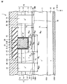
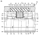
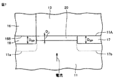
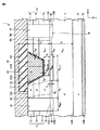
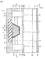
(1)本発明の一態様に係る炭化珪素半導体装置(1)は、炭化珪素基板(10)と、第1の炭化珪素層(11)と、第2の炭化珪素層(13)と、第3の炭化珪素層(14)と、第4の炭化珪素層(15)と、第1の不純物領域(16)とを備える。第1の炭化珪素層(11)は、炭化珪素基板(10)上に配置され、第1の導電型を有する。第2の炭化珪素層(13)は、第1の炭化珪素層(11)上に配置され、第1の導電型を有する。第3の炭化珪素層(14)は、第2の炭化珪素層(13)上に配置され、第1の導電型と異なる第2の導電型を有する。第4の炭化珪素層(15)は、第3の炭化珪素層(14)上に配置され、第1の導電型を有する。第1の不純物領域(16)は、第2の炭化珪素層(13)、第3の炭化珪素層(14)および第4の炭化珪素層(15)を貫通するように形成され、第2の導電型を有する。トレンチ(21)が、第4の炭化珪素層(15)から第3の炭化珪素層(14)を貫通して第2の炭化珪素層(13)に達するように、炭化珪素半導体装置(1)に形成される。炭化珪素半導体装置(1)は、トレンチ(21)の壁に接触したゲート絶縁膜(25)と、ゲート電極(30)と、第2の不純物領域(17)と、第3の不純物領域(18)と、第4の不純物領域(20)とを備える。ゲート電極(30)は、ゲート絶縁膜(25)に接触し、かつ、トレンチ(21)に充填される。第2の不純物領域(17)は、トレンチ(21)の下方にトレンチ(21)の底部から離間して配置され、第2の導電型を有する。第3の不純物領域(18)は、第1の不純物領域(16)に接するように第1の不純物領域(16)の下方に形成され、第2の導電型を有し、かつ、第2の不純物領域(17)に電気的に接続される。第4の不純物領域(20)は、第2の不純物領域(17)と第3の不純物領域(18)との間に形成され、第1の導電型を有する。
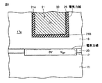
(4)上記(1)から(3)のいずれかの炭化珪素半導体装置において、トレンチ(21)の底部(21B)から第2の不純物領域(17)までの距離をD1と表すと、0.1μm≦D1≦3.0μmの関係が成り立つ。
(9)上記(1)から(8)のいずれかの炭化珪素半導体装置において、トレンチ(21)は、{0001}面に対して傾斜した側壁面(21A)を有する。
(10)上記(1)から(9)のいずれかの炭化珪素半導体装置は、MOSFETである。炭化珪素基板(10)は、第1の導電型を有する。
本発明の実施の形態に係る炭化珪素半導体装置の一例として、MOSFETが以下に例示される。
10 炭化珪素基板
10A,10B,12A 主面
11,12 炭化珪素エピタキシャル層
11A 界面
11a,13a,17a,17b 空乏層
13 ドリフト領域
14 ボディ領域
14a チャネル
15 ソース領域
16 ディープ領域
16B 底部(ディープ領域)
17,18,20 埋込領域
21 トレンチ
21A 側壁面
21B 底部(トレンチ)
25 ゲート絶縁膜
30 ゲート電極
40 層間絶縁膜
50 ソース電極
70 ドレイン電極
D1 距離
DBP,DJ 深さ
NBP,ND1,ND2,NJ 不純物濃度
WBP1,WBP2,WJ,Wtrench 幅
t1,t2,tg1,tg2 厚さ
Claims (11)
- 炭化珪素半導体装置であって、
炭化珪素基板と、
前記炭化珪素基板上に配置され、第1の導電型を有する、第1の炭化珪素層と、
前記第1の炭化珪素層上に配置され、前記第1の導電型を有する第2の炭化珪素層と、
前記第2の炭化珪素層上に配置され、前記第1の導電型と異なる第2の導電型を有する、第3の炭化珪素層と、
前記第3の炭化珪素層上に配置され、前記第1の導電型を有する、第4の炭化珪素層と、
前記第2の炭化珪素層、前記第3の炭化珪素層および前記第4の炭化珪素層を貫通するように形成され、前記第2の導電型を有する第1の不純物領域とを備え、
トレンチが、前記第4の炭化珪素層から前記第3の炭化珪素層を貫通して前記第2の炭化珪素層に達するように、前記炭化珪素半導体装置に形成され、
前記炭化珪素半導体装置は、
前記トレンチの壁に接触したゲート絶縁膜と、
前記ゲート絶縁膜に接触し、かつ、前記トレンチに充填されたゲート電極と、
前記トレンチの下方に前記トレンチの底部から離間して配置され、前記第2の導電型を有する、第2の不純物領域と、
前記第1の不純物領域に接するように前記第1の不純物領域の下方に形成され、前記第2の導電型を有し、かつ、前記第2の不純物領域に電気的に接続された第3の不純物領域と、
前記第2の不純物領域と前記第3の不純物領域との間に形成され、前記第1の導電型を有する第4の不純物領域とを備える、炭化珪素半導体装置。 - 前記第2の炭化珪素層の不純物濃度は、前記第1の炭化珪素層の不純物濃度よりも大きく、
前記第4の不純物領域の不純物濃度は、前記第2の炭化珪素層の不純物濃度よりも大きく、
前記第2の不純物領域の不純物濃度は、前記第4の不純物領域の不純物濃度よりも大きい、請求項1に記載の炭化珪素半導体装置。 - 前記第1の炭化珪素層と前記第2の炭化珪素層との界面からの前記第4の不純物領域の深さは、前記界面からの前記第2の不純物領域の深さよりも小さい、請求項1または請求項2に記載の炭化珪素半導体装置。
- 前記トレンチの前記底部から前記第2の不純物領域までの距離をD1と表すと、
0.1μm≦D1≦3.0μm
の関係が成り立つ、請求項1から請求項3のいずれか1項に記載の炭化珪素半導体装置。 - 前記第3の不純物領域の横方向の幅は、前記第2の不純物領域の横方向の幅よりも小さい、請求項1から請求項4のいずれか1項に記載の炭化珪素半導体装置。
- 前記第2の不純物領域の横方向の幅は、前記トレンチの横方向の幅よりも大きい、請求項1から請求項5のいずれか1項に記載の炭化珪素半導体装置。
- 前記トレンチの底部における前記ゲート絶縁膜の厚さは、前記トレンチの側壁に接する前記ゲート絶縁膜の部分の厚さよりも大きい、請求項1から請求項6のいずれか1項に記載の炭化珪素半導体装置。
- 前記トレンチの側壁の結晶面方位が<1−100>または<11−20>である、請求項1から請求項7のいずれか1項に記載の炭化珪素半導体装置。
- 前記トレンチは、{000−1}面に対して傾斜した側壁面を有する、請求項1から請求項8のいずれか1項に記載の炭化珪素半導体装置。
- 前記炭化珪素半導体装置は、MOSFETであり、
前記炭化珪素基板は、前記第1の導電型を有する、請求項1から請求項9のいずれか1項に記載の炭化珪素半導体装置。 - 前記炭化珪素半導体装置は、IGBTであり、
前記炭化珪素基板は、前記第2の導電型を有する、請求項1から請求項9のいずれか1項に記載の炭化珪素半導体装置。
Priority Applications (3)
| Application Number | Priority Date | Filing Date | Title |
|---|---|---|---|
| JP2016071217A JP6708954B2 (ja) | 2016-03-31 | 2016-03-31 | 炭化珪素半導体装置 |
| US16/089,448 US10756168B2 (en) | 2016-03-31 | 2017-02-02 | Silicon carbide semiconductor device |
| PCT/JP2017/003712 WO2017169085A1 (ja) | 2016-03-31 | 2017-02-02 | 炭化珪素半導体装置 |
Applications Claiming Priority (1)
| Application Number | Priority Date | Filing Date | Title |
|---|---|---|---|
| JP2016071217A JP6708954B2 (ja) | 2016-03-31 | 2016-03-31 | 炭化珪素半導体装置 |
Publications (2)
| Publication Number | Publication Date |
|---|---|
| JP2017183604A true JP2017183604A (ja) | 2017-10-05 |
| JP6708954B2 JP6708954B2 (ja) | 2020-06-10 |
Family
ID=59963844
Family Applications (1)
| Application Number | Title | Priority Date | Filing Date |
|---|---|---|---|
| JP2016071217A Active JP6708954B2 (ja) | 2016-03-31 | 2016-03-31 | 炭化珪素半導体装置 |
Country Status (3)
| Country | Link |
|---|---|
| US (1) | US10756168B2 (ja) |
| JP (1) | JP6708954B2 (ja) |
| WO (1) | WO2017169085A1 (ja) |
Cited By (5)
| Publication number | Priority date | Publication date | Assignee | Title |
|---|---|---|---|---|
| CN110098258A (zh) * | 2018-01-29 | 2019-08-06 | 瑞萨电子株式会社 | 半导体器件及其制造方法 |
| JP2019140259A (ja) * | 2018-02-09 | 2019-08-22 | 富士電機株式会社 | 半導体装置および半導体装置の製造方法 |
| JP2021141265A (ja) * | 2020-03-09 | 2021-09-16 | 三菱電機株式会社 | 半導体装置 |
| JP2022534924A (ja) * | 2019-05-27 | 2022-08-04 | ロベルト・ボッシュ・ゲゼルシャフト・ミト・ベシュレンクテル・ハフツング | パワートランジスタの製造方法およびパワートランジスタ |
| JP2023087028A (ja) * | 2018-10-30 | 2023-06-22 | ローム株式会社 | 半導体装置 |
Families Citing this family (9)
| Publication number | Priority date | Publication date | Assignee | Title |
|---|---|---|---|---|
| JP6658406B2 (ja) * | 2016-08-31 | 2020-03-04 | 株式会社デンソー | 炭化珪素半導体装置の製造方法 |
| WO2018088063A1 (ja) * | 2016-11-11 | 2018-05-17 | 住友電気工業株式会社 | 炭化珪素半導体装置 |
| JP7073873B2 (ja) * | 2018-04-13 | 2022-05-24 | 株式会社デンソー | スイッチング素子 |
| GB2589543A (en) * | 2019-09-09 | 2021-06-09 | Mqsemi Ag | Method for forming a low injection P-type contact region and power semiconductor devices with the same |
| CN114556588B (zh) * | 2019-10-11 | 2025-08-19 | 株式会社电装 | 开关元件 |
| JP7662431B2 (ja) * | 2021-06-29 | 2025-04-15 | 株式会社豊田中央研究所 | 半導体装置 |
| CN113990919A (zh) * | 2021-10-12 | 2022-01-28 | 松山湖材料实验室 | 碳化硅半导体结构、器件及制备方法 |
| US20240234495A1 (en) * | 2023-01-05 | 2024-07-11 | Wolfspeed, Inc. | Gate trench power semiconductor devices having self-aligned trench shielding regions and related methods |
| CN119208385B (zh) * | 2024-11-26 | 2025-05-02 | 安徽长飞先进半导体股份有限公司 | 半导体器件及制备方法、功率模块、功率转换电路和车辆 |
Citations (11)
| Publication number | Priority date | Publication date | Assignee | Title |
|---|---|---|---|---|
| JP2009117593A (ja) * | 2007-11-06 | 2009-05-28 | Denso Corp | 炭化珪素半導体装置およびその製造方法 |
| JP2011100967A (ja) * | 2009-07-21 | 2011-05-19 | Rohm Co Ltd | 半導体装置 |
| JP2012038770A (ja) * | 2010-08-03 | 2012-02-23 | Sumitomo Electric Ind Ltd | 半導体装置およびその製造方法 |
| JP2013145770A (ja) * | 2012-01-13 | 2013-07-25 | Sumitomo Electric Ind Ltd | 半導体装置およびその製造方法 |
| JP2013219161A (ja) * | 2012-04-09 | 2013-10-24 | Mitsubishi Electric Corp | 半導体装置および半導体装置の製造方法 |
| JP2014053595A (ja) * | 2012-08-07 | 2014-03-20 | Denso Corp | 炭化珪素半導体装置およびその製造方法 |
| JP2015026726A (ja) * | 2013-07-26 | 2015-02-05 | 住友電気工業株式会社 | 炭化珪素半導体装置およびその製造方法 |
| JP2015220408A (ja) * | 2014-05-20 | 2015-12-07 | 住友電気工業株式会社 | 炭化珪素半導体装置およびその製造方法 |
| WO2016002766A1 (ja) * | 2014-06-30 | 2016-01-07 | 国立研究開発法人産業技術総合研究所 | 炭化珪素半導体装置およびその製造方法 |
| WO2016002769A1 (ja) * | 2014-06-30 | 2016-01-07 | 国立研究開発法人産業技術総合研究所 | 炭化珪素半導体装置およびその製造方法 |
| WO2016038833A1 (ja) * | 2014-09-08 | 2016-03-17 | パナソニックIpマネジメント株式会社 | 半導体装置及びその製造方法 |
Family Cites Families (4)
| Publication number | Priority date | Publication date | Assignee | Title |
|---|---|---|---|---|
| JP2012099601A (ja) | 2010-11-01 | 2012-05-24 | Sumitomo Electric Ind Ltd | 半導体装置およびその製造方法 |
| WO2012077617A1 (ja) | 2010-12-10 | 2012-06-14 | 三菱電機株式会社 | 半導体装置およびその製造方法 |
| JP2013069964A (ja) | 2011-09-26 | 2013-04-18 | Sumitomo Electric Ind Ltd | 炭化珪素半導体装置 |
| JP6111673B2 (ja) | 2012-07-25 | 2017-04-12 | 住友電気工業株式会社 | 炭化珪素半導体装置 |
-
2016
- 2016-03-31 JP JP2016071217A patent/JP6708954B2/ja active Active
-
2017
- 2017-02-02 US US16/089,448 patent/US10756168B2/en active Active
- 2017-02-02 WO PCT/JP2017/003712 patent/WO2017169085A1/ja not_active Ceased
Patent Citations (11)
| Publication number | Priority date | Publication date | Assignee | Title |
|---|---|---|---|---|
| JP2009117593A (ja) * | 2007-11-06 | 2009-05-28 | Denso Corp | 炭化珪素半導体装置およびその製造方法 |
| JP2011100967A (ja) * | 2009-07-21 | 2011-05-19 | Rohm Co Ltd | 半導体装置 |
| JP2012038770A (ja) * | 2010-08-03 | 2012-02-23 | Sumitomo Electric Ind Ltd | 半導体装置およびその製造方法 |
| JP2013145770A (ja) * | 2012-01-13 | 2013-07-25 | Sumitomo Electric Ind Ltd | 半導体装置およびその製造方法 |
| JP2013219161A (ja) * | 2012-04-09 | 2013-10-24 | Mitsubishi Electric Corp | 半導体装置および半導体装置の製造方法 |
| JP2014053595A (ja) * | 2012-08-07 | 2014-03-20 | Denso Corp | 炭化珪素半導体装置およびその製造方法 |
| JP2015026726A (ja) * | 2013-07-26 | 2015-02-05 | 住友電気工業株式会社 | 炭化珪素半導体装置およびその製造方法 |
| JP2015220408A (ja) * | 2014-05-20 | 2015-12-07 | 住友電気工業株式会社 | 炭化珪素半導体装置およびその製造方法 |
| WO2016002766A1 (ja) * | 2014-06-30 | 2016-01-07 | 国立研究開発法人産業技術総合研究所 | 炭化珪素半導体装置およびその製造方法 |
| WO2016002769A1 (ja) * | 2014-06-30 | 2016-01-07 | 国立研究開発法人産業技術総合研究所 | 炭化珪素半導体装置およびその製造方法 |
| WO2016038833A1 (ja) * | 2014-09-08 | 2016-03-17 | パナソニックIpマネジメント株式会社 | 半導体装置及びその製造方法 |
Cited By (8)
| Publication number | Priority date | Publication date | Assignee | Title |
|---|---|---|---|---|
| CN110098258A (zh) * | 2018-01-29 | 2019-08-06 | 瑞萨电子株式会社 | 半导体器件及其制造方法 |
| JP2019140259A (ja) * | 2018-02-09 | 2019-08-22 | 富士電機株式会社 | 半導体装置および半導体装置の製造方法 |
| JP7106882B2 (ja) | 2018-02-09 | 2022-07-27 | 富士電機株式会社 | 半導体装置および半導体装置の製造方法 |
| JP2023087028A (ja) * | 2018-10-30 | 2023-06-22 | ローム株式会社 | 半導体装置 |
| JP7536140B2 (ja) | 2018-10-30 | 2024-08-19 | ローム株式会社 | 半導体装置 |
| JP2022534924A (ja) * | 2019-05-27 | 2022-08-04 | ロベルト・ボッシュ・ゲゼルシャフト・ミト・ベシュレンクテル・ハフツング | パワートランジスタの製造方法およびパワートランジスタ |
| JP2021141265A (ja) * | 2020-03-09 | 2021-09-16 | 三菱電機株式会社 | 半導体装置 |
| JP7442932B2 (ja) | 2020-03-09 | 2024-03-05 | 三菱電機株式会社 | 半導体装置 |
Also Published As
| Publication number | Publication date |
|---|---|
| WO2017169085A1 (ja) | 2017-10-05 |
| US10756168B2 (en) | 2020-08-25 |
| US20190237536A1 (en) | 2019-08-01 |
| JP6708954B2 (ja) | 2020-06-10 |
Similar Documents
| Publication | Publication Date | Title |
|---|---|---|
| JP6708954B2 (ja) | 炭化珪素半導体装置 | |
| JP6400778B2 (ja) | 絶縁ゲート型炭化珪素半導体装置及びその製造方法 | |
| JP6197995B2 (ja) | ワイドバンドギャップ絶縁ゲート型半導体装置 | |
| JP5668576B2 (ja) | 炭化珪素半導体装置 | |
| JP5840308B2 (ja) | 炭化珪素半導体装置およびその製造方法 | |
| JP6323556B2 (ja) | 半導体装置 | |
| JP2001135819A (ja) | 超接合半導体素子 | |
| JP5297706B2 (ja) | 半導体装置 | |
| JP7139678B2 (ja) | 炭化ケイ素半導体装置 | |
| WO2015141212A1 (ja) | 半導体装置 | |
| JP7051890B2 (ja) | ワイドギャップ半導体装置 | |
| JP6291988B2 (ja) | 炭化珪素半導体装置 | |
| US10199457B2 (en) | Silicon carbide semiconductor device | |
| JP4595327B2 (ja) | 半導体素子 | |
| CN107710401A (zh) | 半导体装置 | |
| US20150171169A1 (en) | Semiconductor device | |
| JP2015162578A (ja) | ワイドバンドギャップ半導体装置およびその製造方法 | |
| CN113614883B (zh) | 半导体装置 | |
| JP6651801B2 (ja) | 半導体装置および半導体装置の製造方法 | |
| JP7207361B2 (ja) | 半導体装置 | |
| JP2005093809A (ja) | 半導体装置 | |
| JP2014192242A (ja) | 半導体装置 | |
| JP5082260B2 (ja) | 炭化珪素半導体装置 |
Legal Events
| Date | Code | Title | Description |
|---|---|---|---|
| A621 | Written request for application examination |
Free format text: JAPANESE INTERMEDIATE CODE: A621 Effective date: 20181022 |
|
| A131 | Notification of reasons for refusal |
Free format text: JAPANESE INTERMEDIATE CODE: A131 Effective date: 20191217 |
|
| A521 | Request for written amendment filed |
Free format text: JAPANESE INTERMEDIATE CODE: A523 Effective date: 20200120 |
|
| TRDD | Decision of grant or rejection written | ||
| A01 | Written decision to grant a patent or to grant a registration (utility model) |
Free format text: JAPANESE INTERMEDIATE CODE: A01 Effective date: 20200422 |
|
| A61 | First payment of annual fees (during grant procedure) |
Free format text: JAPANESE INTERMEDIATE CODE: A61 Effective date: 20200505 |
|
| R150 | Certificate of patent or registration of utility model |
Ref document number: 6708954 Country of ref document: JP Free format text: JAPANESE INTERMEDIATE CODE: R150 |
|
| R250 | Receipt of annual fees |
Free format text: JAPANESE INTERMEDIATE CODE: R250 |
|
| R250 | Receipt of annual fees |
Free format text: JAPANESE INTERMEDIATE CODE: R250 |
|
| R250 | Receipt of annual fees |
Free format text: JAPANESE INTERMEDIATE CODE: R250 |
|
| R250 | Receipt of annual fees |
Free format text: JAPANESE INTERMEDIATE CODE: R250 |
|
| S111 | Request for change of ownership or part of ownership |
Free format text: JAPANESE INTERMEDIATE CODE: R313113 |