JP2017188625A - 金属化フィルムコンデンサとその製造方法、および金属化フィルム積層体 - Google Patents
金属化フィルムコンデンサとその製造方法、および金属化フィルム積層体 Download PDFInfo
- Publication number
- JP2017188625A JP2017188625A JP2016078183A JP2016078183A JP2017188625A JP 2017188625 A JP2017188625 A JP 2017188625A JP 2016078183 A JP2016078183 A JP 2016078183A JP 2016078183 A JP2016078183 A JP 2016078183A JP 2017188625 A JP2017188625 A JP 2017188625A
- Authority
- JP
- Japan
- Prior art keywords
- metallized film
- metallized
- film
- films
- film capacitor
- Prior art date
- Legal status (The legal status is an assumption and is not a legal conclusion. Google has not performed a legal analysis and makes no representation as to the accuracy of the status listed.)
- Granted
Links
Images






Classifications
-
- H—ELECTRICITY
- H01—ELECTRIC ELEMENTS
- H01G—CAPACITORS; CAPACITORS, RECTIFIERS, DETECTORS, SWITCHING DEVICES, LIGHT-SENSITIVE OR TEMPERATURE-SENSITIVE DEVICES OF THE ELECTROLYTIC TYPE
- H01G4/00—Fixed capacitors; Processes of their manufacture
- H01G4/33—Thin- or thick-film capacitors (thin- or thick-film circuits; capacitors without a potential-jump or surface barrier specially adapted for integrated circuits, details thereof, multistep manufacturing processes therefor)
-
- B—PERFORMING OPERATIONS; TRANSPORTING
- B32—LAYERED PRODUCTS
- B32B—LAYERED PRODUCTS, i.e. PRODUCTS BUILT-UP OF STRATA OF FLAT OR NON-FLAT, e.g. CELLULAR OR HONEYCOMB, FORM
- B32B15/00—Layered products comprising a layer of metal
- B32B15/01—Layered products comprising a layer of metal all layers being exclusively metallic
-
- B—PERFORMING OPERATIONS; TRANSPORTING
- B32—LAYERED PRODUCTS
- B32B—LAYERED PRODUCTS, i.e. PRODUCTS BUILT-UP OF STRATA OF FLAT OR NON-FLAT, e.g. CELLULAR OR HONEYCOMB, FORM
- B32B27/00—Layered products comprising a layer of synthetic resin
- B32B27/06—Layered products comprising a layer of synthetic resin as the main or only constituent of a layer, which is next to another layer of the same or of a different material
- B32B27/08—Layered products comprising a layer of synthetic resin as the main or only constituent of a layer, which is next to another layer of the same or of a different material of synthetic resin
-
- B—PERFORMING OPERATIONS; TRANSPORTING
- B32—LAYERED PRODUCTS
- B32B—LAYERED PRODUCTS, i.e. PRODUCTS BUILT-UP OF STRATA OF FLAT OR NON-FLAT, e.g. CELLULAR OR HONEYCOMB, FORM
- B32B27/00—Layered products comprising a layer of synthetic resin
- B32B27/18—Layered products comprising a layer of synthetic resin characterised by the use of special additives
- B32B27/20—Layered products comprising a layer of synthetic resin characterised by the use of special additives using fillers, pigments, thixotroping agents
-
- B—PERFORMING OPERATIONS; TRANSPORTING
- B32—LAYERED PRODUCTS
- B32B—LAYERED PRODUCTS, i.e. PRODUCTS BUILT-UP OF STRATA OF FLAT OR NON-FLAT, e.g. CELLULAR OR HONEYCOMB, FORM
- B32B27/00—Layered products comprising a layer of synthetic resin
- B32B27/30—Layered products comprising a layer of synthetic resin comprising vinyl (co)polymers; comprising acrylic (co)polymers
- B32B27/304—Layered products comprising a layer of synthetic resin comprising vinyl (co)polymers; comprising acrylic (co)polymers comprising vinyl halide (co)polymers, e.g. PVC, PVDC, PVF, PVDF
-
- B—PERFORMING OPERATIONS; TRANSPORTING
- B32—LAYERED PRODUCTS
- B32B—LAYERED PRODUCTS, i.e. PRODUCTS BUILT-UP OF STRATA OF FLAT OR NON-FLAT, e.g. CELLULAR OR HONEYCOMB, FORM
- B32B3/00—Layered products comprising a layer with external or internal discontinuities or unevennesses, or a layer of non-planar shape; Layered products comprising a layer having particular features of form
- B32B3/02—Layered products comprising a layer with external or internal discontinuities or unevennesses, or a layer of non-planar shape; Layered products comprising a layer having particular features of form characterised by features of form at particular places, e.g. in edge regions
-
- B—PERFORMING OPERATIONS; TRANSPORTING
- B32—LAYERED PRODUCTS
- B32B—LAYERED PRODUCTS, i.e. PRODUCTS BUILT-UP OF STRATA OF FLAT OR NON-FLAT, e.g. CELLULAR OR HONEYCOMB, FORM
- B32B3/00—Layered products comprising a layer with external or internal discontinuities or unevennesses, or a layer of non-planar shape; Layered products comprising a layer having particular features of form
- B32B3/02—Layered products comprising a layer with external or internal discontinuities or unevennesses, or a layer of non-planar shape; Layered products comprising a layer having particular features of form characterised by features of form at particular places, e.g. in edge regions
- B32B3/08—Layered products comprising a layer with external or internal discontinuities or unevennesses, or a layer of non-planar shape; Layered products comprising a layer having particular features of form characterised by features of form at particular places, e.g. in edge regions characterised by added members at particular parts
-
- B—PERFORMING OPERATIONS; TRANSPORTING
- B32—LAYERED PRODUCTS
- B32B—LAYERED PRODUCTS, i.e. PRODUCTS BUILT-UP OF STRATA OF FLAT OR NON-FLAT, e.g. CELLULAR OR HONEYCOMB, FORM
- B32B3/00—Layered products comprising a layer with external or internal discontinuities or unevennesses, or a layer of non-planar shape; Layered products comprising a layer having particular features of form
- B32B3/26—Layered products comprising a layer with external or internal discontinuities or unevennesses, or a layer of non-planar shape; Layered products comprising a layer having particular features of form characterised by a particular shape of the outline of the cross-section of a continuous layer; characterised by a layer with cavities or internal voids ; characterised by an apertured layer
- B32B3/28—Layered products comprising a layer with external or internal discontinuities or unevennesses, or a layer of non-planar shape; Layered products comprising a layer having particular features of form characterised by a particular shape of the outline of the cross-section of a continuous layer; characterised by a layer with cavities or internal voids ; characterised by an apertured layer characterised by a layer comprising a deformed thin sheet, i.e. the layer having its entire thickness deformed out of the plane, e.g. corrugated, crumpled
-
- H—ELECTRICITY
- H01—ELECTRIC ELEMENTS
- H01G—CAPACITORS; CAPACITORS, RECTIFIERS, DETECTORS, SWITCHING DEVICES, LIGHT-SENSITIVE OR TEMPERATURE-SENSITIVE DEVICES OF THE ELECTROLYTIC TYPE
- H01G13/00—Apparatus specially adapted for manufacturing capacitors; Processes specially adapted for manufacturing capacitors not provided for in groups H01G4/00 - H01G11/00
- H01G13/02—Machines for winding capacitors
-
- H—ELECTRICITY
- H01—ELECTRIC ELEMENTS
- H01G—CAPACITORS; CAPACITORS, RECTIFIERS, DETECTORS, SWITCHING DEVICES, LIGHT-SENSITIVE OR TEMPERATURE-SENSITIVE DEVICES OF THE ELECTROLYTIC TYPE
- H01G4/00—Fixed capacitors; Processes of their manufacture
- H01G4/002—Details
- H01G4/005—Electrodes
- H01G4/015—Special provisions for self-healing
-
- H—ELECTRICITY
- H01—ELECTRIC ELEMENTS
- H01G—CAPACITORS; CAPACITORS, RECTIFIERS, DETECTORS, SWITCHING DEVICES, LIGHT-SENSITIVE OR TEMPERATURE-SENSITIVE DEVICES OF THE ELECTROLYTIC TYPE
- H01G4/00—Fixed capacitors; Processes of their manufacture
- H01G4/002—Details
- H01G4/018—Dielectrics
- H01G4/06—Solid dielectrics
- H01G4/14—Organic dielectrics
- H01G4/18—Organic dielectrics of synthetic material, e.g. derivatives of cellulose
-
- H—ELECTRICITY
- H01—ELECTRIC ELEMENTS
- H01G—CAPACITORS; CAPACITORS, RECTIFIERS, DETECTORS, SWITCHING DEVICES, LIGHT-SENSITIVE OR TEMPERATURE-SENSITIVE DEVICES OF THE ELECTROLYTIC TYPE
- H01G4/00—Fixed capacitors; Processes of their manufacture
- H01G4/002—Details
- H01G4/228—Terminals
-
- H—ELECTRICITY
- H01—ELECTRIC ELEMENTS
- H01G—CAPACITORS; CAPACITORS, RECTIFIERS, DETECTORS, SWITCHING DEVICES, LIGHT-SENSITIVE OR TEMPERATURE-SENSITIVE DEVICES OF THE ELECTROLYTIC TYPE
- H01G4/00—Fixed capacitors; Processes of their manufacture
- H01G4/30—Stacked capacitors
- H01G4/306—Stacked capacitors made by thin film techniques
-
- H—ELECTRICITY
- H01—ELECTRIC ELEMENTS
- H01G—CAPACITORS; CAPACITORS, RECTIFIERS, DETECTORS, SWITCHING DEVICES, LIGHT-SENSITIVE OR TEMPERATURE-SENSITIVE DEVICES OF THE ELECTROLYTIC TYPE
- H01G4/00—Fixed capacitors; Processes of their manufacture
- H01G4/32—Wound capacitors
-
- B—PERFORMING OPERATIONS; TRANSPORTING
- B32—LAYERED PRODUCTS
- B32B—LAYERED PRODUCTS, i.e. PRODUCTS BUILT-UP OF STRATA OF FLAT OR NON-FLAT, e.g. CELLULAR OR HONEYCOMB, FORM
- B32B37/00—Methods or apparatus for laminating, e.g. by curing or by ultrasonic bonding
- B32B37/14—Methods or apparatus for laminating, e.g. by curing or by ultrasonic bonding characterised by the properties of the layers
- B32B37/24—Methods or apparatus for laminating, e.g. by curing or by ultrasonic bonding characterised by the properties of the layers with at least one layer not being coherent before laminating, e.g. made up from granular material sprinkled onto a substrate
- B32B2037/246—Vapour deposition
-
- B—PERFORMING OPERATIONS; TRANSPORTING
- B32—LAYERED PRODUCTS
- B32B—LAYERED PRODUCTS, i.e. PRODUCTS BUILT-UP OF STRATA OF FLAT OR NON-FLAT, e.g. CELLULAR OR HONEYCOMB, FORM
- B32B2250/00—Layers arrangement
- B32B2250/02—2 layers
-
- B—PERFORMING OPERATIONS; TRANSPORTING
- B32—LAYERED PRODUCTS
- B32B—LAYERED PRODUCTS, i.e. PRODUCTS BUILT-UP OF STRATA OF FLAT OR NON-FLAT, e.g. CELLULAR OR HONEYCOMB, FORM
- B32B2255/00—Coating on the layer surface
- B32B2255/06—Coating on the layer surface on metal layer
-
- B—PERFORMING OPERATIONS; TRANSPORTING
- B32—LAYERED PRODUCTS
- B32B—LAYERED PRODUCTS, i.e. PRODUCTS BUILT-UP OF STRATA OF FLAT OR NON-FLAT, e.g. CELLULAR OR HONEYCOMB, FORM
- B32B2255/00—Coating on the layer surface
- B32B2255/10—Coating on the layer surface on synthetic resin layer or on natural or synthetic rubber layer
-
- B—PERFORMING OPERATIONS; TRANSPORTING
- B32—LAYERED PRODUCTS
- B32B—LAYERED PRODUCTS, i.e. PRODUCTS BUILT-UP OF STRATA OF FLAT OR NON-FLAT, e.g. CELLULAR OR HONEYCOMB, FORM
- B32B2255/00—Coating on the layer surface
- B32B2255/20—Inorganic coating
- B32B2255/205—Metallic coating
-
- B—PERFORMING OPERATIONS; TRANSPORTING
- B32—LAYERED PRODUCTS
- B32B—LAYERED PRODUCTS, i.e. PRODUCTS BUILT-UP OF STRATA OF FLAT OR NON-FLAT, e.g. CELLULAR OR HONEYCOMB, FORM
- B32B2307/00—Properties of the layers or laminate
- B32B2307/20—Properties of the layers or laminate having particular electrical or magnetic properties, e.g. piezoelectric
- B32B2307/204—Di-electric
-
- B—PERFORMING OPERATIONS; TRANSPORTING
- B32—LAYERED PRODUCTS
- B32B—LAYERED PRODUCTS, i.e. PRODUCTS BUILT-UP OF STRATA OF FLAT OR NON-FLAT, e.g. CELLULAR OR HONEYCOMB, FORM
- B32B2307/00—Properties of the layers or laminate
- B32B2307/50—Properties of the layers or laminate having particular mechanical properties
-
- B—PERFORMING OPERATIONS; TRANSPORTING
- B32—LAYERED PRODUCTS
- B32B—LAYERED PRODUCTS, i.e. PRODUCTS BUILT-UP OF STRATA OF FLAT OR NON-FLAT, e.g. CELLULAR OR HONEYCOMB, FORM
- B32B2307/00—Properties of the layers or laminate
- B32B2307/70—Other properties
- B32B2307/744—Non-slip, anti-slip
-
- B—PERFORMING OPERATIONS; TRANSPORTING
- B32—LAYERED PRODUCTS
- B32B—LAYERED PRODUCTS, i.e. PRODUCTS BUILT-UP OF STRATA OF FLAT OR NON-FLAT, e.g. CELLULAR OR HONEYCOMB, FORM
- B32B2307/00—Properties of the layers or laminate
- B32B2307/70—Other properties
- B32B2307/746—Slipping, anti-blocking, low friction
-
- B—PERFORMING OPERATIONS; TRANSPORTING
- B32—LAYERED PRODUCTS
- B32B—LAYERED PRODUCTS, i.e. PRODUCTS BUILT-UP OF STRATA OF FLAT OR NON-FLAT, e.g. CELLULAR OR HONEYCOMB, FORM
- B32B2307/00—Properties of the layers or laminate
- B32B2307/70—Other properties
- B32B2307/762—Self-repairing, self-healing
-
- B—PERFORMING OPERATIONS; TRANSPORTING
- B32—LAYERED PRODUCTS
- B32B—LAYERED PRODUCTS, i.e. PRODUCTS BUILT-UP OF STRATA OF FLAT OR NON-FLAT, e.g. CELLULAR OR HONEYCOMB, FORM
- B32B2457/00—Electrical equipment
- B32B2457/16—Capacitors
-
- B—PERFORMING OPERATIONS; TRANSPORTING
- B32—LAYERED PRODUCTS
- B32B—LAYERED PRODUCTS, i.e. PRODUCTS BUILT-UP OF STRATA OF FLAT OR NON-FLAT, e.g. CELLULAR OR HONEYCOMB, FORM
- B32B37/00—Methods or apparatus for laminating, e.g. by curing or by ultrasonic bonding
- B32B37/14—Methods or apparatus for laminating, e.g. by curing or by ultrasonic bonding characterised by the properties of the layers
- B32B37/16—Methods or apparatus for laminating, e.g. by curing or by ultrasonic bonding characterised by the properties of the layers with all layers existing as coherent layers before laminating
- B32B37/18—Methods or apparatus for laminating, e.g. by curing or by ultrasonic bonding characterised by the properties of the layers with all layers existing as coherent layers before laminating involving the assembly of discrete sheets or panels only
-
- B—PERFORMING OPERATIONS; TRANSPORTING
- B32—LAYERED PRODUCTS
- B32B—LAYERED PRODUCTS, i.e. PRODUCTS BUILT-UP OF STRATA OF FLAT OR NON-FLAT, e.g. CELLULAR OR HONEYCOMB, FORM
- B32B38/00—Ancillary operations in connection with laminating processes
- B32B38/06—Embossing
Landscapes
- Engineering & Computer Science (AREA)
- Power Engineering (AREA)
- Microelectronics & Electronic Packaging (AREA)
- Manufacturing & Machinery (AREA)
- Fixed Capacitors And Capacitor Manufacturing Machines (AREA)
- Chemical & Material Sciences (AREA)
- Chemical Kinetics & Catalysis (AREA)
- Materials Engineering (AREA)
- Mechanical Engineering (AREA)
- Metallurgy (AREA)
- Organic Chemistry (AREA)
Abstract
Description
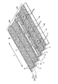
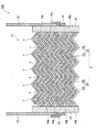
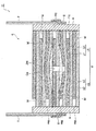
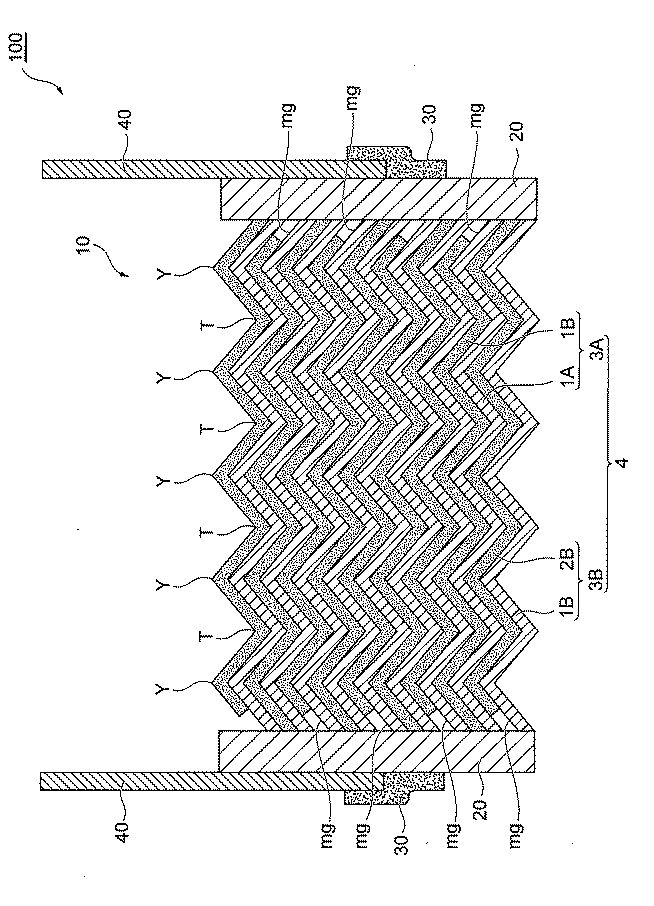
図1,2はその順に本発明の金属化フィルムコンデンサの製造方法の第1のステップを説明した模式図であり、図3は製作された金属化フィルムを示した模式図である。また、図4,5はその順に金属化フィルムコンデンサの製造方法の第2のステップを説明した模式図であり、図6は金属化フィルムコンデンサの製造方法の第3のステップを説明した模式図であって、製造された金属化フィルムコンデンサを示した図である。
本発明者等は、金属化フィルムコンデンサの加工性と自己回復機能を検証する実験をおこなった。以下、表1に、実施例1〜3と比較例1〜3の仕様と、加工性および自己回復性に関する実験結果を示す。
Claims (4)
- 複数の非蒸着スリット、および非蒸着スリット間に介在するヒューズ部を備えた金属蒸着膜と、ポリフッ化ビニリデン(PVDF)製の誘電体フィルムと、からなる2つの金属化フィルムが重ね合わされ、巻き回されて形成されている金属化フィルム柱体と、
前記金属化フィルム柱体の2つの電極取り出し面に形成されている金属溶射部と、
それぞれの前記金属溶射部に接合されている外部引き出し端子と、からなり、
前記金属化フィルムは、巻き回し方向に直交する断面形状が、傾斜した山部と谷部が連続した形状を有しており、
複数の前記金属化フィルムの山部同士が対応し、谷部同士が対応して積層されている、金属化フィルムコンデンサ。 - 前記山部の水平線からの傾斜角度θが60度以上である請求項1に記載の金属化フィルムコンデンサ。
- ポリフッ化ビニリデン(PVDF)製の誘電体フィルムの表面に、複数の非蒸着スリット、および非蒸着スリット間に介在するヒューズ部を備えた金属蒸着膜を形成して金属化フィルム中間体を製作し、
前記金属化フィルム中間体に対し、該金属化フィルム中間体が巻き回し方向に直交する断面形状を、傾斜した山部と谷部が連続した形状にして金属化フィルムを製作する第1のステップ、
2つの前記金属化フィルムを、山部同士を対応させ、谷部同士を対応させて積層し、巻き回して金属化フィルム柱体を製作する第2のステップ、
前記金属化フィルム柱体の2つの電極取り出し面に金属溶射部を形成し、該金属溶射部に外部引き出し端子を接合して金属化フィルムコンデンサを製造する第3のステップからなる、金属化フィルムコンデンサの製造方法。 - 複数の非蒸着スリット、および非蒸着スリット間に介在するヒューズ部を備えた金属蒸着膜と、ポリフッ化ビニリデン(PVDF)製の誘電体フィルムと、からなる2つの金属化フィルムが重ね合わされ、巻き回されて形成される、巻回し型の金属化フィルムコンデンサに適用される金属化フィルム積層体であって、
前記金属化フィルムは、巻き回し方向に直交する断面形状が、傾斜した山部と谷部が連続した形状を有しており、
複数の前記金属化フィルムの山部同士が対応し、谷部同士が対応して積層されている金属化フィルム積層体。
Priority Applications (3)
| Application Number | Priority Date | Filing Date | Title |
|---|---|---|---|
| JP2016078183A JP6380450B2 (ja) | 2016-04-08 | 2016-04-08 | 金属化フィルムコンデンサとその製造方法、および金属化フィルム積層体 |
| CN201710196397.XA CN107275084B (zh) | 2016-04-08 | 2017-03-29 | 金属化薄膜电容器及其制造方法以及金属化薄膜层叠体 |
| US15/478,288 US10079107B2 (en) | 2016-04-08 | 2017-04-04 | Metallized film capacitor, manufacturing method of metallized film capacitor, and metallized film laminate |
Applications Claiming Priority (1)
| Application Number | Priority Date | Filing Date | Title |
|---|---|---|---|
| JP2016078183A JP6380450B2 (ja) | 2016-04-08 | 2016-04-08 | 金属化フィルムコンデンサとその製造方法、および金属化フィルム積層体 |
Publications (2)
| Publication Number | Publication Date |
|---|---|
| JP2017188625A true JP2017188625A (ja) | 2017-10-12 |
| JP6380450B2 JP6380450B2 (ja) | 2018-08-29 |
Family
ID=59999582
Family Applications (1)
| Application Number | Title | Priority Date | Filing Date |
|---|---|---|---|
| JP2016078183A Active JP6380450B2 (ja) | 2016-04-08 | 2016-04-08 | 金属化フィルムコンデンサとその製造方法、および金属化フィルム積層体 |
Country Status (3)
| Country | Link |
|---|---|
| US (1) | US10079107B2 (ja) |
| JP (1) | JP6380450B2 (ja) |
| CN (1) | CN107275084B (ja) |
Families Citing this family (6)
| Publication number | Priority date | Publication date | Assignee | Title |
|---|---|---|---|---|
| JP6356936B2 (ja) * | 2016-07-26 | 2018-07-11 | 京セラ株式会社 | フィルムコンデンサ、連結型コンデンサ、インバータおよび電動車輌 |
| CN111341557B (zh) * | 2020-04-07 | 2024-11-12 | 深圳汇北川科技股份有限公司 | 一种用于电容器的金属化膜和电容器 |
| CN111808311A (zh) * | 2020-06-24 | 2020-10-23 | 西安交通大学 | 一种聚丙烯-聚偏氟乙烯复合金属化薄膜及其制备方法 |
| CN114121488B (zh) * | 2021-10-29 | 2024-04-05 | 安徽赛福电容有限公司 | 金属化薄膜及其制造方法、制造装置和电容器 |
| CN114005678A (zh) * | 2021-11-03 | 2022-02-01 | 安徽赛福电子有限公司 | 金属化薄膜电容器及其制造方法以及金属化薄膜层叠体 |
| CN116089880B (zh) * | 2023-02-11 | 2024-01-05 | 重庆大学 | 一种金属化薄膜电容器初始自愈类型分类方法及系统 |
Citations (7)
| Publication number | Priority date | Publication date | Assignee | Title |
|---|---|---|---|---|
| JPS504563A (ja) * | 1973-05-16 | 1975-01-17 | ||
| JPS5498956A (en) * | 1978-01-21 | 1979-08-04 | Nichicon Capacitor Ltd | Oillpregnated condenser |
| JPS5689240U (ja) * | 1979-12-13 | 1981-07-16 | ||
| JPS5896720A (ja) * | 1981-12-04 | 1983-06-08 | 株式会社東芝 | コンデンサ |
| JPH0179818U (ja) * | 1987-11-16 | 1989-05-29 | ||
| JPH02106912A (ja) * | 1988-10-17 | 1990-04-19 | Matsushita Electric Ind Co Ltd | 積層フィルムコンデンサ |
| JP2015053331A (ja) * | 2013-09-05 | 2015-03-19 | トヨタ自動車株式会社 | フィルムコンデンサ |
Family Cites Families (6)
| Publication number | Priority date | Publication date | Assignee | Title |
|---|---|---|---|---|
| JP4366930B2 (ja) | 2002-12-20 | 2009-11-18 | パナソニック株式会社 | 金属化フィルムコンデンサ |
| US7933111B2 (en) * | 2007-05-08 | 2011-04-26 | Nuinteck Co., Ltd | Metallized plastic film and film capacitor |
| JP5954280B2 (ja) * | 2013-08-30 | 2016-07-20 | トヨタ自動車株式会社 | 金属化フィルム |
| JP6321419B2 (ja) | 2014-03-24 | 2018-05-09 | 京セラ株式会社 | フィルムコンデンサ |
| JP6064956B2 (ja) * | 2014-09-16 | 2017-01-25 | トヨタ自動車株式会社 | フィルムコンデンサ |
| CN104878348A (zh) * | 2015-04-21 | 2015-09-02 | 浙江七星电容器有限公司 | 超薄型金属化电容蒸镀膜及其制备工艺 |
-
2016
- 2016-04-08 JP JP2016078183A patent/JP6380450B2/ja active Active
-
2017
- 2017-03-29 CN CN201710196397.XA patent/CN107275084B/zh active Active
- 2017-04-04 US US15/478,288 patent/US10079107B2/en active Active
Patent Citations (7)
| Publication number | Priority date | Publication date | Assignee | Title |
|---|---|---|---|---|
| JPS504563A (ja) * | 1973-05-16 | 1975-01-17 | ||
| JPS5498956A (en) * | 1978-01-21 | 1979-08-04 | Nichicon Capacitor Ltd | Oillpregnated condenser |
| JPS5689240U (ja) * | 1979-12-13 | 1981-07-16 | ||
| JPS5896720A (ja) * | 1981-12-04 | 1983-06-08 | 株式会社東芝 | コンデンサ |
| JPH0179818U (ja) * | 1987-11-16 | 1989-05-29 | ||
| JPH02106912A (ja) * | 1988-10-17 | 1990-04-19 | Matsushita Electric Ind Co Ltd | 積層フィルムコンデンサ |
| JP2015053331A (ja) * | 2013-09-05 | 2015-03-19 | トヨタ自動車株式会社 | フィルムコンデンサ |
Also Published As
| Publication number | Publication date |
|---|---|
| CN107275084B (zh) | 2019-02-12 |
| US20170294269A1 (en) | 2017-10-12 |
| JP6380450B2 (ja) | 2018-08-29 |
| CN107275084A (zh) | 2017-10-20 |
| US10079107B2 (en) | 2018-09-18 |
Similar Documents
| Publication | Publication Date | Title |
|---|---|---|
| JP6380450B2 (ja) | 金属化フィルムコンデンサとその製造方法、および金属化フィルム積層体 | |
| JP2013247206A (ja) | フィルムコンデンサ素子及びフィルムコンデンサ並びにフィルムコンデンサ素子の製造方法 | |
| JP6356936B2 (ja) | フィルムコンデンサ、連結型コンデンサ、インバータおよび電動車輌 | |
| CN104040656B (zh) | 薄膜电容器 | |
| WO2002101770A1 (fr) | Condensateur de fil metallise | |
| WO2010090245A1 (ja) | 金属化フィルムコンデンサ | |
| JP6383933B1 (ja) | 金属化フィルム、版ロール | |
| JP6064956B2 (ja) | フィルムコンデンサ | |
| JP2015201527A (ja) | 金属化フィルムコンデンサ | |
| JP6748851B2 (ja) | 金属化フィルムコンデンサ | |
| JP2013247207A (ja) | フィルムコンデンサ素子の製造方法 | |
| JP6330139B2 (ja) | 金属化フィルムコンデンサ | |
| JP7079150B2 (ja) | コンデンサ素子用の金属化フィルムおよびそれを用いた金属化フィルムコンデンサ | |
| JP2012009764A (ja) | フィルムコンデンサ | |
| JP6321414B2 (ja) | フィルムコンデンサ | |
| JP2006286988A (ja) | 金属化フィルムコンデンサ | |
| US10522286B2 (en) | Dielectric film and film capacitor | |
| JP2016046291A (ja) | フィルムコンデンサ素子及びその製造方法 | |
| JP2015198232A (ja) | 金属化フィルムコンデンサ | |
| JPH0687453B2 (ja) | コンデンサ | |
| JPH02222129A (ja) | フィルムコンデンサおよびその製造方法 | |
| JPH10199751A (ja) | メタライズドフィルムおよびフィルムコンデンサ | |
| JP2737896B2 (ja) | 保安機能付きコンデンサ用金属化基体 | |
| JP6413781B2 (ja) | 金属化フィルムコンデンサ | |
| WO2025177793A1 (ja) | フィルムコンデンサ、金属化フィルム及び金属化フィルムの製造方法 |
Legal Events
| Date | Code | Title | Description |
|---|---|---|---|
| A621 | Written request for application examination |
Free format text: JAPANESE INTERMEDIATE CODE: A621 Effective date: 20170721 |
|
| A977 | Report on retrieval |
Free format text: JAPANESE INTERMEDIATE CODE: A971007 Effective date: 20180619 |
|
| TRDD | Decision of grant or rejection written | ||
| A01 | Written decision to grant a patent or to grant a registration (utility model) |
Free format text: JAPANESE INTERMEDIATE CODE: A01 Effective date: 20180703 |
|
| A61 | First payment of annual fees (during grant procedure) |
Free format text: JAPANESE INTERMEDIATE CODE: A61 Effective date: 20180716 |
|
| R151 | Written notification of patent or utility model registration |
Ref document number: 6380450 Country of ref document: JP Free format text: JAPANESE INTERMEDIATE CODE: R151 |