JP2017191143A - Optical scanner and image forming apparatus including the same - Google Patents
Optical scanner and image forming apparatus including the same Download PDFInfo
- Publication number
- JP2017191143A JP2017191143A JP2016079045A JP2016079045A JP2017191143A JP 2017191143 A JP2017191143 A JP 2017191143A JP 2016079045 A JP2016079045 A JP 2016079045A JP 2016079045 A JP2016079045 A JP 2016079045A JP 2017191143 A JP2017191143 A JP 2017191143A
- Authority
- JP
- Japan
- Prior art keywords
- optical
- scanning device
- light beam
- deflector
- light
- Prior art date
- Legal status (The legal status is an assumption and is not a legal conclusion. Google has not performed a legal analysis and makes no representation as to the accuracy of the status listed.)
- Pending
Links
Images



Landscapes
- Laser Beam Printer (AREA)
- Mechanical Optical Scanning Systems (AREA)
- Lenses (AREA)
- Color Electrophotography (AREA)
- Facsimile Scanning Arrangements (AREA)
Abstract
Description
本発明は光走査装置に関し、例えば、レーザービームプリンタ(LBP)やデジタル複写機、マルチファンクションプリンタ(多機能プリンタ)等の画像形成装置に好適なものである。 The present invention relates to an optical scanning apparatus, and is suitable for an image forming apparatus such as a laser beam printer (LBP), a digital copying machine, or a multifunction printer (multifunction printer).
画像形成装置が備える光走査装置として、光源から出射した光束を偏向器により偏向し、偏向された光束を結像光学系によって被走査面に導光することにより、被走査面を主走査方向に光走査するものが知られている。このような光走査装置において、被走査面を高精度に光走査するためには、偏向器により偏向された光束を同期検知して、被走査面での主走査方向における走査開始位置を決定するための同期検知部が必要になる。 As an optical scanning device provided in an image forming apparatus, a light beam emitted from a light source is deflected by a deflector, and the deflected light beam is guided to a scanned surface by an imaging optical system, thereby moving the scanned surface in the main scanning direction. What scans light is known. In such an optical scanning device, in order to optically scan the surface to be scanned with high accuracy, the light beam deflected by the deflector is synchronously detected to determine the scanning start position in the main scanning direction on the surface to be scanned. A synchronization detector is required.
特許文献1には、偏向器により偏向されて結像光学系に入射する前の軸外光束を、ミラーにより反射させることで同期検知部に導光する構成が記載されている。この構成によれば、偏向器からの光束を、結像光学系の端部を通過させることなく同期検知部に導光することができるため、主走査断面内において偏向器及び結像光学系を小型化することが可能になる。 Patent Document 1 describes a configuration in which an off-axis light beam before being incident on the imaging optical system after being deflected by a deflector is guided to a synchronization detection unit by being reflected by a mirror. According to this configuration, since the light beam from the deflector can be guided to the synchronization detection unit without passing through the end of the imaging optical system, the deflector and the imaging optical system are arranged in the main scanning section. It becomes possible to reduce the size.
しかしながら、特許文献1に記載の構成では、配置誤差や環境変動(温度変化)などによりミラーの姿勢が設計値からずれた場合、ミラーにて反射した光束の到達位置が設計位置から大幅にずれてしまう。この場合、高精度な同期検知ができなくなり、良好な画像が得られなくなってしまう可能性がある。 However, in the configuration described in Patent Document 1, when the mirror posture deviates from the design value due to an arrangement error or environmental variation (temperature change), the arrival position of the light beam reflected by the mirror deviates significantly from the design position. End up. In this case, highly accurate synchronization detection cannot be performed, and a good image may not be obtained.
本発明の目的は、小型でかつ高精度な同期検知を実現可能な光走査装置及び画像形成装置を提供することである。 An object of the present invention is to provide an optical scanning device and an image forming apparatus that are small and can realize highly accurate synchronous detection.
上記目的を達成するための、本発明の一側面としての光走査装置は、光束を偏向して被走査面を主走査方向に光走査する偏向器と、該偏向器により偏向された光束を前記被走査面に導光する結像光学系と、前記偏向器により偏向された光束を受光して信号を生成する受光部と、前記偏向器により偏向された光束の主光線を、主走査断面内において前記結像光学系から離れる方向に屈折させて、前記受光部の受光面に導光する屈折光学素子と、を備え、主走査断面内において、前記偏向器の偏向面から前記屈折光学素子の入射面までの距離をLBD、前記受光面の中心に向かうときの前記屈折光学素子に入射する光束の主光線と前記結像光学系の光軸との成す角度をθBD、前記偏向面から前記結像光学系の最も前記偏向面に近い光学面までの距離をLs、とするとき、LBD×cosθBD≦Lsなる条件を満足することを特徴とする。 In order to achieve the above object, an optical scanning device according to one aspect of the present invention includes a deflector that deflects a light beam and optically scans a surface to be scanned in a main scanning direction, and the light beam deflected by the deflector. An imaging optical system that guides light to a surface to be scanned, a light receiving unit that receives a light beam deflected by the deflector and generates a signal, and a principal ray of the light beam deflected by the deflector within the main scanning section. A refracting optical element that refracts in a direction away from the imaging optical system and guides the light to the light receiving surface of the light receiving unit, and from the deflection surface of the deflector within the main scanning section, The distance to the incident surface is L BD , the angle formed between the principal ray of the light beam incident on the refractive optical element when going to the center of the light receiving surface and the optical axis of the imaging optical system is θ BD , from the deflection surface To the optical surface closest to the deflection surface of the imaging optical system When the distance Ls, and, and satisfies the L BD × cosθ BD ≦ Ls following condition.
本発明によれば、小型でかつ高精度な同期検知を実現可能な光走査装置及び画像形成装置を提供することができる。 According to the present invention, it is possible to provide an optical scanning device and an image forming apparatus that are small and can realize highly accurate synchronization detection.
以下、本発明の好ましい実施形態について図面を参照しながら説明する。なお、各図面は、便宜的に実際とは異なる縮尺で描かれている場合がある。また、各図面において、同一の部材については同一の参照番号を付し、重複する説明を省略する。 Hereinafter, preferred embodiments of the present invention will be described with reference to the drawings. Each drawing may be drawn on a different scale for convenience. Moreover, in each drawing, the same reference number is attached | subjected about the same member and the overlapping description is abbreviate | omitted.
なお、以下の説明において、主走査方向とは、後述する偏向器の回転軸と光学系の光軸方向とに垂直な方向であり、副走査方向とは、偏向器の回転軸に平行な方向である。また、主走査断面とは、光学系の光軸を含み主走査方向に平行な断面(副走査方向に垂直な断面)であり、副走査断面とは、副走査方向に平行な断面(主走査方向に垂直な断面)である。すなわち、これらの各方向及び各断面は、光学系毎に異なる場合がある。 In the following description, the main scanning direction is a direction perpendicular to the rotation axis of a deflector described later and the optical axis direction of the optical system, and the sub-scanning direction is a direction parallel to the rotation axis of the deflector. It is. The main scanning section is a section that includes the optical axis of the optical system and is parallel to the main scanning direction (cross section perpendicular to the sub scanning direction). The sub scanning section is a section that is parallel to the sub scanning direction (main scanning). Cross section perpendicular to the direction). That is, each direction and each cross section may be different for each optical system.
[実施例1]
以下、本発明の実施例1に係る光走査装置について詳細に説明する。
[Example 1]
Hereinafter, the optical scanning device according to the first embodiment of the present invention will be described in detail.
(光走査装置)
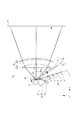
図1及び図2は、本発明の実施例1に係る光走査装置100の要部概略図であり、図1は主走査断面図(XY断面図)、図2は副走査断面図(ZX断面図)、を夫々示している。本実施例に係る光走査装置100は、光源1と、偏向器10と、結像光学系20と、同期検知部(BD光学系)30と、入射光学系40と、光量検知部50と、反射光学系60と、を備える。なお、図1では、反射光学系60を省略して光路を展開しており、図2では、偏向面10から被走査面17に至る光路に配置された部材以外を省略している。
(Optical scanning device)
1 and 2 are schematic views of a main part of an
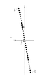
光源1は、複数の発光点を有するマルチビーム光源としての半導体レーザーである。図3に示すように、本発明に係る光源1は、主走査方向(Y方向)及び副走査方向(Z方向)において互いに離間して配置された32個の発光点LD1〜LD32を有する面発光レーザー(VCSEL)である。本実施例に係る各発光点は、主走査方向に対して角度αだけ傾いた直線上に配列(一次元配列)されているが、必要に応じて二次元配列されたものを採用してもよい。このように、マルチビーム光源を用いることで、光走査の高速化及び高精細化を実現することができる。 The light source 1 is a semiconductor laser as a multi-beam light source having a plurality of light emitting points. As shown in FIG. 3, the light source 1 according to the present invention has a surface emission having 32 light emitting points LD1 to LD32 which are arranged apart from each other in the main scanning direction (Y direction) and the sub scanning direction (Z direction). Laser (VCSEL). The light emitting points according to the present embodiment are arranged (one-dimensional arrangement) on a straight line inclined by an angle α with respect to the main scanning direction, but two-dimensional arrangement may be adopted as necessary. Good. As described above, by using the multi-beam light source, it is possible to realize high-speed and high-definition optical scanning.
入射光学系40は、光源1から出射した光束を偏向器10の偏向面10aに導光するための光学系であり、第1の絞り2と、コリメータレンズ3と、球面レンズ4と、シリンドリカルレンズ5と、第2の絞り6と、プリズム7と、を有する。
The incident
第1の絞り2は、副走査方向における光束の幅を制限する副走査絞りである。第1の絞り2をコリメータレンズ3の近傍に配置することにより、光走査装置100の全系の副走査断面内における射出瞳位置を、後述する結像レンズ20bの近傍に設定することができる。これにより、各発光点から出射した主光線の夫々が、結像レンズ20bの近傍で副走査方向における略同一の位置を通過するように構成することができる。
The first stop 2 is a sub-scanning stop that limits the width of the light beam in the sub-scanning direction. By disposing the first diaphragm 2 in the vicinity of the
コリメータレンズ3は、ガラスから成る凸レンズ及び凹レンズが互いに貼り合わされて構成された貼り合せレンズであり、球面レンズ4は、ガラスから成る凸球面レンズである。コリメータレンズ3及び球面レンズ4により、各発光点から出射した発散光束を略平行光束に変換し、被走査面17での各光束の径を揃えることができる。シリンドリカルレンズ5は、副走査断面内においてのみパワーを有するレンズであり、球面レンズ4を通過した光束を副走査断面内において集光し、主走査方向に長い線像を偏向面10aに形成している。なお、コリメータレンズ3とシリンドリカルレンズ5とを一体化して1つのレンズとしてもよい。
The
第2の絞り6は、主走査方向における光束の幅を制限する主走査絞りである。第2の絞り6を偏向面10aの近傍に配置することにより、各発光点からの光束の主光線を偏向面10aにおいて互いに近接させることができるため、被走査面17における主走査方向のジッター(縦線ゆらぎ)を低減することが可能になる。
The second diaphragm 6 is a main scanning diaphragm that limits the width of the light beam in the main scanning direction. By disposing the second diaphragm 6 in the vicinity of the
プリズム7は、光源1からの光束を、偏向器10の偏向面10aに向かう透過光束と、後述する光量検知部50に向かう反射光束と、に分岐させるための分岐光学素子である。具体的には、プリズム7は、主光線の通過位置での入射面の面法線と出射面の面法線とが、主走査断面内において4°の角度を成したくさび形状のウェッジプリズムである。なお、第2の絞り6は、プリズム7の入射面上に配置されている。
The prism 7 is a branching optical element for branching the light flux from the light source 1 into a transmitted light flux directed to the deflecting
光量検知部50は、プリズム7の入射面で反射した反射光束を集光する結像レンズ8と、結像レンズ8からの光束を受光する光量検知センサー9と、を含む。プリズム7は、出射面で反射した光束が光量検知部50に入射しないように構成されている。光量検知センサー9から出力される検出信号を、光源1の駆動回路にフィードバックすることで、光源1から出射する光束の強度を自動制御(オートパワーコントロール:APC)することができる。これにより、光源1の出力(発光光量)が常に設計値と等しくなるように制御することができるため、温度変化に依らず安定した画像形成を行うことが可能になる。
The light
偏向器10は、5つの偏向面10aを有するポリゴンミラー(回転多面鏡)であり、モータ等の駆動手段(不図示)により図1中の矢印Aの方向に一定速度で回転している。偏向器10は、入射光学系40により導光された光束を各偏向面10aにて偏向し、被走査面17における有効走査領域を主走査方向に等速度で光走査している。なお、偏向面10aの数は適宜選択し得るものである。また、偏向器10として、揺動軸を中心に一定速度で揺動する揺動ミラーなどを採用してもよい。
The
結像光学系20は、集光機能及びfθ特性を有するfθ光学系であり、2つの結像レンズ(結像光学素子)により構成されている。第1の結像レンズ20aはガラスから成る平凸球面レンズであり、第2の結像レンズ20bは主走査断面内において非円弧形状のレンズ面(光学面)を有するアナモフィックレンズである。本実施例では、結像光学系20を2枚の結像レンズにより構成しているが、必要に応じて1枚もしくは3枚以上の結像レンズを備える構成を採用してもよい。
The imaging
また、結像光学系20は、偏向器10によって偏向された光束(走査光束)を被走査面17に集光することで、各発光点のスポット像を形成している。さらに、結像光学系20は、副走査断面内において偏向面10aと被走査面17とを共役関係にすることにより、偏向面10aの面倒れ補正を行っている。
In addition, the imaging
本実施例に係る第1の結像レンズ20aについて、偏向器10の側のレンズ面(入射面)は平面であり、被走査面17の側のレンズ面(出射面)は、主走査断面内及び副走査断面内の両方において円弧形状である。一方、第2の結像レンズ20bの各レンズ面の主走査断面内での形状は、以下の式により表される。
In the
ここでは、各レンズ面と光軸との交点を原点とし、光軸をX軸、主走査断面内において光軸と直交する軸をY軸、副走査断面内において光軸と直交する軸をZ軸としている。また、Rは曲率半径、K、B4、B6、B8、B10は非球面係数であり、各係数の添え字sは走査開始側、eは走査終了側を表している。本実施例では、走査開始側と走査終了側とで非球面係数が一致しているため、各レンズ面の主走査断面内での形状は、光軸に対して対称となっている。 Here, the intersection of each lens surface and the optical axis is the origin, the optical axis is the X axis, the axis orthogonal to the optical axis in the main scanning section is the Y axis, and the axis orthogonal to the optical axis in the sub-scanning section is Z. The axis. R is a radius of curvature, K, B 4 , B 6 , B 8 , and B 10 are aspherical coefficients, the suffix s of each coefficient is the scanning start side, and e is the scanning end side. In the present embodiment, since the aspherical coefficients coincide on the scanning start side and the scanning end side, the shape of each lens surface in the main scanning section is symmetric with respect to the optical axis.
また、第2の結像レンズ20bの各レンズ面の副走査断面内での形状は、以下の式で表される。
In addition, the shape of each lens surface of the
ここで、r’は副走査断面内での曲率半径、rは副走査断面内での軸上における曲率半径、Miは非球面係数、D2、D4、D6、D8、D10は曲率変化係数、であり、各曲率変化係数の添え字sは走査開始側、eは走査終了側を表している。副走査断面内において、第2の結像レンズ20bの各レンズ面は円弧形状であり、各レンズ面の曲率は走査開始側から走査終了側にかけて連続的に変化している。
Here, r ′ is the radius of curvature in the sub-scan section, r is the radius of curvature on the axis in the sub-scan section, Mi is the aspheric coefficient, D 2 , D 4 , D 6 , D 8 , D 10 are Curvature change coefficient, the subscript s of each curvature change coefficient indicates the scanning start side, and e indicates the scanning end side. In the sub-scan section, each lens surface of the
反射光学系60は、2つの折り返しミラー(反射光学素子)により構成されている。図2に示すように、結像光学系20を通過した走査光束は、第1の折り返しミラー60a及び第2の折り返しミラー60bによって順に反射され、防塵ガラス16を介して被走査面17に導光される。このように、反射光学系60によって光路を折り曲げることにより、光走査装置100のX方向におけるサイズを縮小することが可能になる。
The reflection
表1に、本実施例に係る光走査装置100に関する各数値を示す。表1において、各断面内での入射角は、入射光学系40からの光束が偏向面10aに入射するときの入射角を示し、結像光学系20の焦点距離は、光軸上での値を示している。偏向器10の回転中心座標は、偏向面10aと像高0(軸上)の主光線との交点(軸上偏向点)を原点として示されている。また、偏向器10の回転角は、軸上光束を偏向するときの角度を0°とした場合の、最軸外光束を偏向するときの角度を示している。なお、表1において、dは面間隔、Nは屈折率、を夫々示している。
Table 1 shows numerical values related to the
(同期検知部)
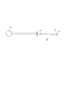
図4は、図1に示した同期検知部30の拡大図である。同期検知部30は、屈折光学素子としてのウェッジプリズム11と、BDレンズ(集光素子)12と、BDセンサー(受光部)13と、を有する。ウェッジプリズム11は、入射面の面法線と出射面の面法線とが、主走査断面内において互いに非平行であるくさび形状の光学素子である。具体的に、本実施例では、入射面の面法線と出射面の面法線とが主走査断面内において4°の角度を成している。また、BDレンズ12は、樹脂から成り、主走査断面内と副走査断面内とで互いに異なるパワーを有するアナモフィック面を含むアナモフィックレンズである。
(Synchronization detector)
FIG. 4 is an enlarged view of the
表2に、本実施例に係る同期検知部30に関する各数値を示す。
Table 2 shows numerical values related to the
図1に示したように、偏向器10の偏向面10aは矢印Aの方向に回転しているため、偏向面10aで偏向される光束は、結像光学系20を介して被走査面17を走査する前に、同期検知部30に入射する。このとき、同期検知部30に入射する光束(BD光束)の主光線は、ウェッジプリズム11により主走査断面内において結像光学系20から離れる方向に屈折する。なお、本実施例に係るウェッジプリズム11は、入射光学系40におけるプリズム7と同一の形状であるため、各々を同一の金型で製造することができる。
As shown in FIG. 1, the deflecting
ウェッジプリズム11にて屈折したBD光束の主光線及びその他の光線は、主走査断面内においてBDレンズ12によりBDセンサー13の受光面13aに集光される。BDセンサー13は、BD光束を受光したタイミングでBD信号(同期検知信号)を生成し、不図示の同期制御部に対して出力する。そして、同期制御部は、BD信号に基づいて被走査面17での主走査方向における走査開始位置(書き出し位置)を決定し、光源1の各発光点の発光タイミング(書き出しタイミング)を制御する。
The principal ray and other rays of the BD light beam refracted by the wedge prism 11 are condensed on the
このように、本実施例に係る光走査装置100によれば、BD光束が結像光学系20の端部を通過しない構成を採ることにより、結像光学系20を主走査方向において小型化することができる。また、偏向面10aが小さい(偏向角が小さい)場合でも、ウェッジプリズム11によってBD光束の主光線を屈折させることで、結像光学系20及びその保持部材とBD光束との干渉を回避することができるため、偏向器10を小型化することが可能になる。
As described above, according to the
そして、本実施例では、屈折光学素子としてのウェッジプリズム11を採用することで、ミラー(反射光学素子)を用いずにBD光束をBDセンサー13に導光している。一般的に、ミラーの配置誤差や環境変動による変形に起因する光束の位置変動は、屈折光学素子の配置誤差や環境変動による変形に起因する光束の位置変動よりも大きい。よって、本実施例に係る光走査装置100によれば、同期検知部30にミラーを設けた場合と比較して、配置誤差や環境変動などに起因する同期検知タイミングのずれの発生を抑制し、高精度な同期検知を実現することができる。
In this embodiment, the wedge prism 11 as a refractive optical element is employed to guide the BD light beam to the
ここで、主走査断面内において、偏向面10aからウェッジプリズム11までの距離をLBD、ウェッジプリズム11に入射するBD光束の主光線と結像光学系20の光軸との成す角度をθBD、偏向面10aから結像光学系20までの距離をLs、とする。ただし、距離LBDは、偏向面10aからウェッジプリズム11の入射面までの距離を示し、距離Lsは、偏向面10aから結像光学系20の最も偏向面10aに近い光学面(第1の結像レンズ20aの入射面)までの距離を示す。また、角度θBDは、BD光束の主光線が受光面13aの中心に向かうときの角度を示す。このとき、本実施例に係る光走査装置100は、以下の条件式(1)を満足する。
LBD×cosθBD≦Ls ・・・(1)
Here, in the main scanning section, the distance from the deflecting
L BD × cos θ BD ≦ Ls (1)
条件式(1)を満たすことにより、偏向器10によって偏向されたBD光束が結像光学系20に入射する前に、その主光線をウェッジプリズム11によって屈折させることができる。これにより、偏向面10aをより小さくした安価な偏向器10を採用した場合でも、結像光学系20及びその保持部材とBD光束との干渉を回避することが可能になる。条件式(1)を満たさない場合、ウェッジプリズム11が結像光学系20と被走査面17との間に配置されることになるため、ウェッジプリズム11によってBD光束の主光線を屈折させることによる効果が得られなくなってしまう。本実施例では、LBD=90mm、θBD=48°、Ls=90mmであるため、LBD×cosθBD=60.2<90となる。
By satisfying conditional expression (1), the principal ray can be refracted by the wedge prism 11 before the BD light beam deflected by the
また、被走査面17における有効走査領域に対応する偏向器10の最大走査画角をθmaxとするとき、以下の条件式(2)を満足することが望ましい。
1.1<θBD/θmax<1.5 ・・・(2)
Further, when the maximum scanning field angle of the
1.1 <θ BD / θ max <1.5 (2)
条件式(2)を満たすことにより、BD光束の偏向角θBDを小さくして最大走査画角θmaxに近づけることができるため、偏向面10aを小型化することが可能になる。さらに、偏向面10aにおける走査光束を偏向する領域とBD光束を偏向する領域との、主走査方向での離間量を小さくすることができるため、偏向面10aの面精度が低い場合でも、検知誤差によるジッター等の発生を抑制することが可能になる。本実施例では、θmax=39.12°であり、θBD/θmax=1.23となるため、条件式(2)を満足している。
By satisfying the conditional expression (2), the deflection angle θ BD of the BD light beam can be reduced to approach the maximum scanning field angle θ max, and thus the
さらに、第1の結像レンズ20aの入射面の最端部に入射する主光線と結像光学系20の光軸との成す角度をθs、入射光学系40の光軸と結像光学系20の光軸との成す角度をθi、とするとき、以下の条件式(3)を満たすことが好ましい。ただし、ここでの第1の結像レンズ20aの入射面の最端部は、BDセンサー13の側(光源1の側)の最端部を示す。
θs<θBD<(θi−θs)/2 ・・・(3)
Further, θ s is the angle formed between the principal ray incident on the extreme end of the incident surface of the
θ s <θ BD <(θ i −θ s ) / 2 (3)
条件式(3)の下限を下回ると、被走査面17における有効走査領域の最端部に向かう走査光束とウェッジプリズム11とが干渉してしまう可能性が生じる。また、条件式(3)の上限を上回ると、BD光束と第2の絞り6とが干渉してしまう可能性が生じる。
If the lower limit of conditional expression (3) is not reached, there is a possibility that the scanning light beam toward the end of the effective scanning area on the scanned
なお、ウェッジプリズム11について、BD光束の主光線の通過位置での入射面及び出射面の面法線が主走査断面内において成す角度は、2°以上10°以下であることが好ましい。2°を下回ると、BD光束の主光線を屈折させることの効果が十分に得られなくなる可能性が生じ、10°を上回ると、ウェッジプリズム11の配置誤差や環境変動によるBD光束の位置ずれが大きくなってしまう可能性が生じる。 In the wedge prism 11, the angle formed by the surface normals of the entrance surface and the exit surface at the pass position of the principal ray of the BD light beam in the main scanning section is preferably 2 ° or more and 10 ° or less. If the angle is less than 2 °, there is a possibility that the effect of refracting the principal ray of the BD light beam may not be sufficiently obtained. The possibility of becoming large arises.
本実施例に係るBDレンズ12は、主走査断面内ではBDセンサー13の受光面13aにピントを合わせつつ、副走査断面内では敢えて受光面13aにピントを合わせないように(後ピンとなるように)している。これにより、受光面13aの上に汚れやごみ等が付着していた場合の誤検知を回避することができる。
The
また、BDレンズ12の各光学面は、同期検知部30の光軸に対して結像光学系20から離れる方向に3mmだけシフト偏心している。これにより、ウェッジプリズム11からのBD光束をより結像光学系20から離すことができ、結像レンズ20a及びその保持部材とBD光束とをより干渉し難くすることが可能になる。図4に示すように、ウェッジプリズム11が配置されておらず、かつBDレンズ12の偏心がない場合の光束の集光位置14に対して、本実施例では5.7mm下方の位置に光束を集光させることができる。
Each optical surface of the
なお、光源1における複数の発光点の夫々の発振波長は、製造誤差などに起因して互いに異なる場合がある。そのため、複数の発光点からの光束の夫々を個々に同期検知する場合、発光点毎に検知タイミングのずれが生じてしまう可能性がある。そこで、本実施例では、1つの発光点からの光束のみを検知し、得られたBD信号に基づいて各発光点の同期制御を行う方法を採ることで、発光点毎の検知タイミングのずれを低減している。 Note that the oscillation wavelengths of the plurality of light emitting points in the light source 1 may differ from each other due to manufacturing errors or the like. For this reason, when each of the light beams from a plurality of light emitting points is individually detected synchronously, there is a possibility that a detection timing shift occurs for each light emitting point. Therefore, in this embodiment, by detecting only the light beam from one light emitting point and performing the synchronous control of each light emitting point based on the obtained BD signal, the detection timing shift for each light emitting point is reduced. Reduced.
ここで、複数の発光点から出射する各光束のうち、偏向面10aの端部で最もけられ難い光束は、図3に示した最も端部に配置された発光点LD32から出射する光束である。よって、本実施例では、検知対象として発光点LD32を選択することにより、偏向面10aを小型化しつつ、BDセンサー13に到達する光量を安定化することを可能にしている。また、本実施例では、BDレンズ12の集光位置にスリットを配置する代わりに、BDセンサー13の受光面13aの端部をナイフエッジとすることで、部品点数を低減し、スリットの製造誤差や配置誤差に起因する検知精度の低下を抑制している。ただし、必要に応じてスリットを用いてもよい。
Here, among the light beams emitted from a plurality of light emitting points, the light beam that is most difficult to be placed at the end of the
(共役点調整)
本実施例では、副走査断面内において偏向面10aと被走査面17とが共役になっているが、光源1の発振波長が変化した場合はその共役関係が崩れてしまう。よって、光源1の各発光点の発振波長にばらつきがある場合、偏向面10aの面倒れが生じた際に、各光束によって被走査面17に形成される走査線同士の、副走査方向における間隔のばらつき(ピッチムラ)が生じてしまう。
(Conjugate point adjustment)
In this embodiment, the
このようなピッチムラを低減するためには、結像光学系20の副走査断面内での軸上色収差を補正すればよいが、そのためには複数のガラスレンズや回折光学素子が必要になり、コストが上昇してしまうため好ましくない。そこで、本実施例では、副走査方向における偏向面10aと被走査面17との共役点位置のずれ量を測定している。そして、図2に示すように、そのずれ量に基づいて折り返しミラー60bを移動させることにより、偏向面10aから被走査面17までの光路長を調整することで、ピッチムラの発生を抑制している。
In order to reduce such pitch unevenness, axial chromatic aberration in the sub-scan section of the imaging
また、発振波長の変化だけでなく、結像レンズや折り返しミラーの配置誤差などによっても、ピッチムラが生じてしまう。例えば、結像レンズや折り返しミラーが傾いたまま配置された場合、走査開始側と走査終了側とで共役点のずれ量が異なることになる。そこで、折り返しミラー60bの位置を、走査開始側と走査終了側とで独立して調整することができるように構成することが望ましい。
In addition to the change in the oscillation wavelength, pitch unevenness also occurs due to an arrangement error of the imaging lens and the folding mirror. For example, when the imaging lens and the folding mirror are arranged while being tilted, the amount of deviation of the conjugate point differs between the scanning start side and the scanning end side. Therefore, it is desirable that the position of the
本実施例では、折り返しミラー60bの走査開始側と走査終了側との夫々に送りネジを設けており、これにより、折り返しミラー60bの位置を調整し、発振波長の変化及び各部材の配置誤差の両方に起因するピッチムラの発生を抑制することを可能にしている。なお、本実施例では、同期検知部30に向かう光束が折り返しミラー60bを通過しないため、上記調整を行ったとしても同期検知への影響はない。
In this embodiment, a feed screw is provided on each of the scanning start side and the scanning end side of the
以上、本実施例に係る光走査装置100によれば、屈折光学素子を採用することで、反射光学素子を用いることなく、偏向器10からのBD光束を他の部材でけられないように受光面13aまで導光することができる。これにより、反射光学素子を用いた場合と比較して、配置誤差や環境変動などにより生じる受光面13aでのBD光束の到達位置の変化を抑制することができ、偏向器10を小型化しつつ高精度な同期検知を実現することが可能になる。
As described above, according to the
[実施例2]
以下、本発明の実施例2に係る光走査装置について詳細に説明する。本実施例に係る光走査装置は、同期検知部以外については実施例1に係る光走査装置100の構成と同様であるため、それについての説明を省略する。
[Example 2]
Hereinafter, the optical scanning device according to the second embodiment of the present invention will be described in detail. Since the optical scanning device according to the present embodiment is the same as the configuration of the
図5は、本実施例に係る同期検知部32の要部断面図である。本実施例に係る同期検知部32は、ウェッジプリズムとBDレンズとを一体化したという点で、実施例1に係る同期検知部30とは異なる。具体的に、同期検知部32は、屈折光学素子としての1つのBDレンズ18を有しており、そのBDレンズ18が実施例1に係るウェッジプリズム11及びBDレンズ12の両方の機能を備えている。すなわち、BDレンズ18は、主走査断面内において、偏向器10で偏向された光束を、結像光学系20から離れる方向に屈折させつつ、BDセンサー13の受光面13aに集光している。
FIG. 5 is a cross-sectional view of a main part of the
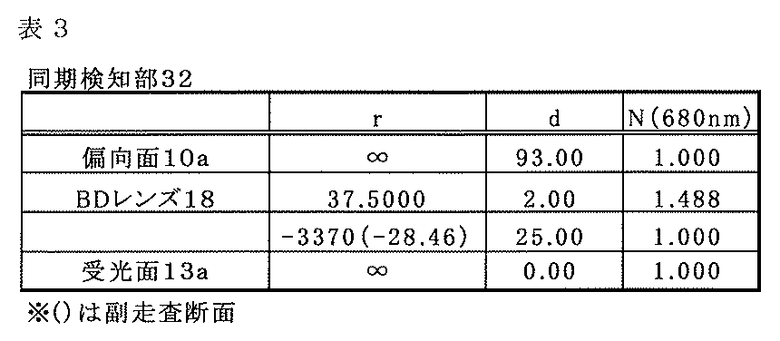
表3に、本実施例に係る同期検知部32に関する各数値を示す。
Table 3 shows numerical values related to the
BDレンズ18は、実施例1に係るBDレンズ12と同様に、樹脂から成るアナモフィックレンズであり、主走査断面内では受光面13aにピントを合わせつつ、副走査断面内では受光面13aにピントを合わせないようにしている。ただし、BDレンズ18の各レンズ面は、表3に示した曲率半径を有する基準レンズ面の一部を切り出した形状となっている。そして、各基準レンズ面の面頂点(不図示)における法線は、主走査断面内において8°の角度を成している。このように、BDレンズ18にウェッジプリズムの機能を持たせることで、同期検知部32を構成する部品点数を削減することができる。
Similar to the
本実施例では、偏向面10aからBDレンズ18までの距離LBD=93mmであり、θBD及びLsの値は実施例1と同様であるため、LBD×cosθBD=62.2<90となり、条件式(1)を満足している。また、θmaxの値も実施例1と同様であるため、条件式(2)を満足している。図5に示すように、本実施例では、BDレンズ18が配置されていない場合の光束の集光位置14に対して、5.3mm下方の位置に光束を集光させることができる。
In this embodiment, the distance L BD = 93 mm from the deflecting
以上、本実施例に係る光走査装置によれば、実施例1に係る光走査装置よりも少ない部品点数で、小型化及び高精度な同期検知を実現することができる。 As described above, according to the optical scanning device according to the present embodiment, it is possible to realize downsizing and high-precision synchronization detection with fewer parts than the optical scanning device according to the first embodiment.
[実施例3]
以下、本発明の実施例3に係る光走査装置について詳細に説明する。本実施例に係る光走査装置は、同期検知部以外については実施例1に係る光走査装置の構成と同様であるため、それについての説明を省略する。
[Example 3]
Hereinafter, an optical scanning device according to a third embodiment of the present invention will be described in detail. Since the optical scanning device according to the present embodiment is the same as the configuration of the optical scanning device according to the first embodiment except for the synchronization detection unit, description thereof will be omitted.
図6は、本実施例に係る同期検知部33の要部断面図である。本実施例に係る同期検知部33は、実施例2に係る同期検知部32と同様に、実施例1に係るウェッジプリズム11及びBDレンズ12の両方の機能を備える1つのBDレンズ19を有している。そして、BDレンズ19は、実施例2に係るBDレンズ18とは異なり、回折格子が設けられた回折面を含んでいる。
FIG. 6 is a cross-sectional view of a main part of the
表4に、本実施例に係る同期検知部33に関する各数値を示す。
Table 4 shows numerical values related to the
本実施例に係るBDレンズ19は、実施例2に係るBDレンズ18と同様に、主走査断面内において入射面及び出射面の夫々の基準レンズ面の面頂点における法線が8°の角度を成した、ウェッジプリズム状のアナモフィックレンズである。そして、本実施例でも、実施例2と同様に、条件式(1)及び(2)を満足している。図6に示すように、本実施例では、BDレンズ19が配置されていない場合の光束の集光位置14に対して、5.3mm下方の位置に光束を集光させることができる。そして、BDレンズ19の出射面は、以下の光路差関数で表されるブレーズ型の回折面である。
Similar to the BD lens 18 according to the second embodiment, the
ここで、mは回折次数、λは光源1の発振波長、E1〜E10及びF0〜F10は位相係数、である。BDレンズ19に回折面を設けることにより、倍率色収差を補正し、環境変動(温度変化)による光源1の発振波長の変化に起因する同期検知タイミングのずれを低減することができる。なお、回折面を設ける代わりに、プリズム等を用いて倍率色収差を補正することも可能であるが、その場合、部品点数の増加により各部材の配置自由度が低下してしまうため、本実施例のように回折面を採用することが望ましい。
Here, m is the diffraction order, λ is the oscillation wavelength of the light source 1, and E 1 to E 10 and F 0 to F 10 are phase coefficients. By providing the
本実施例では、回折次数m=1とし、BDレンズ19の屈折面で発生する倍率色収差を打ち消すように、回折面の位相係数が決定されている。具体的には、一次のyの係数(E1及びF1)のみを用いて回折格子を設計しており、その格子ピッチは246μmで一定となっている。これにより、回折面を形成する際の金型の加工や、回折面を金型から離型することが容易になるため、結果として回折面の製造を容易にすることができる。
In this embodiment, the diffraction order m = 1, and the phase coefficient of the diffractive surface is determined so as to cancel the lateral chromatic aberration generated on the refracting surface of the
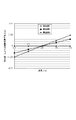
図7は、上述した各実施例に係る受光面13a上での倍率色収差を示す図である。図7において、縦軸は受光面13a上での主走査方向における結像位置ずれを示し、横軸は光源1の発振波長を示している。図7に示す通り、本実施例においては、光源1の発振波長が変化したときの結像位置ずれの発生を抑制することができている。
FIG. 7 is a diagram showing chromatic aberration of magnification on the
なお、受光面13a上での主走査方向における結像位置ずれをδY、結像光学系20及び同期検知部33の主走査断面内における焦点距離を各々f及びfBD、光走査装置100の解像度をDPI、とするとき、以下の条件式(3)を満足することが望ましい。
(f/fBD)×δY≦(25.4/DPI)/2 ・・・(3)
The imaging position shift in the main scanning direction on the
(F / f BD ) × δY ≦ (25.4 / DPI) / 2 (3)
条件式(3)の左辺は、受光面13a上での結像位置ずれδYが、被走査面17では同期検知部33の焦点距離に対する結像光学系20の焦点距離の比率に応じて拡大されるということを示している。条件式(3)を満たすことで、被走査面17での拡大された結像位置ずれを、印字解像度DPIにより決定されるドット(画素)のピッチの1/2以下に抑えることができ、良好な画像を得ることが可能になる。条件式(3)を変形すると、以下の条件式(4)が得られる。
δY≦(25.4/DPI)/2×(fBD/f) ・・・(4)
In the left side of the conditional expression (3), the imaging position deviation δY on the
δY ≦ (25.4 / DPI) / 2 × (f BD / f) (4)
本実施例では、f=250(mm)、fBD=76.8(mm)、DPI=2400(dpi)、であり、(25.4/2400)/2×(76.8/250)=1.63(μm)となる。よって、受光面13a上での結像位置ずれδYの上限値を1.63(μm)とし、それに応じて光源1の発振波長の変化の許容量を決定することが望ましい。
In this embodiment, f = 250 (mm), f BD = 76.8 (mm), DPI = 2400 (dpi), and (25.4 / 2400) / 2 × (76.8 / 250) = 1.63 (μm). Therefore, it is desirable to set the upper limit value of the imaging position deviation δY on the
このとき、図7に示したように、本実施例では、回折面を用いて同期検知部33の倍率色収差を低減しているため、実施例1や実施例2と比較して、光源1の発振波長の変化の許容量が大きくなる。これにより、発光点間の発振波長のばらつきが大きい安価なレーザーや、環境変化(温度変化)による発振波長の変化が大きい端面発光レーザーなどを、光源1として採用することが可能になる。
At this time, as shown in FIG. 7, in the present embodiment, the chromatic aberration of magnification of the
また、本実施例においては、実施例1や実施例2とは異なり、光源1における発光点LD1〜LD32から出射する全ての光束を同期検知部33により検知している。これにより、実施例1や実施例2のように、1つのBD信号に基づいて各発光点の発光タイミングを算出する必要がなくなり、かつ各発光タイミングのデータを保持するためのメモリーの容量を低減することができ、同期制御部を低コスト化することが可能になる。
Further, in the present embodiment, unlike the first and second embodiments, all the light beams emitted from the light emitting points LD1 to LD32 in the light source 1 are detected by the
以上、本実施例に係る光走査装置によれば、実施例2に係る光走査装置よりも光源1の発振波長の変化の許容量を大きくし、安価な構成で高い印字精度を実現することができる。 As described above, according to the optical scanning device according to the present embodiment, the allowable amount of the change in the oscillation wavelength of the light source 1 can be made larger than that of the optical scanning device according to the second embodiment, and high printing accuracy can be realized with an inexpensive configuration. it can.
[画像形成装置]
図8は、本発明の実施形態に係る画像形成装置80の要部概略図(ZX断面図)である。画像形成装置80は、上述した実施例1乃至3のいずれかに係る光走査装置を4つ備え、並行して4つの感光ドラム(感光体)の感光面(被走査面)に画像情報を記録する、タンデムタイプのカラー画像形成装置である。
[Image forming apparatus]
FIG. 8 is a schematic diagram (ZX cross-sectional view) of a main part of the
画像形成装置80は、プリンタコントローラ83と、光走査装置101,102,103,104と、感光ドラム201,202,203,204と、現像器301,302,303,304と、搬送ベルト81と、定着器84とを備えている。ここで、光走査装置101〜104は、副走査方向が感光ドラム201〜204の夫々の回転方向であるZ方向に一致するように配置されている。
The
図8に示すように、パーソナルコンピュータ等の外部機器82からは、R(レッド),G(グリーン),B(ブルー)の各色信号が出力される。各色信号は、プリンタコントローラ83によってY(イエロー),M(マゼンタ),C(シアン),K(ブラック)の各画像データ(ドットデータ)に変換され、光走査装置101〜104に入力される。なお、プリンタコントローラ83は、前述した信号の変換だけでなく、後述するモータなどの画像形成装置80における各部の制御を行う。
As shown in FIG. 8, R (red), G (green), and B (blue) color signals are output from an
光走査装置101〜104の夫々は、各画像データに応じて変調された光束401,402,403,404の夫々によって、像担持体としての感光ドラム201〜204の感光面を主走査方向(Y方向)に光走査する。感光ドラム201〜204の夫々は、不図示のモータによって時計回りに回転させられ、この回転に伴って各感光面が光束401〜404に対して副走査方向(Z方向)に移動する。光束401〜404の夫々により、不図示の帯電ローラにより帯電させられた各感光面が露光されることで、各感光面上に静電潜像が形成される。
Each of the
その後、感光ドラム201〜204の各感光面上に形成された各色の静電潜像は、現像器301〜304の夫々によって各色のトナー像として現像される。そして、各色のトナー像は、不図示の転写器によって、搬送ベルト81により搬送されてきた被転写材に多重転写された後、定着器84によって定着させられる。以上の工程により、1枚のフルカラー画像が形成される。
Thereafter, the electrostatic latent images of the respective colors formed on the photosensitive surfaces of the
なお、画像形成装置80は、実施例1乃至3で示したような、1つの偏向器により1つの被走査面を光走査する光走査装置を4つ備える構成を採用しているが、これに限られるものではない。例えば、1つの偏向器により4つの被走査面を光走査する光走査装置を1つ備える構成や、1つの偏向器により2つの被走査面を光走査する光走査装置を2つ備える構成などを採用してもよい。また、例えばCCDセンサーやCMOSセンサー等のラインセンサーを備えたカラー画像読取装置を、外部機器82として画像形成装置80に接続することにより、カラーデジタル複写機を構成してもよい。
The
[変形例]
以上、本発明の好ましい実施形態及び実施例について説明したが、本発明はこれらの実施形態及び実施例に限定されず、その要旨の範囲内で種々の組合せ、変形及び変更が可能である。
[Modification]
The preferred embodiments and examples of the present invention have been described above, but the present invention is not limited to these embodiments and examples, and various combinations, modifications, and changes can be made within the scope of the gist.
例えば、各実施例においては、1つの光源からの光束により1つの被走査面を光走査しているが、これに限らず、複数の光源からの光束により複数の被走査面を光走査する構成を採用してもよい。このとき、偏向器の複数の偏向面により複数の光束を同時に偏向する構成を採ってもよい。そして、偏向面から複数の被走査面に至る夫々の光路において、結像レンズを個別に配置してもよいし、結像レンズを一体化して光路同士で共有するように構成してもよい。なお、結像レンズの数、材料、及び形状については、光走査装置の構成に応じて適宜変更してもよい。 For example, in each embodiment, one scanned surface is optically scanned with a light beam from one light source. However, the present invention is not limited thereto, and a plurality of scanned surfaces are optically scanned with light beams from a plurality of light sources. May be adopted. At this time, a configuration in which a plurality of light beams are simultaneously deflected by a plurality of deflection surfaces of the deflector may be employed. In each optical path from the deflection surface to the plurality of scanned surfaces, the imaging lenses may be individually arranged, or the imaging lenses may be integrated and shared by the optical paths. Note that the number, material, and shape of the imaging lens may be appropriately changed according to the configuration of the optical scanning device.
また、図1で示したように、各実施例に係る同期検知部は、結像光学系の光軸に対して光源と同じ側(結像光学系よりも走査上流側)に配置されているが、必要に応じて光源とは反対側(結像光学系よりも走査下流側)に配置してもよい。ただし、偏向器により偏向された光束が結像光学系に入射する直前、すなわち被走査面上での書き出しの直前に同期検知を行った方が、検知誤差を小さくすることができるため、結像光学系よりも走査上流側に同期検知部を配置することがより好ましい。 As shown in FIG. 1, the synchronization detection unit according to each embodiment is disposed on the same side as the light source with respect to the optical axis of the imaging optical system (scanning upstream side of the imaging optical system). However, it may be arranged on the side opposite to the light source (on the downstream side of the imaging optical system) as necessary. However, since the detection error can be reduced if synchronous detection is performed immediately before the light beam deflected by the deflector enters the imaging optical system, that is, immediately before writing on the scanning surface, imaging is performed. More preferably, the synchronization detection unit is disposed upstream of the optical system.
そして、各実施例において、同期検知部からのBD信号に基づいて光源の発光タイミングを制御する同期制御部は、光走査装置の内部に配置されていてもよいし、光走査装置の外部かつ画像形成装置の内部に配置されていてもよい。また、光量検知部と同期検知部とで制御部を共有し、1つの制御部により光量制御及び光源の発光タイミングの制御の両方を行うように構成してもよい。 In each of the embodiments, the synchronization control unit that controls the light emission timing of the light source based on the BD signal from the synchronization detection unit may be arranged inside the optical scanning device, or outside the optical scanning device and in the image. It may be arranged inside the forming apparatus. In addition, the control unit may be shared by the light amount detection unit and the synchronization detection unit, and both the light amount control and the light emission timing control of the light source may be performed by one control unit.
なお、実施例1においては、入射光学系40におけるプリズム7及び同期検知部30のウェッジプリズム11として、同一の形状のものを採用しているが、必要に応じて互いに異なる形状のものを採用してもよい。例えば、実施例1ではウェッジプリズム11の各光学面を平面としているが、必要に応じて各光学面にパワーを持たせてもよい。ただし、同一の金型を用いることを可能にし、製造を容易にするためには、各プリズムとして同一の形状のものを採用することが好ましく、各光学面を平面とすることがより好ましい。
In the first embodiment, the prism 7 in the incident
さらに、実施例1に係るウェッジプリズム11やBDレンズ12の各光学面のうちの少なくとも1つを、実施例3と同様に回折面としてもよい。また、BDレンズ12を偏心させる際は、シフト偏心のみに限らず、シフト偏心及び/又はチルト偏心させてもよい。そして、同期検知部30におけるウェッジプリズム11の位置は、上記条件式(1)を満たしていればよく、必要に応じてBDレンズ12の位置と入れ替えてもよい。なお、偏向器10から同期検知部30に至る光路には、ミラー等の反射光学素子が配置されていなければよく、必要に応じて他の屈折光学素子を設けてもよい。
Furthermore, at least one of the optical surfaces of the wedge prism 11 and the
10 偏向器
11 屈折光学素子
13 受光部
17 被走査面
20 結像光学系
100 光走査装置
DESCRIPTION OF
Claims (21)
該偏向器により偏向された光束を前記被走査面に導光する結像光学系と、
前記偏向器により偏向された光束を受光して信号を生成する受光部と、
前記偏向器により偏向された光束の主光線を、主走査断面内において前記結像光学系から離れる方向に屈折させて、前記受光部の受光面に導光する屈折光学素子と、を備え、
主走査断面内において、前記偏向器の偏向面から前記屈折光学素子の入射面までの距離をLBD、前記受光面の中心に向かうときの前記屈折光学素子に入射する光束の主光線と前記結像光学系の光軸との成す角度をθBD、前記偏向面から前記結像光学系の最も前記偏向面に近い光学面までの距離をLs、とするとき、
LBD×cosθBD≦Ls
なる条件を満足することを特徴とする光走査装置。 A deflector that deflects a light beam and optically scans the surface to be scanned in the main scanning direction;
An imaging optical system for guiding the light beam deflected by the deflector to the surface to be scanned;
A light receiving unit that receives a light beam deflected by the deflector and generates a signal;
A refracting optical element that refracts the principal ray of the light beam deflected by the deflector in a direction away from the imaging optical system in a main scanning section and guides it to the light receiving surface of the light receiving unit;
In the main scanning section, the distance from the deflecting surface of the deflector to the incident surface of the refractive optical element is L BD , and the principal ray of the light beam incident on the refractive optical element when traveling toward the center of the light receiving surface and the concatenation. When the angle formed by the optical axis of the image optical system is θ BD , and the distance from the deflection surface to the optical surface closest to the deflection surface of the imaging optical system is Ls,
L BD × cos θ BD ≦ Ls
An optical scanning device characterized by satisfying the following conditions.
1.1<θBD/θmax<1.5
なる条件を満足することを特徴とする請求項1に記載の光走査装置。 When the maximum scanning field angle of the deflector corresponding to the effective scanning area on the scanned surface is θ max ,
1.1 <θ BD / θ max <1.5
The optical scanning device according to claim 1, wherein the following condition is satisfied.
θs<θBD<(θi−θs)/2
なる条件を満足することを特徴とする請求項14乃至17の何れか1項に記載の光走査装置。 The angle formed between the principal ray of the light beam incident on the end of the optical surface closest to the deflection surface of the imaging optical system on the light receiving portion side and the optical axis of the imaging optical system is θ s . When the angle formed by the optical axis of the image optical system and the optical axis of the incident optical system is θ i ,
θ s <θ BD <(θ i −θ s ) / 2
The optical scanning device according to claim 14, wherein the following condition is satisfied.
Priority Applications (1)
| Application Number | Priority Date | Filing Date | Title |
|---|---|---|---|
| JP2016079045A JP2017191143A (en) | 2016-04-11 | 2016-04-11 | Optical scanner and image forming apparatus including the same |
Applications Claiming Priority (1)
| Application Number | Priority Date | Filing Date | Title |
|---|---|---|---|
| JP2016079045A JP2017191143A (en) | 2016-04-11 | 2016-04-11 | Optical scanner and image forming apparatus including the same |
Publications (1)
| Publication Number | Publication Date |
|---|---|
| JP2017191143A true JP2017191143A (en) | 2017-10-19 |
Family
ID=60086199
Family Applications (1)
| Application Number | Title | Priority Date | Filing Date |
|---|---|---|---|
| JP2016079045A Pending JP2017191143A (en) | 2016-04-11 | 2016-04-11 | Optical scanner and image forming apparatus including the same |
Country Status (1)
| Country | Link |
|---|---|
| JP (1) | JP2017191143A (en) |
Cited By (1)
| Publication number | Priority date | Publication date | Assignee | Title |
|---|---|---|---|---|
| WO2023162380A1 (en) * | 2022-02-28 | 2023-08-31 | キヤノン株式会社 | Reflective element, light detection device, and optical scanning device |
-
2016
- 2016-04-11 JP JP2016079045A patent/JP2017191143A/en active Pending
Cited By (1)
| Publication number | Priority date | Publication date | Assignee | Title |
|---|---|---|---|---|
| WO2023162380A1 (en) * | 2022-02-28 | 2023-08-31 | キヤノン株式会社 | Reflective element, light detection device, and optical scanning device |
Similar Documents
| Publication | Publication Date | Title |
|---|---|---|
| US7956884B2 (en) | Optical scanning device and image forming apparatus | |
| JP5137428B2 (en) | Optical scanning device and image forming apparatus using the same | |
| US7929007B2 (en) | Optical scanning device and image forming apparatus | |
| US8699077B2 (en) | Scanning optical apparatus and image forming apparatus using the same | |
| JP2004070107A (en) | Optical scanning device and image forming apparatus using the same | |
| US8705158B2 (en) | Scanning optical device and image forming apparatus using the same | |
| US8314824B2 (en) | Optical scanning apparatus and image forming apparatus using the same | |
| JP4250572B2 (en) | Optical scanning device and image forming apparatus using the same | |
| JP5882692B2 (en) | Optical scanning apparatus and image forming apparatus | |
| JP6021407B2 (en) | Optical scanning device and image forming apparatus having the same | |
| US20020050562A1 (en) | Light scanner and image forming apparatus using the same | |
| JP2000019441A (en) | Image forming device | |
| JP2010072050A (en) | Optical scanner and method of adjusting optical scanner | |
| JP6132701B2 (en) | Optical scanning device and image forming apparatus using the same | |
| JP6425752B2 (en) | Optical scanning device and image forming apparatus provided with the same | |
| US20050098716A1 (en) | Light scanner and image forming apparatus using the same | |
| JP2008304607A (en) | Optical scanning device and image forming apparatus using the same | |
| JP6234085B2 (en) | Optical scanning device and image forming apparatus using the same | |
| JP2016194675A (en) | Optical scanner | |
| JP4404667B2 (en) | Optical scanning device | |
| JP4401950B2 (en) | Optical scanning device and image forming apparatus using the same | |
| JP4902279B2 (en) | Image forming apparatus | |
| JP7581103B2 (en) | Optical scanning device and image forming device | |
| JP6667274B2 (en) | Optical scanning device, image forming apparatus, and imaging optical element | |
| JP2019095647A (en) | Optical scanner and image forming apparatus including the same |