JP2017191594A - サニタイズ認識dramコントローラ - Google Patents
サニタイズ認識dramコントローラ Download PDFInfo
- Publication number
- JP2017191594A JP2017191594A JP2016249420A JP2016249420A JP2017191594A JP 2017191594 A JP2017191594 A JP 2017191594A JP 2016249420 A JP2016249420 A JP 2016249420A JP 2016249420 A JP2016249420 A JP 2016249420A JP 2017191594 A JP2017191594 A JP 2017191594A
- Authority
- JP
- Japan
- Prior art keywords
- block
- dram
- controller
- flag
- blocks
- Prior art date
- Legal status (The legal status is an assumption and is not a legal conclusion. Google has not performed a legal analysis and makes no representation as to the accuracy of the status listed.)
- Granted
Links
Images


Classifications
-
- G—PHYSICS
- G11—INFORMATION STORAGE
- G11C—STATIC STORES
- G11C11/00—Digital stores characterised by the use of particular electric or magnetic storage elements; Storage elements therefor
- G11C11/21—Digital stores characterised by the use of particular electric or magnetic storage elements; Storage elements therefor using electric elements
- G11C11/34—Digital stores characterised by the use of particular electric or magnetic storage elements; Storage elements therefor using electric elements using semiconductor devices
- G11C11/40—Digital stores characterised by the use of particular electric or magnetic storage elements; Storage elements therefor using electric elements using semiconductor devices using transistors
- G11C11/401—Digital stores characterised by the use of particular electric or magnetic storage elements; Storage elements therefor using electric elements using semiconductor devices using transistors forming cells needing refreshing or charge regeneration, i.e. dynamic cells
- G11C11/406—Management or control of the refreshing or charge-regeneration cycles
-
- G—PHYSICS
- G06—COMPUTING OR CALCULATING; COUNTING
- G06F—ELECTRIC DIGITAL DATA PROCESSING
- G06F13/00—Interconnection of, or transfer of information or other signals between, memories, input/output devices or central processing units
- G06F13/14—Handling requests for interconnection or transfer
- G06F13/16—Handling requests for interconnection or transfer for access to memory bus
- G06F13/1605—Handling requests for interconnection or transfer for access to memory bus based on arbitration
- G06F13/161—Handling requests for interconnection or transfer for access to memory bus based on arbitration with latency improvement
- G06F13/1636—Handling requests for interconnection or transfer for access to memory bus based on arbitration with latency improvement using refresh
-
- G—PHYSICS
- G06—COMPUTING OR CALCULATING; COUNTING
- G06F—ELECTRIC DIGITAL DATA PROCESSING
- G06F12/00—Accessing, addressing or allocating within memory systems or architectures
- G06F12/02—Addressing or allocation; Relocation
- G06F12/08—Addressing or allocation; Relocation in hierarchically structured memory systems, e.g. virtual memory systems
- G06F12/0802—Addressing of a memory level in which the access to the desired data or data block requires associative addressing means, e.g. caches
- G06F12/0893—Caches characterised by their organisation or structure
-
- G—PHYSICS
- G06—COMPUTING OR CALCULATING; COUNTING
- G06F—ELECTRIC DIGITAL DATA PROCESSING
- G06F12/00—Accessing, addressing or allocating within memory systems or architectures
- G06F12/14—Protection against unauthorised use of memory or access to memory
-
- G—PHYSICS
- G06—COMPUTING OR CALCULATING; COUNTING
- G06F—ELECTRIC DIGITAL DATA PROCESSING
- G06F3/00—Input arrangements for transferring data to be processed into a form capable of being handled by the computer; Output arrangements for transferring data from processing unit to output unit, e.g. interface arrangements
- G06F3/06—Digital input from, or digital output to, record carriers, e.g. RAID, emulated record carriers or networked record carriers
- G06F3/0601—Interfaces specially adapted for storage systems
- G06F3/0602—Interfaces specially adapted for storage systems specifically adapted to achieve a particular effect
- G06F3/0614—Improving the reliability of storage systems
- G06F3/0619—Improving the reliability of storage systems in relation to data integrity, e.g. data losses, bit errors
-
- G—PHYSICS
- G06—COMPUTING OR CALCULATING; COUNTING
- G06F—ELECTRIC DIGITAL DATA PROCESSING
- G06F3/00—Input arrangements for transferring data to be processed into a form capable of being handled by the computer; Output arrangements for transferring data from processing unit to output unit, e.g. interface arrangements
- G06F3/06—Digital input from, or digital output to, record carriers, e.g. RAID, emulated record carriers or networked record carriers
- G06F3/0601—Interfaces specially adapted for storage systems
- G06F3/0628—Interfaces specially adapted for storage systems making use of a particular technique
- G06F3/0638—Organizing or formatting or addressing of data
- G06F3/064—Management of blocks
-
- G—PHYSICS
- G06—COMPUTING OR CALCULATING; COUNTING
- G06F—ELECTRIC DIGITAL DATA PROCESSING
- G06F3/00—Input arrangements for transferring data to be processed into a form capable of being handled by the computer; Output arrangements for transferring data from processing unit to output unit, e.g. interface arrangements
- G06F3/06—Digital input from, or digital output to, record carriers, e.g. RAID, emulated record carriers or networked record carriers
- G06F3/0601—Interfaces specially adapted for storage systems
- G06F3/0628—Interfaces specially adapted for storage systems making use of a particular technique
- G06F3/0655—Vertical data movement, i.e. input-output transfer; data movement between one or more hosts and one or more storage devices
- G06F3/0659—Command handling arrangements, e.g. command buffers, queues, command scheduling
-
- G—PHYSICS
- G06—COMPUTING OR CALCULATING; COUNTING
- G06F—ELECTRIC DIGITAL DATA PROCESSING
- G06F3/00—Input arrangements for transferring data to be processed into a form capable of being handled by the computer; Output arrangements for transferring data from processing unit to output unit, e.g. interface arrangements
- G06F3/06—Digital input from, or digital output to, record carriers, e.g. RAID, emulated record carriers or networked record carriers
- G06F3/0601—Interfaces specially adapted for storage systems
- G06F3/0668—Interfaces specially adapted for storage systems adopting a particular infrastructure
- G06F3/0671—In-line storage system
- G06F3/0673—Single storage device
-
- G—PHYSICS
- G11—INFORMATION STORAGE
- G11C—STATIC STORES
- G11C11/00—Digital stores characterised by the use of particular electric or magnetic storage elements; Storage elements therefor
- G11C11/21—Digital stores characterised by the use of particular electric or magnetic storage elements; Storage elements therefor using electric elements
- G11C11/34—Digital stores characterised by the use of particular electric or magnetic storage elements; Storage elements therefor using electric elements using semiconductor devices
- G11C11/40—Digital stores characterised by the use of particular electric or magnetic storage elements; Storage elements therefor using electric elements using semiconductor devices using transistors
- G11C11/401—Digital stores characterised by the use of particular electric or magnetic storage elements; Storage elements therefor using electric elements using semiconductor devices using transistors forming cells needing refreshing or charge regeneration, i.e. dynamic cells
- G11C11/406—Management or control of the refreshing or charge-regeneration cycles
- G11C11/40622—Partial refresh of memory arrays
-
- G—PHYSICS
- G11—INFORMATION STORAGE
- G11C—STATIC STORES
- G11C11/00—Digital stores characterised by the use of particular electric or magnetic storage elements; Storage elements therefor
- G11C11/21—Digital stores characterised by the use of particular electric or magnetic storage elements; Storage elements therefor using electric elements
- G11C11/34—Digital stores characterised by the use of particular electric or magnetic storage elements; Storage elements therefor using electric elements using semiconductor devices
- G11C11/40—Digital stores characterised by the use of particular electric or magnetic storage elements; Storage elements therefor using electric elements using semiconductor devices using transistors
- G11C11/401—Digital stores characterised by the use of particular electric or magnetic storage elements; Storage elements therefor using electric elements using semiconductor devices using transistors forming cells needing refreshing or charge regeneration, i.e. dynamic cells
- G11C11/4063—Auxiliary circuits, e.g. for addressing, decoding, driving, writing, sensing or timing
- G11C11/407—Auxiliary circuits, e.g. for addressing, decoding, driving, writing, sensing or timing for memory cells of the field-effect type
- G11C11/409—Read-write [R-W] circuits
-
- G—PHYSICS
- G06—COMPUTING OR CALCULATING; COUNTING
- G06F—ELECTRIC DIGITAL DATA PROCESSING
- G06F2212/00—Indexing scheme relating to accessing, addressing or allocation within memory systems or architectures
- G06F2212/10—Providing a specific technical effect
- G06F2212/1028—Power efficiency
-
- G—PHYSICS
- G06—COMPUTING OR CALCULATING; COUNTING
- G06F—ELECTRIC DIGITAL DATA PROCESSING
- G06F2212/00—Indexing scheme relating to accessing, addressing or allocation within memory systems or architectures
- G06F2212/10—Providing a specific technical effect
- G06F2212/1052—Security improvement
-
- G—PHYSICS
- G11—INFORMATION STORAGE
- G11C—STATIC STORES
- G11C11/00—Digital stores characterised by the use of particular electric or magnetic storage elements; Storage elements therefor
- G11C11/21—Digital stores characterised by the use of particular electric or magnetic storage elements; Storage elements therefor using electric elements
- G11C11/34—Digital stores characterised by the use of particular electric or magnetic storage elements; Storage elements therefor using electric elements using semiconductor devices
- G11C11/40—Digital stores characterised by the use of particular electric or magnetic storage elements; Storage elements therefor using electric elements using semiconductor devices using transistors
- G11C11/401—Digital stores characterised by the use of particular electric or magnetic storage elements; Storage elements therefor using electric elements using semiconductor devices using transistors forming cells needing refreshing or charge regeneration, i.e. dynamic cells
- G11C11/406—Management or control of the refreshing or charge-regeneration cycles
- G11C11/40611—External triggering or timing of internal or partially internal refresh operations, e.g. auto-refresh or CAS-before-RAS triggered refresh
-
- Y—GENERAL TAGGING OF NEW TECHNOLOGICAL DEVELOPMENTS; GENERAL TAGGING OF CROSS-SECTIONAL TECHNOLOGIES SPANNING OVER SEVERAL SECTIONS OF THE IPC; TECHNICAL SUBJECTS COVERED BY FORMER USPC CROSS-REFERENCE ART COLLECTIONS [XRACs] AND DIGESTS
- Y02—TECHNOLOGIES OR APPLICATIONS FOR MITIGATION OR ADAPTATION AGAINST CLIMATE CHANGE
- Y02D—CLIMATE CHANGE MITIGATION TECHNOLOGIES IN INFORMATION AND COMMUNICATION TECHNOLOGIES [ICT], I.E. INFORMATION AND COMMUNICATION TECHNOLOGIES AIMING AT THE REDUCTION OF THEIR OWN ENERGY USE
- Y02D10/00—Energy efficient computing, e.g. low power processors, power management or thermal management
Landscapes
- Engineering & Computer Science (AREA)
- Theoretical Computer Science (AREA)
- Physics & Mathematics (AREA)
- General Engineering & Computer Science (AREA)
- General Physics & Mathematics (AREA)
- Computer Hardware Design (AREA)
- Microelectronics & Electronic Packaging (AREA)
- Human Computer Interaction (AREA)
- Computer Security & Cryptography (AREA)
- Dram (AREA)
- Memory System (AREA)
- Read Only Memory (AREA)
- Storage Device Security (AREA)
- Techniques For Improving Reliability Of Storages (AREA)
Abstract
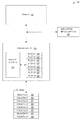
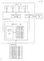
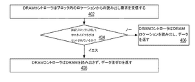
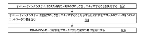
【解決手段】DRAMコントローラは、それぞれがDRAMの複数のブロックのうちの1つのブロックとの関連付けのための複数のフラグを含む。サニタイズコントローラは、1つのブロックがサニタイズされるべきであると判定し、それに応答して複数のブロックのうちの1つのブロックと関連する1つのフラグをセットし、該ブロックのリフレッシュをディセーブルする。引き続くブロック内のロケーションからのデータ読み取り要求の受信に応答して、フラグがクリアされていない場合には、DRAMコントローラはロケーションを読み出し、そこから読み出されたデータを返す。フラグがセットされている場合には、DRAMコントローラはDRAMの読み出しを行わず、ゼロの値を返さない。
【選択図】図4
Description
本出願は、参照によりその全体が本明細書に組み込まれる、SANITIZE−AWARE DRAM CONTROLLERと題する米国仮出願第62/323,177号(2006年4月15日出願)に基づく優先権を主張する。
Claims (20)
- 複数のブロックを含むダイナミック・ランダム・アクセス・メモリ(DRAM)を制御するためのDRAMコントローラであって、ブロックは前記DRAM内の1つ又は複数のストレージ・ユニットであり、当該DRAMコントローラは前記DRAMに対するリフレッシュを選択的にイネーブル又はディセーブルすることができ、
当該DRAMコントローラは、
それぞれが前記DRAMの複数のブロックのうちの1つのブロックと関連する複数のフラグと、
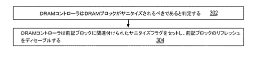
前記複数のブロックのうちの1つのブロックがサニタイズされるべきであると判定し、それに応答して前記複数のブロックのうちの1つのブロックと関連する、前記複数のフラグのうちの1つのフラグをセットし、該ブロックのリフレッシュをディセーブルするサニタイズコントローラと、を含み、
引き続く前記ブロック内のロケーションからのデータ読み取り要求の受信に応答して、前記フラグがクリアされている場合には、当該DRAMコントローラは前記ロケーションを読み出し、そこから読み出されたデータを返し、前記フラグがセットされている場合には、当該DRAMコントローラはゼロ値を返し、DRAMの読み出しを行わない、DRAMコントローラ。 - 引き続く前記ブロック内のロケーションへのデータ書き込み要求の受信に応答して、
(a)前記フラグがクリアされている場合には、当該DRAMコントローラは前記データを前記ロケーションに書き込み、
(b)前記フラグがセットされている場合には、当該DRAMコントローラは前記ブロックのリフレッシュをイネーブルし、前記データを前記ロケーションへ書き込むことをさらに含む、請求項1記載のDRAMコントローラ。 - 引き続く前記ブロック内の前記ロケーションへのデータ書き込み要求の受信に応答して、
(b)前記フラグがセットされている場合には、当該DRAMコントローラはさらに前記フラグをクリアし、前記ブロック内の全ての他のロケーションにゼロ値を書き込むことをさらに含む、請求項2記載のDRAMコントローラ。 - 引き続く前記ブロック内の前記ロケーションへのデータ書き込み要求の受信に応答して、
前記フラグがセットされている場合には、当該DRAMコントローラは、書き込まれるべきデータが非ゼロである場合にのみ、動作(a)及び(b)を実行することをさらに含む、請求項2記載のDRAMコントローラ。 - コントロールレジスタをさらに含み、
前記サニタイズコントローラは、前記DRAM及び当該DRAMコントローラを含むシステムのシステムソフトウェアにより前記コントロールレジスタへの書き込みを検出することによって、前記ブロックがサニタイズされるべきであると判定する、請求項1に記載のDRAMコントローラ。 - 前記サニタイズコントローラは、前記ブロックの全てのロケーションへ、前記ブロックのロケーションへの非ゼロ値の書き込みの介入なしに、一連のゼロ値書き込みを検出することによって、前記ブロックがサニタイズされるべきであると判断するハードウェアをさらに備える、請求項1に記載のDRAMコントローラ。
- 前記ハードウェアは、
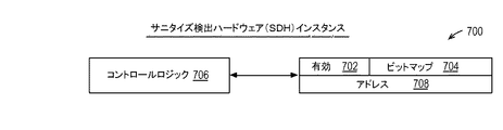
前記DRAMの前記複数のブロックの異なるブロックに対し、前記サニタイズコントローラによって別個に割り当て可能な複数のサニタイズ検出ハードウェアインスタンスを含む、請求項6記載のDRAMコントローラ。 - 各サニタイズ検出ハードウェアインスタンスは、
DRAMコントローラがブロック内のどのロケーションにゼロ値が書き込まれたかを追跡するために使用するビットマップと、
前記ビットマップが全て真のビットを有するときを検出するロジックとを備える、請求項7に記載のDRAMコントローラ。 - 各サニタイズ検出ハードウェアインスタンスは、
最も新しくゼロ値が書き込まれた前記ブロック内の固定サイズのワードの後の次の固定長のワードのインデックスを保持するレジスタであって、当該インデックスが現在のゼロ値の固定長ワード書き込みのインデックスと一致するとインクリメントされるレジスタと、
前記現在のゼロ値の固定長ワード書き込みのインデックスが前記ブロック内の最高インデックスとなるときを検出するロジックとを備える、請求項7に記載のDRAMコントローラ。 - 複数のブロックを含むダイナミック・ランダム・アクセス・メモリ(DRAM)を制御するための方法であって、ブロックは前記DRAM内の1つ又は複数のストレージ・ユニットであり、DRAMコントローラは前記DRAMに対するリフレッシュを選択的にイネーブル又はディセーブルすることができ、
当該方法は、
前記複数のブロックのうちの1つのブロックがサニタイズされるべきであると判定するステップであり、それに応答して、前記複数のブロックのうちの1つのブロックと関連するフラグをセットし、該ブロックのリフレッシュをディセーブルする、判定ステップを備え、
前記フラグは、それぞれがDRAMの複数のブロックのうちの1つのブロックと関連する複数のフラグのうちの1つのフラグであり、
当該方法はさらに、
引き続く前記ブロック内のロケーションからのデータ読み取り要求の受信に応答して、
前記フラグがクリアされている場合に、前記ロケーションを読み出し、そこから読み取られたデータを返すステップと、
前記フラグがセットされている場合に、前記DRAMの読み出しを行わず、ゼロ値を返すステップと、を備える方法。 - 引き続く前記ブロック内のロケーションからのデータ読み取り要求の受信に応答して、
(a)前記フラグがクリアされている場合に、前記データを前記ロケーションに書き込むステップと、
(b)前記フラグがセットされている場合に、前記ブロックのリフレッシュをイネーブルし、前記ロケーションに前記データを書き込むステップと、をさらに備える、請求項10に記載の方法。 - 引き続く前記ブロック内のロケーションからのデータ読み取り要求の受信に応答して、
(b)前記フラグがセットされている場合に、さらに、前記フラグをクリアし、前記ブロック内の全ての他のロケーションにゼロ値を書き込むステップをさらに備える、請求項11に記載の方法。 - 引き続く前記ブロック内のロケーションからのデータ読み取り要求の受信に応答して、
前記フラグがセットされている場合に、書き込まれるべきデータが非ゼロである場合にのみ、動作(a)及び(b)を実行するステップをさらに備える、請求項11に記載の方法。 - 前記ブロックがサニタイズされるべきであると判定する前記判定ステップは、前記DRAM及びコントロールレジスタを含むDRAMコントローラを有するシステムのシステムソフトウェアによって前記コントロールレジスタへの書き込みを検出するステップをさらに備える、請求項10に記載の方法。
- 前記ブロックがサニタイズされるべきであると判定する前記判定ステップは、前記ブロックのロケーションへの非ゼロ値の書き込みの介入なしに、前記ブロックの全てのロケーションへの一連のゼロ値書き込みを検出するステップをさらに備える、請求項10に記載の方法。
- 当該方法は、前記DRAMの前記複数のブロックの異なるブロックに対し、別個に割り当て可能な複数のサニタイズ検出ハードウェアインスタンスを備えたDRAMコントローラによって実行されることをさらに含む、請求項15に記載の方法。
- 前記ブロック内のロケーションへのゼロ値の書き込みの検出に応答してビットマップのビットを真にセットするステップであって、前記ビットマップの各ビットが前記ブロック内の異なるロケーションと関連しているステップをさらに備え、
前記ブロックがサニタイズされるべきであると判定する判定ステップは、前記ビットマップが全て真のビットを有することを検出するステップをさらに備える、請求項16に記載の方法。 - インデックスが現在のゼロ値の固定長ワード書き込みのインデックスと一致すると、レジスタをインクリメントすることによって、前記ブロック内の最も新しくゼロ値が書き込まれた固定サイズのワードの後の次の固定長ワードのインデックスを保持するようにレジスタを維持するステップをさらに備え、
前記ブロックがサニタイズされるべきであると判定する前記判定ステップは、前記現在のゼロ値の固定長ワード書き込みのインデックスが前記ブロック内の最高インデックスとなるときを検出するステップを備える、請求項16に記載の方法。 - コンピューティングデバイスと共に使用するための少なくとも1つの非揮発性コンピュータ使用可能媒体において符号化されたコンピュータプログラムであって、
当該コンピュータプログラムは、
複数のブロックを含むダイナミック・ランダム・アクセス・メモリ(DRAM)を制御するためのコントローラを指定するための前記媒体内に具現化されたコンピュータ使用可能プログラムコードを含み、ブロックは前記DRAM内の1つ又は複数のストレージ・ユニットであり、DRAMコントローラは前記DRAMに対するリフレッシュを選択的にイネーブル又はディセーブルすることができ、
前記コンピュータ使用可能プログラムコードは、
それぞれが前記DRAMの複数のブロックのうちの1つのブロックと関連する複数のフラグを指定する第1のプログラムコードと、
前記複数のブロックのうちの1つのブロックがサニタイズされるべきであると判定し、それに応答して前記複数のブロックのうちの1つのブロックと関連する、前記複数のフラグのうちの1つのフラグをセットし、該ブロックのリフレッシュをディセーブルするサニタイズコントローラを指定する第2のプログラムコードとを備え、
引き続く前記ブロック内のロケーションからのデータ読み取り要求の受信に応答して、前記フラグがクリアされている場合に、当該DRAMコントローラは前記ロケーションを読み出し、そこから読み出されたデータを返し、前記フラグがセットされている場合に、当該DRAMコントローラはDRAMの読み出しを行わず、ゼロ値を返す、コンピュータプログラム。 - 前記少なくとも1つの非揮発性コンピュータ使用可能媒体は、ディスク、テープ、又は他の磁気、光学、又は電子記憶媒体の群から選択される、請求項19に記載のコンピュータプログラム。
Applications Claiming Priority (4)
| Application Number | Priority Date | Filing Date | Title |
|---|---|---|---|
| US201662323177P | 2016-04-15 | 2016-04-15 | |
| US62/323,177 | 2016-04-15 | ||
| US15/335,141 | 2016-10-26 | ||
| US15/335,141 US9972375B2 (en) | 2016-04-15 | 2016-10-26 | Sanitize-aware DRAM controller |
Publications (2)
| Publication Number | Publication Date |
|---|---|
| JP2017191594A true JP2017191594A (ja) | 2017-10-19 |
| JP6373336B2 JP6373336B2 (ja) | 2018-08-15 |
Family
ID=57838118
Family Applications (1)
| Application Number | Title | Priority Date | Filing Date |
|---|---|---|---|
| JP2016249420A Active JP6373336B2 (ja) | 2016-04-15 | 2016-12-22 | サニタイズ認識dramコントローラ |
Country Status (5)
| Country | Link |
|---|---|
| US (1) | US9972375B2 (ja) |
| EP (1) | EP3232330B1 (ja) |
| JP (1) | JP6373336B2 (ja) |
| KR (1) | KR101902650B1 (ja) |
| CN (1) | CN106782642B (ja) |
Cited By (1)
| Publication number | Priority date | Publication date | Assignee | Title |
|---|---|---|---|---|
| US20250355579A1 (en) * | 2024-05-17 | 2025-11-20 | Samsung Electronics Co., Ltd. | Storage controller performing partial refresh operation, storage device including the same, and method of operating the same |
Families Citing this family (18)
| Publication number | Priority date | Publication date | Assignee | Title |
|---|---|---|---|---|
| US10698732B2 (en) * | 2016-07-19 | 2020-06-30 | Sap Se | Page ranking in operating system virtual pages in hybrid memory systems |
| US10474557B2 (en) | 2016-07-19 | 2019-11-12 | Sap Se | Source code profiling for line-level latency and energy consumption estimation |
| US10783146B2 (en) | 2016-07-19 | 2020-09-22 | Sap Se | Join operations in hybrid main memory systems |
| US10452539B2 (en) | 2016-07-19 | 2019-10-22 | Sap Se | Simulator for enterprise-scale simulations on hybrid main memory systems |
| US10437798B2 (en) | 2016-07-19 | 2019-10-08 | Sap Se | Full system simulator and memory-aware splay tree for in-memory databases in hybrid memory systems |
| US11977484B2 (en) | 2016-07-19 | 2024-05-07 | Sap Se | Adapting in-memory database in hybrid memory systems and operating system interface |
| US10387127B2 (en) | 2016-07-19 | 2019-08-20 | Sap Se | Detecting sequential access data and random access data for placement on hybrid main memory for in-memory databases |
| US10540098B2 (en) | 2016-07-19 | 2020-01-21 | Sap Se | Workload-aware page management for in-memory databases in hybrid main memory systems |
| US10185509B1 (en) | 2017-06-01 | 2019-01-22 | Amazon Technologies, Inc. | Secure storage device sanitization |
| US11010379B2 (en) | 2017-08-15 | 2021-05-18 | Sap Se | Increasing performance of in-memory databases using re-ordered query execution plans |
| US11182106B2 (en) * | 2018-03-21 | 2021-11-23 | Arm Limited | Refresh circuit for use with integrated circuits |
| US11143684B2 (en) | 2019-03-25 | 2021-10-12 | Lg Energy Solution, Ltd. | Diagnostic system for a vehicle electrical system |
| US10996279B2 (en) | 2019-04-08 | 2021-05-04 | Lg Chem, Ltd. | Diagnostic system for a battery management system |
| US11221949B2 (en) * | 2020-02-10 | 2022-01-11 | Micron Technology, Inc. | Multi state purgatory for media management for a memory subsystem |
| US11442654B2 (en) * | 2020-10-15 | 2022-09-13 | Microsoft Technology Licensing, Llc | Managing and ranking memory resources |
| KR102825952B1 (ko) | 2021-06-25 | 2025-06-26 | 삼성전자주식회사 | 적응적인 기록/독출 제어를 수행하는 스토리지 장치 및 스토리지 장치의 동작방법 |
| US12380033B2 (en) * | 2022-01-21 | 2025-08-05 | Centaur Technology, Inc. | Refreshing cache regions using a memory controller and multiple tables |
| KR20240104989A (ko) | 2022-12-28 | 2024-07-05 | 삼성전자주식회사 | 저장 장치, 이의 동작 방법, 및 전자 장치 |
Citations (5)
| Publication number | Priority date | Publication date | Assignee | Title |
|---|---|---|---|---|
| US5469559A (en) * | 1993-07-06 | 1995-11-21 | Dell Usa, L.P. | Method and apparatus for refreshing a selected portion of a dynamic random access memory |
| JP2013080560A (ja) * | 2006-04-28 | 2013-05-02 | Mosaid Technologies Inc | 完全に独立のパーシャルアレイリフレッシュ機能を有するダイナミックランダムアクセスメモリ |
| WO2013183155A1 (ja) * | 2012-06-07 | 2013-12-12 | 富士通株式会社 | 選択的にメモリのリフレッシュを行う制御装置 |
| JP2014197446A (ja) * | 2007-07-26 | 2014-10-16 | クゥアルコム・インコーポレイテッドQualcomm Incorporated | 有効データインジケータの使用によってダイナミックram電力消費を減らすシステムおよび方法 |
| WO2014186229A1 (en) * | 2013-05-14 | 2014-11-20 | Qualcomm Incorporated | Methods and systems for smart refresh of dynamic random access memory |
Family Cites Families (14)
| Publication number | Priority date | Publication date | Assignee | Title |
|---|---|---|---|---|
| US5524248A (en) | 1993-07-06 | 1996-06-04 | Dell Usa, L.P. | Random access memory power management system |
| CN100452239C (zh) * | 2003-04-24 | 2009-01-14 | 富士通微电子株式会社 | 半导体存储器 |
| US20060181949A1 (en) | 2004-12-31 | 2006-08-17 | Kini M V | Operating system-independent memory power management |
| US7292490B1 (en) | 2005-09-08 | 2007-11-06 | Gsi Technology, Inc. | System and method for refreshing a DRAM device |
| US20070180187A1 (en) | 2006-02-01 | 2007-08-02 | Keith Olson | Reducing power consumption by disabling refresh of unused portions of DRAM during periods of device inactivity |
| JP4299848B2 (ja) * | 2006-08-09 | 2009-07-22 | エルピーダメモリ株式会社 | 半導体記憶装置 |
| US7613061B2 (en) | 2007-11-30 | 2009-11-03 | Agere Systems Inc. | Method and apparatus for idle cycle refresh request in DRAM |
| US20090172251A1 (en) | 2007-12-26 | 2009-07-02 | Unity Semiconductor Corporation | Memory Sanitization |
| US9501705B2 (en) | 2009-12-15 | 2016-11-22 | Micron Technology, Inc. | Methods and apparatuses for reducing power consumption in a pattern recognition processor |
| US20130036256A1 (en) * | 2011-08-05 | 2013-02-07 | Hitachi, Ltd. | Method and apparatus of sanitizing storage device |
| KR101155451B1 (ko) * | 2011-08-31 | 2012-06-15 | 테세라, 인코포레이티드 | Dram 보안 소거 |
| WO2014018038A1 (en) * | 2012-07-26 | 2014-01-30 | Empire Technology Development Llc | Energy conservation in a multicore chip |
| US10157657B2 (en) | 2012-08-28 | 2018-12-18 | Rambus Inc. | Selective refresh with software components |
| US9990293B2 (en) * | 2014-08-12 | 2018-06-05 | Empire Technology Development Llc | Energy-efficient dynamic dram cache sizing via selective refresh of a cache in a dram |
-
2016
- 2016-10-26 US US15/335,141 patent/US9972375B2/en active Active
- 2016-12-13 EP EP16203900.2A patent/EP3232330B1/en active Active
- 2016-12-14 KR KR1020160170134A patent/KR101902650B1/ko active Active
- 2016-12-22 JP JP2016249420A patent/JP6373336B2/ja active Active
-
2017
- 2017-01-10 CN CN201710018716.8A patent/CN106782642B/zh active Active
Patent Citations (5)
| Publication number | Priority date | Publication date | Assignee | Title |
|---|---|---|---|---|
| US5469559A (en) * | 1993-07-06 | 1995-11-21 | Dell Usa, L.P. | Method and apparatus for refreshing a selected portion of a dynamic random access memory |
| JP2013080560A (ja) * | 2006-04-28 | 2013-05-02 | Mosaid Technologies Inc | 完全に独立のパーシャルアレイリフレッシュ機能を有するダイナミックランダムアクセスメモリ |
| JP2014197446A (ja) * | 2007-07-26 | 2014-10-16 | クゥアルコム・インコーポレイテッドQualcomm Incorporated | 有効データインジケータの使用によってダイナミックram電力消費を減らすシステムおよび方法 |
| WO2013183155A1 (ja) * | 2012-06-07 | 2013-12-12 | 富士通株式会社 | 選択的にメモリのリフレッシュを行う制御装置 |
| WO2014186229A1 (en) * | 2013-05-14 | 2014-11-20 | Qualcomm Incorporated | Methods and systems for smart refresh of dynamic random access memory |
Cited By (1)
| Publication number | Priority date | Publication date | Assignee | Title |
|---|---|---|---|---|
| US20250355579A1 (en) * | 2024-05-17 | 2025-11-20 | Samsung Electronics Co., Ltd. | Storage controller performing partial refresh operation, storage device including the same, and method of operating the same |
Also Published As
| Publication number | Publication date |
|---|---|
| KR101902650B1 (ko) | 2018-09-28 |
| US9972375B2 (en) | 2018-05-15 |
| CN106782642A (zh) | 2017-05-31 |
| EP3232330A1 (en) | 2017-10-18 |
| CN106782642B (zh) | 2020-02-07 |
| JP6373336B2 (ja) | 2018-08-15 |
| EP3232330B1 (en) | 2018-11-07 |
| US20170301386A1 (en) | 2017-10-19 |
| KR20170118583A (ko) | 2017-10-25 |
Similar Documents
| Publication | Publication Date | Title |
|---|---|---|
| JP6373336B2 (ja) | サニタイズ認識dramコントローラ | |
| US9104581B2 (en) | eDRAM refresh in a high performance cache architecture | |
| US9727471B2 (en) | Method and apparatus for stream buffer management instructions | |
| US11003606B2 (en) | DMA-scatter and gather operations for non-contiguous memory | |
| US8312227B2 (en) | Method and apparatus for MPI program optimization | |
| CN109952565B (zh) | 内存访问技术 | |
| CN110647475B (zh) | 存储装置和包括存储装置的存储系统 | |
| CN105095116A (zh) | 缓存替换的方法、缓存控制器和处理器 | |
| KR101414035B1 (ko) | 저장 효율적인 섹터형 캐시 | |
| BR112015001988B1 (pt) | Método e equipamento para mapeamento de endereços virtuais para endereços físicos, e memória legível por computador | |
| US11749332B2 (en) | Effective DRAM interleaving for asymmetric size channels or ranks while supporting improved partial array self-refresh | |
| US9135187B2 (en) | Apparatus and method for protecting memory in multi-processor system | |
| US10324760B2 (en) | Leases for blocks of memory in a multi-level memory | |
| US20110225369A1 (en) | Multiport data cache apparatus and method of controlling the same | |
| CN107577614B (zh) | 数据写入方法及内存系统 | |
| JP2018500697A (ja) | トランザクションコンフリクトを検出するための方法および装置、ならびにコンピュータシステム | |
| WO2024198954A1 (zh) | 基于光线追踪的数据调度方法、装置、系统、设备、存储介质和计算机程序产品 | |
| CN110196819B (zh) | 内存访问方法与硬件 | |
| US20080162782A1 (en) | Using Transacted Writes and Caching Mechanism to Improve Write Performance in Multi-Level Cell Flash Memory | |
| CN113253939B (zh) | 数据处理方法、装置、电子设备及存储介质 | |
| US20170031811A1 (en) | Control method for non-volatile memory and associated computer system | |
| CN113490923A (zh) | 加速对数据存储系统中的存储器组的访问 | |
| US20150186240A1 (en) | Extensible i/o activity logs | |
| US8521951B2 (en) | Content addressable memory augmented memory | |
| CN105224467B (zh) | 一种全局内存访问的方法和设备 |
Legal Events
| Date | Code | Title | Description |
|---|---|---|---|
| A131 | Notification of reasons for refusal |
Free format text: JAPANESE INTERMEDIATE CODE: A131 Effective date: 20171128 |
|
| A521 | Request for written amendment filed |
Free format text: JAPANESE INTERMEDIATE CODE: A523 Effective date: 20180227 |
|
| TRDD | Decision of grant or rejection written | ||
| A01 | Written decision to grant a patent or to grant a registration (utility model) |
Free format text: JAPANESE INTERMEDIATE CODE: A01 Effective date: 20180619 |
|
| A61 | First payment of annual fees (during grant procedure) |
Free format text: JAPANESE INTERMEDIATE CODE: A61 Effective date: 20180717 |
|
| R150 | Certificate of patent or registration of utility model |
Ref document number: 6373336 Country of ref document: JP Free format text: JAPANESE INTERMEDIATE CODE: R150 |
|
| R250 | Receipt of annual fees |
Free format text: JAPANESE INTERMEDIATE CODE: R250 |
|
| R250 | Receipt of annual fees |
Free format text: JAPANESE INTERMEDIATE CODE: R250 |
|
| R250 | Receipt of annual fees |
Free format text: JAPANESE INTERMEDIATE CODE: R250 |
|
| R250 | Receipt of annual fees |
Free format text: JAPANESE INTERMEDIATE CODE: R250 |
|
| R250 | Receipt of annual fees |
Free format text: JAPANESE INTERMEDIATE CODE: R250 |