WO2013183155A1 - 選択的にメモリのリフレッシュを行う制御装置 - Google Patents
選択的にメモリのリフレッシュを行う制御装置 Download PDFInfo
- Publication number
- WO2013183155A1 WO2013183155A1 PCT/JP2012/064723 JP2012064723W WO2013183155A1 WO 2013183155 A1 WO2013183155 A1 WO 2013183155A1 JP 2012064723 W JP2012064723 W JP 2012064723W WO 2013183155 A1 WO2013183155 A1 WO 2013183155A1
- Authority
- WO
- WIPO (PCT)
- Prior art keywords
- memory area
- memory
- information
- clear
- area
- Prior art date
- Legal status (The legal status is an assumption and is not a legal conclusion. Google has not performed a legal analysis and makes no representation as to the accuracy of the status listed.)
- Ceased
Links
Images



Classifications
-
- G—PHYSICS
- G11—INFORMATION STORAGE
- G11C—STATIC STORES
- G11C11/00—Digital stores characterised by the use of particular electric or magnetic storage elements; Storage elements therefor
- G11C11/21—Digital stores characterised by the use of particular electric or magnetic storage elements; Storage elements therefor using electric elements
- G11C11/34—Digital stores characterised by the use of particular electric or magnetic storage elements; Storage elements therefor using electric elements using semiconductor devices
- G11C11/40—Digital stores characterised by the use of particular electric or magnetic storage elements; Storage elements therefor using electric elements using semiconductor devices using transistors
- G11C11/401—Digital stores characterised by the use of particular electric or magnetic storage elements; Storage elements therefor using electric elements using semiconductor devices using transistors forming cells needing refreshing or charge regeneration, i.e. dynamic cells
- G11C11/406—Management or control of the refreshing or charge-regeneration cycles
- G11C11/40622—Partial refresh of memory arrays
-
- G—PHYSICS
- G11—INFORMATION STORAGE
- G11C—STATIC STORES
- G11C11/00—Digital stores characterised by the use of particular electric or magnetic storage elements; Storage elements therefor
- G11C11/21—Digital stores characterised by the use of particular electric or magnetic storage elements; Storage elements therefor using electric elements
- G11C11/34—Digital stores characterised by the use of particular electric or magnetic storage elements; Storage elements therefor using electric elements using semiconductor devices
- G11C11/40—Digital stores characterised by the use of particular electric or magnetic storage elements; Storage elements therefor using electric elements using semiconductor devices using transistors
- G11C11/401—Digital stores characterised by the use of particular electric or magnetic storage elements; Storage elements therefor using electric elements using semiconductor devices using transistors forming cells needing refreshing or charge regeneration, i.e. dynamic cells
- G11C11/406—Management or control of the refreshing or charge-regeneration cycles
-
- G—PHYSICS
- G06—COMPUTING OR CALCULATING; COUNTING
- G06F—ELECTRIC DIGITAL DATA PROCESSING
- G06F12/00—Accessing, addressing or allocating within memory systems or architectures
- G06F12/02—Addressing or allocation; Relocation
- G06F12/08—Addressing or allocation; Relocation in hierarchically structured memory systems, e.g. virtual memory systems
- G06F12/0802—Addressing of a memory level in which the access to the desired data or data block requires associative addressing means, e.g. caches
- G06F12/0891—Addressing of a memory level in which the access to the desired data or data block requires associative addressing means, e.g. caches using clearing, invalidating or resetting means
-
- G—PHYSICS
- G11—INFORMATION STORAGE
- G11C—STATIC STORES
- G11C11/00—Digital stores characterised by the use of particular electric or magnetic storage elements; Storage elements therefor
- G11C11/21—Digital stores characterised by the use of particular electric or magnetic storage elements; Storage elements therefor using electric elements
- G11C11/34—Digital stores characterised by the use of particular electric or magnetic storage elements; Storage elements therefor using electric elements using semiconductor devices
- G11C11/40—Digital stores characterised by the use of particular electric or magnetic storage elements; Storage elements therefor using electric elements using semiconductor devices using transistors
- G11C11/401—Digital stores characterised by the use of particular electric or magnetic storage elements; Storage elements therefor using electric elements using semiconductor devices using transistors forming cells needing refreshing or charge regeneration, i.e. dynamic cells
- G11C11/406—Management or control of the refreshing or charge-regeneration cycles
- G11C11/40603—Arbitration, priority and concurrent access to memory cells for read/write or refresh operations
-
- G—PHYSICS
- G11—INFORMATION STORAGE
- G11C—STATIC STORES
- G11C11/00—Digital stores characterised by the use of particular electric or magnetic storage elements; Storage elements therefor
- G11C11/21—Digital stores characterised by the use of particular electric or magnetic storage elements; Storage elements therefor using electric elements
- G11C11/34—Digital stores characterised by the use of particular electric or magnetic storage elements; Storage elements therefor using electric elements using semiconductor devices
- G11C11/40—Digital stores characterised by the use of particular electric or magnetic storage elements; Storage elements therefor using electric elements using semiconductor devices using transistors
- G11C11/401—Digital stores characterised by the use of particular electric or magnetic storage elements; Storage elements therefor using electric elements using semiconductor devices using transistors forming cells needing refreshing or charge regeneration, i.e. dynamic cells
- G11C11/406—Management or control of the refreshing or charge-regeneration cycles
- G11C11/40607—Refresh operations in memory devices with an internal cache or data buffer
Definitions
- the present invention relates to a control device, a control method, and a control program.
- a DRAM Dynamic Random Access Memory
- a DRAM stores information of “1” or “0” depending on the presence / absence of accumulated charge in the capacitor of the memory cell. Since the accumulated charge of the capacitor is gradually lost due to a minute leak at the pn junction or the like, in a system including a DRAM, a refresh operation is periodically performed to rewrite the same information.
- a corresponding memory block is selected by an instruction from a host device, and a refresh signal of the memory block is turned on / off. There is something to turn off.
- the sense amplifier drive signal supplied as the drive power for the sense amplifier when the output of the holding circuit indicates a value without a write history. There is something that stops the activation of.
- an object of the present invention is to suppress power consumption required for a refresh operation of a memory.
- an access request to a predetermined memory area in a memory that stores information is detected by charging and discharging electric charges, and writing that is written to the memory area in response to the detected access request Determining whether the information or the read information read from the memory area matches the information stored in the memory area when the charge is discharged, and the write information or the read information If it is determined that the information matches the information stored in the memory area, a control device, a control method, and a control program for stopping the refresh operation for the memory area are proposed.
- a clear command for clearing information stored in a predetermined memory area in the memory for storing information by charging and discharging electric charge is detected, and the clear command is detected.
- a control device, a control method, and a control program for stopping the refresh operation for the memory area are proposed.
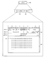
- FIG. 1 is an example of a control method according to the first embodiment.
- FIG. 2 is an example of a control method according to the second embodiment.
- FIG. 3 is an explanatory diagram showing a system configuration example of the system 300.
- FIG. 4 is an explanatory diagram showing an example of the contents stored in the clear flag table 400.
- FIG. 5 is an explanatory diagram (part 1) of a specific example of a packet representing an access request.
- FIG. 6 is an explanatory diagram (part 2) of a specific example of a packet representing an access request.
- FIG. 7 is an explanatory diagram showing an example of a memory cell array of the DRAM 305.
- FIG. 8 is a block diagram illustrating a functional configuration example of the control apparatus 101.
- FIG. 1 is an example of a control method according to the first embodiment.
- FIG. 2 is an example of a control method according to the second embodiment.
- FIG. 3 is an explanatory diagram showing a system configuration example of the system 300.
- FIG. 4
- FIG. 9 is an explanatory diagram illustrating an operation example of the determination unit 802.
- FIG. 10 is an explanatory diagram showing an operation example related to the clear processing of the system 300.
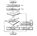
- FIG. 11 is a flowchart (part 1) illustrating an example of the update processing procedure of the control apparatus 101.
- FIG. 12 is a flowchart (part 2) illustrating an example of the update processing procedure of the control apparatus 101.
- FIG. 13 is a flowchart (part 3) illustrating an example of the update processing procedure of the control apparatus 101.
- FIG. 14 is a flowchart illustrating an example of a control processing procedure of the control apparatus 101.
- FIG. 1 is an example of a control method according to the first embodiment.
- a system 100 includes a control device 101, a CPU (Central Processing Unit) 102, and a memory 103.
- a CPU Central Processing Unit
- the control device 101 controls reading / writing of information with respect to the memory 103. Further, the control device 101 controls the refresh operation of the memory 103.
- the CPU 102 governs overall control of the system 100.
- the memory 103 is a storage device that stores information by charging and discharging electric charges. Specifically, for example, the memory 103 stores “1” or “0” information depending on the presence or absence of accumulated charges in the capacitor of the memory cell.
- the memory cell is a circuit that stores 1-bit unit information, and includes a transistor and a capacitor.
- the refresh operation is a memory holding operation in which the same information as the information stored in the memory cell is rewritten to the memory cell.
- the electric charge stored in the memory cell is gradually lost due to a minute leak between the N-type diffusion layer connected to the capacitor and the P-type substrate.
- the memory 103 prevents the stored contents of the memory cell from being lost by periodically performing a refresh operation for rewriting the same information in the memory cell.
- the refresh operation is performed with a period of several ⁇ s or several tens of ⁇ s for each memory cell. That is, an excessive refresh operation in the system 100 leads to an increase in power consumption of the system 100.
- the control apparatus 101 stops the refresh operation for a memory area that does not need to hold information among a plurality of memory areas in the memory 103, thereby reducing the power consumption for the refresh operation of the memory 103. Suppress.
- an operation example of the control device 101 according to the first embodiment will be described.
- the control device 101 detects an access request for a predetermined memory area in the memory 103.
- the access request is a write request or a read request for the memory area.
- the control device 101 detects an access request for the memory area by receiving an access request for the memory area from the CPU 102.
- an access request to the memory area 104 in the memory 103 is detected.
- a write request 110 for the memory area 104 is displayed.
- the control device 101 matches the information stored in the memory area when the charge information is discharged or the read information read from the memory area is read in response to the detected access request. It is determined whether or not.
- the write information is, for example, information to be written included in the data portion 112 of the header portion 111 and the data portion 112 included in the write request 110 for the memory area 104.
- the read information is, for example, information to be read included in the data portion 122 of the header portion 121 and the data portion 122 included in the read response 120 in response to a read request (not shown) to the memory area 104. is there.
- the information stored in each memory cell when the electric charge is discharged is either “1” or “0” information. Whether the information stored in each memory cell is “1” or “0” when the charge is discharged can be arbitrarily set. In the following description, it is assumed that information stored in each memory cell when electric charge is discharged is “0”. In this case, the information stored in the memory area when the charge is discharged is a set of information stored in each memory cell when the charge is discharged, that is, a set of “0”.
- control device 101 when the control device 101 detects a write request 110 for the memory area 104, whether or not all the write information included in the data portion 112 of the write request 110 is “0”. Determine. For example, when the control device 101 detects a read request for the memory area 104, the control device 101 determines whether all the read information included in the data portion 122 of the read response 120 for the read request is “0”.
- the control device 101 controls the refresh operation for the memory area 104 based on the determined determination result. Specifically, for example, when the control apparatus 101 determines that all of the write information or the read information is “0”, the control apparatus 101 stops the refresh operation for the memory area 104. On the other hand, when it is determined that the write information or the read information includes “1”, the control device 101 does not stop the refresh operation for the memory area 104.
- the control device 101 when a write request to the memory area in the memory 103 is detected and the write information written in the memory area is all “0”, the memory area Can be stopped. Further, the control device 101 can detect a read request for the memory area, and can stop the refresh operation for the memory area when all the read information read from the memory area is “0”. As a result, it can be guaranteed that the stored content is “0”, that is, the refresh operation for the memory area that does not need to hold information can be stopped, and the power consumption for the refresh operation of the memory 103 can be suppressed. .
- FIG. 2 is an example of a control method according to the second embodiment. Hereinafter, an example of control processing of the control device 101 according to the second embodiment will be described.
- the control device 101 detects a clear command for a predetermined memory area in the memory 103.
- the clear instruction is an instruction for erasing information stored in the memory area.
- the control device 101 detects a clear command for the memory area by receiving a clear command for the memory area from the CPU 102.
- a clear command 130 for the memory area 104 in the memory 103 is detected. In this case, the information stored in the memory area 104 is cleared.
- control device 101 When the control device 101 detects a clear command for the memory area, it stops the refresh operation for the memory area. That is, if there is a clear command for the memory area, the stored contents of the memory area are cleared, and the control device 101 stops the refresh operation for the memory area. In the example of FIG. 2, when the control device 101 detects a clear command 130 for the memory area 104, the control apparatus 101 stops the refresh operation for the memory area 104.
- the refresh operation for the memory area can be stopped.
- the stored content is “0”, that is, the refresh operation for the memory area that does not need to hold information can be stopped, and the power consumption for the refresh operation of the memory 103 can be suppressed.
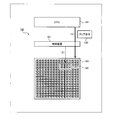
- FIG. 3 is an explanatory diagram showing a system configuration example of the system 300.
- a system 300 includes a CPU 301, an I / F (Interface) 302, an input / output device 303, a ROM (Read-Only Memory) 304, and a DRAM 305. Each component is connected by a bus 310.
- the CPU 301 governs overall control of the system 300.
- the I / F 302 is connected to a network through a communication line, and is connected to another computer via the network. Examples of the network include a LAN (Local Area Network), a WAN (Wide Area Network), and the Internet.
- the I / F 302 controls a network and an internal interface, and controls input / output of data from other computers.
- the input / output device 303 inputs and outputs information.
- Examples of the input / output device 303 include a display device that displays data such as documents, images, and function information, and a keyboard for inputting characters, numbers, and various instructions.
- the ROM 304 is a storage device that stores various programs, for example.
- the DRAM 305 is a storage device used as a main memory, for example.
- the DRAM 305 has a control device 101.
- the control device 101 is a computer that includes an arithmetic device 306 and a storage unit 307 and controls reading / writing of information with respect to the DRAM 305.
- the arithmetic device 306 controls the control device 101.
- the storage unit 307 includes a ROM and a register. Further, the control device 101 controls a refresh operation for the DRAM 305.
- the control device 101 is, for example, a memory controller.
- system 300 may include an external storage device such as a magnetic disk, a magnetic table, and an optical disk in addition to the above-described components.
- an external storage device such as a magnetic disk, a magnetic table, and an optical disk in addition to the above-described components.
- the clear flag table 400 is realized by, for example, the storage unit 307 included in the control device 101 illustrated in FIG.
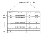
- FIG. 4 is an explanatory diagram showing an example of the contents stored in the clear flag table 400.
- the clear flag table 400 has fields of area ID, address, size, and clear flag. By setting information in each field, clear flag information 400-1 to 400-n is stored as records.
- the area ID is an identifier for identifying the memory area of the DRAM 305.
- the memory area is a storage unit to be controlled by the refresh operation, and is managed in units of pages such as 1 [KB], 4 [KB], and 16 [KB], for example.
- the address is the start address of the memory area.
- the size is the storage capacity of the memory area. The size is specified by a power of 2, for example.
- the unit of size is, for example, [byte].
- the clear flag is a flag indicating whether or not the stored contents of the memory area have been cleared. “Cleared” indicates, for example, a state in which all stored contents of the memory area are “0”. Here, when the clear flag is “Clr”, it indicates that the memory area has been cleared, and when the clear flag is “No-clr”, it indicates that the memory area is not cleared. In the initial state, the memory area clear flag is “No-clr”.
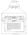
- a packet 500 includes a header part 510 and a data part 520.
- a packet 600 includes a header part 610 and a data part 620.
- each header portion 510, 610 includes identification information (“Requester ID” in the figure) for identifying the request source of the access request.
- each of the header parts 510 and 610 includes an access destination address (“Address” in the figure).
- Each data portion 520, 620 includes write information 521, 621.
- the write information 521 is all “0” information.
- the write information 621 is all “1” information.
- the memory cell array of the DRAM 305 will be described.
- the memory cell array has memory cells arranged in a two-dimensional lattice.
- FIG. 7 is an explanatory diagram showing an example of a memory cell array of the DRAM 305.
- a memory cell array 700 of the DRAM 305 is shown.
- Memory cell array 700 includes a plurality of memory cells arranged in a predetermined row and a predetermined column.
- the DRAM 305 is provided with a read / write circuit for each memory cell.
- Each memory cell is connected to a row address designation signal line and a column address designation signal line, and the read / write circuit detects a signal input to the row and column address designation signal lines to thereby select a memory cell to be controlled. Can be identified.
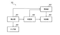
- FIG. 8 is a block diagram illustrating a functional configuration example of the control apparatus 101.
- the control device 101 includes a detection unit 801, a determination unit 802, an update unit 803, a clear unit 804, and a control unit 805.
- Each functional unit may be realized by hardware, for example.
- each functional unit includes AND that is a logical product circuit, INVERTER that is a negative logical circuit, OR that is a logical sum circuit, NOR that is a logical sum negation circuit, and FF (Flip Flop that is a latch circuit). ) Or the like.
- each functional unit may be defined by a function such as Verilog-HDL (Hardware Description Language) and the like, and the description may be logically synthesized and realized by an FPGA (Field Programmable Gate Array).
- Each functional unit may be realized by causing the arithmetic device 306 to execute a program that realizes the function of each functional unit, for example.
- the program is stored in the storage unit 307, for example.
- the detection unit 801 has a function of detecting an access request for a predetermined memory area in the DRAM 305. Specifically, for example, the detection unit 801 detects a write request or a read request for a predetermined memory area by receiving a write request or a read request for the predetermined memory area from the CPU 301.
- access area AR a predetermined memory area serving as an access destination corresponding to an access request
- write request W the write request for the access area AR
- read response R the read response corresponding to the read request for the access area AR
- the detection unit 801 has a function of detecting a clear command for clearing information stored in a predetermined memory area in the DRAM 305. For example, the detection unit 801 detects a clear command for a predetermined memory area by receiving a clear command for the predetermined memory area from the CPU 301.
- a predetermined memory area that is a clear destination corresponding to the clear command may be referred to as a “clear target area CR”.
- a clear command for the clear target area CR may be referred to as “clear command C”.
- the determination unit 802 has a function of determining whether or not all the write information written in the access area AR in response to the detected access request is “0”. Specifically, for example, the determination unit 802 determines whether the write information included in the data portion of the packet representing the detected write request W is all “0”.
- the determination unit 802 determines that all the write information 521 included in the data unit 520 is “0”. In the example of the packet 600 illustrated in FIG. 6, the determination unit 802 determines that “1” is included in the write information 621 included in the data unit 620.
- the determination unit 802 has a function of determining whether or not all read information read from the access area AR in response to the detected access request is “0”. Specifically, for example, the determination unit 802 determines whether or not all the read information included in the data portion of the packet representing the read response R according to the detected read request is “0”. Note that an operation example of the determination unit 802 will be described later with reference to FIG.
- the update unit 803 has a function of updating the clear flag of the memory area Ri. Specifically, for example, when the update unit 803 determines that all pieces of write information written in the access area AR are “0”, the update unit 803 refers to the clear flag table 400 (see FIG. 4), The memory area Ri included in the access area AR is specified from R1 to Rn. Then, the update unit 803 changes the clear flag of the specified memory area Ri to “Clr”.
- the update unit 803 refers to the clear flag table 400 and selects the access area AR from the memory areas R1 to Rn. The memory area Ri included in the is specified. Then, the update unit 803 changes the clear flag of the specified memory area Ri to “Clr”.
- the update unit 803 may change the clear flag of each memory area included in the access area AR to “Clr”.
- the update unit 803 refers to the clear flag table 400 and selects the memory area Ri included in the clear target area CR from the memory areas R1 to Rn. Is identified. Then, the update unit 803 changes the clear flag of the specified memory area Ri to “Clr”.
- the update unit 803 may change the clear flag of each memory area included in the clear target area CR to “Clr”. .
- the clear unit 804 has a function of clearing the stored contents of the clear target area CR when the clear command C for the clear target area CR is detected. Specifically, for example, the clear unit 804 clears the stored contents of the clear target region CR by releasing the charge of each memory cell included in the clear target region CR.
- the clear unit 804 may clear the stored contents of the clear target area CR by overwriting meaningless information on the clear target area CR.
- An example of the operation of the system 300 related to the clear process for clearing the stored contents of the clear target area CR will be described later with reference to FIG.
- the control unit 805 has a function of controlling the refresh operation for the memory area Ri based on the determined determination result. Specifically, for example, when it is determined that all the write information written in the access area AR is “0”, the control unit 805 stops the refresh operation for the access area AR.
- the control unit 805 stops the refresh operation for the access area AR. For example, when the clear command C for the clear target region CR is detected, the control unit 805 stops the refresh operation for the clear target region CR.
- control unit 805 refers to the clear flag table 400 and controls a refresh operation periodically performed on each memory cell of the DRAM 305.
- the control unit 805 refers to the clear flag table 400, and when the clear flag of the memory region Ri selected from the memory regions R1 to Rn is “Clr”, the control unit 805 periodically updates each memory cell in the memory region Ri. The refresh operation performed automatically is stopped.
- the control unit 805 controls, for example, the read / write circuit of the DRAM 305 to refresh each memory cell in the memory area Ri.
- the update unit 803 determines that “1” is included in the write information written to the access area AR, the update unit 803 refers to the clear flag table 400 and selects the access area AR from the memory areas R1 to Rn. A memory area Ri including at least one of the areas is specified. Then, the update unit 803 changes the clear flag of the specified memory area Ri to “No-clr”.
- the update unit 803 sets the clear flag of each memory area including at least one of the access areas AR to “No- change to “clr”.
- control unit 805 restarts the refresh operation for the access area AR.
- the control unit 805 refers to the clear flag table 400, and when the clear flag of the memory region Ri selected from the memory regions R1 to Rn is “No-clr”, the control unit 805 stores the information in the memory region Ri. A refresh operation is performed on each memory cell.
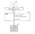
- FIG. 9 is an explanatory diagram illustrating an operation example of the determination unit 802.
- the determination unit 802 stores all the write information included in the data part of the write request W ( ⁇ body> in FIG. 9). It is checked whether it is “0”.
- write information included in the data portion of the write request W is input to the cell 901, and when the write information is all “0”, a signal “true” is output from the cell 901. .
- the “true” signal indicates that the write information is all “0”.
- the determination unit 802 can be realized by applying, for example, an existing ECC (Error Check and Correct) or a parity check mechanism.
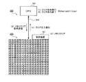
- FIG. 10 is an explanatory diagram showing an operation example related to the clear processing of the system 300.
- the CPU 301 issues a clear command C for the clear target area CR to the control device 101.
- the clear instruction C includes an address “ ⁇ addr>” that specifies the clear target area CR and a size “ ⁇ size>” of the clear target area CR.
- the CPU 301 transmits a memory clear request including the clear command C to the control device 101 via the bus 310.
- the control device 101 clears the stored contents of the clear target area CR specified from the clear command C. Specifically, for example, a plurality of address signal lines for rows and columns are simultaneously specified by the clear command C, and a clear target region CR including a plurality of rows and columns is specified. Then, the clear unit 804 clears the stored contents of the clear target region CR by releasing the charge of each memory cell included in the clear target region CR.
- control device 101 When the clear process for clearing the stored contents of the clear target area CR is completed, the control device 101 generates a clear completion notice and transmits the clear completion notice to the CPU 301 via the bus 310.
- the CPU 301 Upon receiving the clear completion notification, the CPU 301 ends the clear command C. In this way, when the clear process is completed on the control device 101 side, a clear completion notification is sent to the CPU 301 as a bus transaction, the CPU 301 ends the clear command C, and the block of the clear command C is released.
- the clear target area CR can be cleared at a higher speed than in the case where the CPU 301 or the DMA (Direct Memory Access) performs “0” continuous write process.
- DMA Direct Memory Access
- FIG. 11 is a flowchart (part 1) illustrating an example of the update processing procedure of the control apparatus 101.
- the control device 101 extracts the address and size of the access area AR from the access request (step S1101).
- control device 101 scans the data part of the read response R corresponding to the write request W or the read request which is an access request (step S1102). Then, control device 101 determines whether or not all the write information or read information included in the data portion is “0” (step S1103).
- step S1103 when all are “0” (step S1103: Yes), the control apparatus 101 refers to the clear flag table 400, and the memory area Ri included in the access area AR exists in the memory areas R1 to Rn. Whether or not (step S1104).
- the access area AR is specified from the address and size extracted in step S1101.
- step S1104 when the memory area Ri included in the access area AR exists (step S1104: Yes), the control device 101 sets the clear flag of the memory area Ri included in the access area AR in the clear flag table 400 to “Clr”. (Step S1105), and a series of processing according to this flowchart is terminated. On the other hand, when the memory area Ri included in the access area AR does not exist (step S1104: No), the control device 101 ends the series of processes according to this flowchart.
- step S1103 when “1” is included in the write information or the read information (step S1103: No), the control device 101 determines whether the access request is the write request W (step S1106).
- step S1106 when the access request is a read request (step S1106: No), the control device 101 ends a series of processes according to the flowchart.
- the control device 101 refers to the clear flag table 400 and selects at least one of the access areas AR from the memory areas R1 to Rn.
- the memory area Ri to be included is specified (step S1107).
- control device 101 changes the clear flag of the specified memory area Ri in the clear flag table 400 to “No-clr” (step S1108), and ends a series of processes according to this flowchart.
- the memory area Ri included in the access area AR is stored.
- the clear flag can be changed to “Clr”. Further, when “1” is included in the write information written to the access area AR, the clear flag of the memory area Ri including at least one area of the access area AR can be changed to “No-clr”.
- FIG. 12 is a flowchart (part 2) illustrating an example of the update processing procedure of the control apparatus 101.
- the control apparatus 101 extracts the address and size of the access area AR from the write request W for the access area AR (step S1201). ).
- control device 101 scans the data part of the write request W (step S1202). Then, the control device 101 determines whether or not all the write information included in the data part is “0” (step S1203).
- step S1203 when all are “0” (step S1203: Yes), the control apparatus 101 refers to the clear flag table 400, and the memory area Ri included in the access area AR exists in the memory areas R1 to Rn. Whether or not (step S1204).
- step S1204: Yes If the memory area Ri included in the access area AR exists (step S1204: Yes), the control device 101 sets the clear flag of the memory area Ri included in the access area AR in the clear flag table 400 to “Clr”. (Step S1205), and a series of processes according to this flowchart is terminated. On the other hand, when the memory area Ri included in the access area AR does not exist (step S1204: No), the control device 101 ends the series of processes according to this flowchart.
- step S1203 If “1” is included in the write information in step S1203 (step S1203: No), the control device 101 refers to the clear flag table 400 and selects the access area AR from the memory areas R1 to Rn. A memory area Ri including at least one of the areas is specified (step S1206).
- control device 101 changes the clear flag of the specified memory area Ri in the clear flag table 400 to “No-clr” (step S1207), and ends a series of processing according to this flowchart.
- the clear flag of the memory area Ri included in the access area AR can be changed to “Clr”. Further, when “1” is included in the write information written to the access area AR, the clear flag of the memory area Ri including at least one area of the access area AR can be changed to “No-clr”.
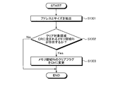
- FIG. 13 is a flowchart (part 3) illustrating an example of the update processing procedure of the control apparatus 101.
- the control device 101 extracts the address and size of the clear target region CR from the clear command C for the clear target region CR (step S1301).
- control device 101 refers to the clear flag table 400 to determine whether or not the memory area Ri included in the clear target area CR exists in the memory areas R1 to Rn (step S1302).
- the clear target area CR is specified from the address and size extracted in step S1301.
- step S1302 when the memory area Ri included in the clear target area CR exists (step S1302: Yes), the control device 101 sets the clear flag of the memory area Ri included in the clear target area CR in the clear flag table 400 to “ It changes to “Clr” (step S1303), and a series of processing according to this flowchart ends.
- step S1302: No when the memory area Ri included in the clear target area CR does not exist (step S1302: No), the control device 101 ends the series of processes according to this flowchart.
- the clear flag of the memory area Ri included in the clear target area CR can be changed to “Clr”.
- the update process of the control device 101 illustrated in FIG. 13 is executed in parallel with, for example, the update process of the control device 101 illustrated in FIG. 11 or the update process of the control device 101 illustrated in FIG.
- This control process is periodically executed, for example, every preset period.
- the period is set such that each memory cell is refreshed at a period of, for example, several ⁇ s or several tens of ⁇ s.
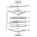
- FIG. 14 is a flowchart illustrating an example of a control processing procedure of the control device 101.
- control device 101 refers to the clear flag table 400 and determines whether or not the clear flag of the memory area Ri is “Clr” (step S1402).
- the control apparatus 101 proceeds to step S1405.
- step S1402 when the clear flag is “No-clr” (step S1402: No), the control device 101 refers to the clear flag table 400 and identifies the address range of the memory area Ri (step S1403). Then, the control device 101 controls the read / write circuit of the DRAM 305 to refresh the memory area Ri in the specified address range (step S1404).
- control device 101 increments “i” in the memory area Ri (step S1405), and determines whether “i” is greater than “n” (step S1406).
- step S1406: No the control apparatus 101 returns to step S1402.
- step S1406 Yes
- the control device 101 ends the series of processes according to this flowchart. Thereby, the refresh operation of the memory region Ri in which the clear flag is “Clr” among the memory regions R1 to Rn can be stopped.
- the control device 101 when the write request W for the access area AR is detected, it is determined whether or not the write information written to the access area AR is all “0”. Can be determined. Then, according to the control device 101, when all the write information written in the access area AR is “0”, the refresh operation for the memory area Ri included in the access area AR can be stopped.
- control device 101 when a read request for the access area AR is detected, it is determined whether or not all pieces of read information read from the access area AR are “0”. be able to. Then, according to the control device 101, when all the read information read from the access area AR is “0”, the refresh operation for the memory area Ri included in the access area AR can be stopped.
- the refresh operation for the memory area Ri included in the clear target area CR can be stopped.
- the control device 101 it is possible to stop the refresh operation for the memory area Ri in which the stored contents are guaranteed to be “0”, and to suppress the power consumption for the refresh operation of the DRAM 305. . Further, by managing the memory area Ri in units of pages such as 1 [KB], 4 [KB], 16 [KB], the refresh operation for the memory area Ri can be efficiently controlled.
- control device 101 when “1” is included in the write information written in the access area AR, at least one area of the access area AR from the memory areas R1 to Rn. Can be specified. Then, the control device 101 can change the clear flag of the specified memory area Ri to “No-clr”.
- control method described in the present embodiment can be realized by executing a prepared program on a computer.
- the control program is recorded on a computer-readable recording medium and executed by being read from the recording medium by the computer.
- the control program may be distributed via a network such as the Internet.
- control apparatus 101 described in the present embodiment includes a special-purpose IC (hereinafter simply referred to as “ASIC”) such as a standard cell or a structured ASIC (Application Specific Integrated Circuit), or a PLD (Programmable Logic) such as an FPGA. It can also be realized by Device). Specifically, for example, the control device 101 can be manufactured by defining the functions of the above-described control device 101 by HDL description, logically synthesizing the HDL description and giving the ASIC or PLD.
- ASIC Application Specific Integrated Circuit
- PLD Programmable Logic
- control device 101 control device 103 memory 305 DRAM 801 detection unit 802 determination unit 803 update unit 804 clear unit 805 control unit
Landscapes
- Engineering & Computer Science (AREA)
- Microelectronics & Electronic Packaging (AREA)
- Computer Hardware Design (AREA)
- Theoretical Computer Science (AREA)
- Physics & Mathematics (AREA)
- General Engineering & Computer Science (AREA)
- General Physics & Mathematics (AREA)
- Dram (AREA)
- Techniques For Improving Reliability Of Storages (AREA)
- Memory System (AREA)
Abstract
Description
図1は、実施の形態1にかかる制御方法の一実施例である。図1において、システム100は、制御装置101と、CPU(Central Processing Unit)102と、メモリ103と、を含む。
つぎに、図2を用いて、実施の形態2にかかる制御方法の一実施例について説明する。実施の形態2では、メモリ103内のメモリ領域に対するクリア命令を用いた制御装置101の動作例について説明する。なお、実施の形態1で説明した箇所と同一箇所については説明を省略する。
つぎに、実施の形態3にかかるシステム300のシステム構成例について説明する。なお、実施の形態1および実施の形態2で説明した箇所と同一箇所については説明を省略する。
つぎに、制御装置101が用いるクリアフラグテーブル400の記憶内容について説明する。クリアフラグテーブル400は、例えば、図3に示した制御装置101が有する記憶部307により実現される。
つぎに、DRAM305内の所定のメモリ領域に対するアクセス要求を表すパケットの具体例について説明する。ここでは、アクセス要求の一例として、メモリ領域に対する書込要求を例に挙げて説明する。
ここで、DRAM305のメモリセルアレイについて説明する。メモリセルアレイは、例えば、メモリセルを2次元の格子状に並べたものである。
つぎに、制御装置101の機能的構成例について説明する。図8は、制御装置101の機能的構成例を示すブロック図である。図8において、制御装置101は、検出部801と、判定部802と、更新部803と、クリア部804と、制御部805と、を含む。各機能部は、例えば、ハードウェアにより実現されてもよい。具体的には、例えば、各機能部は、論理積回路であるAND、否定論理回路であるINVERTER、論理和回路であるOR、論理和否定回路であるNORや、ラッチ回路であるFF(Flip Flop)などの素子によって形成されてもよい。また、各機能部は、例えば、Verilog-HDL(Hardware Description Language)などの記述によって機能定義し、その記述を論理合成してFPGA(Field Programmable Gate Array)によって実現してもよい。また、各機能部は、例えば、各機能部の機能を実現するプログラムを演算装置306に実行させることにより実現されてもよい。当該プログラムは、例えば、記憶部307に記憶されている。
つぎに、上述した判定部802の動作例について説明する。ここでは、アクセス領域ARに対する書込要求Wが検出された場合を例に挙げて、判定部802の動作例について説明する。
つぎに、クリア対象領域CRの記憶内容をクリアするクリア処理にかかるシステム300の動作例について説明する。図10は、システム300のクリア処理にかかる動作例を示す説明図である。
つぎに、クリアフラグテーブル400のメモリ領域Riのクリアフラグを更新する制御装置101の更新処理手順について説明する。ここでは、まず、アクセス領域ARに対するアクセス要求が検出された場合の更新処理手順について説明する。
103 メモリ
305 DRAM
801 検出部
802 判定部
803 更新部
804 クリア部
805 制御部
Claims (8)
- 電荷を充放電することにより情報を記憶するメモリ内の所定のメモリ領域に対するアクセス要求を検出する検出部と、
前記検出部によって検出された前記アクセス要求に応じて前記メモリ領域に書き込まれる書込情報または前記メモリ領域から読み出される読出情報が、電荷が放電された場合に前記メモリ領域に記憶される情報と一致するか否かを判定する判定部と、
前記判定部によって前記書込情報または前記読出情報が、電荷が放電された場合に前記メモリ領域に記憶される情報と一致すると判定された場合、前記メモリ領域に対するリフレッシュ動作を停止させる制御部と、
を有することを特徴とする制御装置。 - 前記検出部は、
前記メモリ領域に記憶されている情報をクリアするクリア命令を検出し、
前記制御部は、
前記検出部によって前記クリア命令が検出された場合、前記メモリ領域に対するリフレッシュ動作を停止させることを特徴とする請求項1に記載の制御装置。 - 前記検出部は、
リフレッシュ動作が停止された前記メモリ領域に対する書込要求を検出し、
前記判定部は、
前記書込要求に応じて前記メモリ領域に書き込まれる書込情報が、電荷が放電された場合に前記メモリ領域に記憶される情報と一致するか否かを判定し、
前記制御部は、
前記書込情報が、電荷が放電された場合に前記メモリ領域に記憶される情報と一致しないと判定された場合、前記メモリ領域に対するリフレッシュ動作を再開させることを特徴とする請求項1または2に記載の制御装置。 - 電荷を充放電することにより情報を記憶するメモリ内の所定のメモリ領域に記憶されている情報をクリアするクリア命令を検出する検出部と、
前記検出部によって前記クリア命令が検出された場合、前記メモリ領域に対するリフレッシュ動作を停止させる制御部と、
を有することを特徴とする制御装置。 - コンピュータが、
電荷を充放電することにより情報を記憶するメモリ内の所定のメモリ領域に対するアクセス要求を検出し、
検出した前記アクセス要求に応じて前記メモリ領域に書き込まれる書込情報または前記メモリ領域から読み出される読出情報が、電荷が放電された場合に前記メモリ領域に記憶される情報と一致するか否かを判定し、
前記書込情報または前記読出情報が、電荷が放電された場合に前記メモリ領域に記憶される情報と一致すると判定した場合、前記メモリ領域に対するリフレッシュ動作を停止させる、
処理を実行することを特徴とする制御方法。 - コンピュータが、
電荷を充放電することにより情報を記憶するメモリ内の所定のメモリ領域に記憶されている情報をクリアするクリア命令を検出し、
前記クリア命令を検出した場合、前記メモリ領域に対するリフレッシュ動作を停止させる、
処理を実行することを特徴とする制御方法。 - コンピュータに、
電荷を充放電することにより情報を記憶するメモリ内の所定のメモリ領域に対するアクセス要求を検出し、
検出した前記アクセス要求に応じて前記メモリ領域に書き込まれる書込情報または前記メモリ領域から読み出される読出情報が、電荷が放電された場合に前記メモリ領域に記憶される情報と一致するか否かを判定し、
前記書込情報または前記読出情報が、電荷が放電された場合に前記メモリ領域に記憶される情報と一致すると判定した場合、前記メモリ領域に対するリフレッシュ動作を停止させる、
処理を実行させることを特徴とする制御プログラム。 - コンピュータに、
電荷を充放電することにより情報を記憶するメモリ内の所定のメモリ領域に記憶されている情報をクリアするクリア命令を検出し、
前記クリア命令を検出した場合、前記メモリ領域に対するリフレッシュ動作を停止させる、
処理を実行させることを特徴とする制御プログラム。
Priority Applications (5)
| Application Number | Priority Date | Filing Date | Title |
|---|---|---|---|
| CN201280073737.5A CN104662609A (zh) | 2012-06-07 | 2012-06-07 | 选择性地进行存储器的更新的控制装置 |
| PCT/JP2012/064723 WO2013183155A1 (ja) | 2012-06-07 | 2012-06-07 | 選択的にメモリのリフレッシュを行う制御装置 |
| JP2014519772A JP5928585B2 (ja) | 2012-06-07 | 2012-06-07 | 選択的にメモリのリフレッシュを行う制御装置 |
| KR1020147033848A KR20150006467A (ko) | 2012-06-07 | 2012-06-07 | 선택적으로 메모리의 리프레시를 행하는 제어 장치 |
| US14/561,847 US20150095604A1 (en) | 2012-06-07 | 2014-12-05 | Control device that selectively refreshes memory |
Applications Claiming Priority (1)
| Application Number | Priority Date | Filing Date | Title |
|---|---|---|---|
| PCT/JP2012/064723 WO2013183155A1 (ja) | 2012-06-07 | 2012-06-07 | 選択的にメモリのリフレッシュを行う制御装置 |
Related Child Applications (1)
| Application Number | Title | Priority Date | Filing Date |
|---|---|---|---|
| US14/561,847 Continuation US20150095604A1 (en) | 2012-06-07 | 2014-12-05 | Control device that selectively refreshes memory |
Publications (1)
| Publication Number | Publication Date |
|---|---|
| WO2013183155A1 true WO2013183155A1 (ja) | 2013-12-12 |
Family
ID=49711571
Family Applications (1)
| Application Number | Title | Priority Date | Filing Date |
|---|---|---|---|
| PCT/JP2012/064723 Ceased WO2013183155A1 (ja) | 2012-06-07 | 2012-06-07 | 選択的にメモリのリフレッシュを行う制御装置 |
Country Status (5)
| Country | Link |
|---|---|
| US (1) | US20150095604A1 (ja) |
| JP (1) | JP5928585B2 (ja) |
| KR (1) | KR20150006467A (ja) |
| CN (1) | CN104662609A (ja) |
| WO (1) | WO2013183155A1 (ja) |
Cited By (3)
| Publication number | Priority date | Publication date | Assignee | Title |
|---|---|---|---|---|
| JP2016524775A (ja) * | 2013-05-14 | 2016-08-18 | クアルコム,インコーポレイテッド | ダイナミックランダムアクセスメモリのスマートリフレッシュのための方法およびシステム |
| JP2017191594A (ja) * | 2016-04-15 | 2017-10-19 | ヴィア アライアンス セミコンダクター カンパニー リミテッド | サニタイズ認識dramコントローラ |
| KR20180137613A (ko) * | 2014-06-09 | 2018-12-27 | 후아웨이 테크놀러지 컴퍼니 리미티드 | 다이나믹 랜덤 액세스 메모리(dram)를 리프레시하기 위한 방법, 장치 및 시스템 |
Families Citing this family (3)
| Publication number | Priority date | Publication date | Assignee | Title |
|---|---|---|---|---|
| KR102395158B1 (ko) * | 2015-05-08 | 2022-05-10 | 에스케이하이닉스 주식회사 | 반도체 메모리 장치 |
| KR102384344B1 (ko) * | 2015-06-03 | 2022-04-07 | 삼성전자주식회사 | 모바일 장치 및 모바일 장치의 동작 방법 |
| JP6712545B2 (ja) * | 2016-12-19 | 2020-06-24 | 日立オートモティブシステムズ株式会社 | 電子制御装置、電子制御システム、及び電子制御方法 |
Citations (3)
| Publication number | Priority date | Publication date | Assignee | Title |
|---|---|---|---|---|
| JPH01146195A (ja) * | 1987-12-02 | 1989-06-08 | Mitsubishi Electric Corp | ダイナミック型半導体記憶装置 |
| JPH0413290A (ja) * | 1990-04-28 | 1992-01-17 | Nec Home Electron Ltd | メモリ制御回路 |
| JP2007527592A (ja) * | 2003-07-01 | 2007-09-27 | インテル コーポレイション | Dramの部分的リフレッシュのための方法及び装置 |
Family Cites Families (28)
| Publication number | Priority date | Publication date | Assignee | Title |
|---|---|---|---|---|
| GB2179219B (en) * | 1985-06-07 | 1989-04-19 | Anamartic Ltd | Electrical data storage elements |
| US5469559A (en) * | 1993-07-06 | 1995-11-21 | Dell Usa, L.P. | Method and apparatus for refreshing a selected portion of a dynamic random access memory |
| JP3714489B2 (ja) * | 1995-03-03 | 2005-11-09 | 株式会社日立製作所 | ダイナミック型ramとメモリモジュール |
| JPH10308090A (ja) * | 1997-05-06 | 1998-11-17 | Ricoh Co Ltd | メモリ装置 |
| US6167484A (en) * | 1998-05-12 | 2000-12-26 | Motorola, Inc. | Method and apparatus for leveraging history bits to optimize memory refresh performance |
| US6542958B1 (en) * | 2000-05-10 | 2003-04-01 | Elan Research | Software control of DRAM refresh to reduce power consumption in a data processing system |
| JP4257056B2 (ja) * | 2001-12-13 | 2009-04-22 | エルピーダメモリ株式会社 | ダイナミック型半導体記憶装置及びリフレッシュ制御方法 |
| US7043599B1 (en) * | 2002-06-20 | 2006-05-09 | Rambus Inc. | Dynamic memory supporting simultaneous refresh and data-access transactions |
| US7010644B2 (en) * | 2002-08-29 | 2006-03-07 | Micron Technology, Inc. | Software refreshed memory device and method |
| US6956782B2 (en) * | 2003-09-30 | 2005-10-18 | Infineon Technologies Ag | Selective bank refresh |
| US7342841B2 (en) * | 2004-12-21 | 2008-03-11 | Intel Corporation | Method, apparatus, and system for active refresh management |
| KR100642759B1 (ko) * | 2005-01-28 | 2006-11-10 | 삼성전자주식회사 | 선택적 리프레쉬가 가능한 반도체 메모리 디바이스 |
| US7711897B1 (en) * | 2005-06-10 | 2010-05-04 | American Megatrends, Inc. | Method, system, apparatus, and computer-readable medium for improving disk array performance |
| JP5082727B2 (ja) * | 2007-09-28 | 2012-11-28 | ソニー株式会社 | 記憶制御装置、記憶制御方法およびコンピュータプログラム |
| US8095725B2 (en) * | 2007-12-31 | 2012-01-10 | Intel Corporation | Device, system, and method of memory allocation |
| US20110202709A1 (en) * | 2008-03-19 | 2011-08-18 | Rambus Inc. | Optimizing storage of common patterns in flash memory |
| JP5286943B2 (ja) * | 2008-05-30 | 2013-09-11 | 富士通株式会社 | メモリクリア機構 |
| US8291194B2 (en) * | 2009-11-16 | 2012-10-16 | Mediatek Inc. | Methods of utilizing address mapping table to manage data access of storage medium without physically accessing storage medium and related storage controllers thereof |
| CN102081964B (zh) * | 2009-11-30 | 2014-12-10 | 国际商业机器公司 | 动态随机访问存储器刷新的方法和系统 |
| US8904092B2 (en) * | 2010-02-10 | 2014-12-02 | Hewlett-Packard Development Company, L.P. | Identifying a location containing invalid data in a storage media |
| US20120203993A1 (en) * | 2011-02-08 | 2012-08-09 | SMART Storage Systems, Inc. | Memory system with tiered queuing and method of operation thereof |
| US20120317376A1 (en) * | 2011-06-10 | 2012-12-13 | Advanced Micro Devices, Inc. | Row buffer register file |
| US9116781B2 (en) * | 2011-10-17 | 2015-08-25 | Rambus Inc. | Memory controller and memory device command protocol |
| US20150340080A1 (en) * | 2012-04-04 | 2015-11-26 | Jean Baptiste Maurice Queru | Refreshing Dynamic Memory |
| KR20140003223A (ko) * | 2012-06-29 | 2014-01-09 | 삼성전자주식회사 | 리프레쉬 파워 매니지먼트를 위한 디램 어드레스 생성 방법 및 리프레쉬 파워 매니지먼트 시스템 |
| US9336855B2 (en) * | 2013-05-14 | 2016-05-10 | Qualcomm Incorporated | Methods and systems for smart refresh of dynamic random access memory |
| CN105493192B (zh) * | 2013-09-01 | 2018-10-19 | 英派尔科技开发有限公司 | Dram中增加的刷新间隔和能量效率 |
| KR102192546B1 (ko) * | 2014-04-22 | 2020-12-18 | 에스케이하이닉스 주식회사 | 반도체 메모리 장치 |
-
2012
- 2012-06-07 WO PCT/JP2012/064723 patent/WO2013183155A1/ja not_active Ceased
- 2012-06-07 JP JP2014519772A patent/JP5928585B2/ja not_active Expired - Fee Related
- 2012-06-07 CN CN201280073737.5A patent/CN104662609A/zh active Pending
- 2012-06-07 KR KR1020147033848A patent/KR20150006467A/ko not_active Ceased
-
2014
- 2014-12-05 US US14/561,847 patent/US20150095604A1/en not_active Abandoned
Patent Citations (3)
| Publication number | Priority date | Publication date | Assignee | Title |
|---|---|---|---|---|
| JPH01146195A (ja) * | 1987-12-02 | 1989-06-08 | Mitsubishi Electric Corp | ダイナミック型半導体記憶装置 |
| JPH0413290A (ja) * | 1990-04-28 | 1992-01-17 | Nec Home Electron Ltd | メモリ制御回路 |
| JP2007527592A (ja) * | 2003-07-01 | 2007-09-27 | インテル コーポレイション | Dramの部分的リフレッシュのための方法及び装置 |
Cited By (4)
| Publication number | Priority date | Publication date | Assignee | Title |
|---|---|---|---|---|
| JP2016524775A (ja) * | 2013-05-14 | 2016-08-18 | クアルコム,インコーポレイテッド | ダイナミックランダムアクセスメモリのスマートリフレッシュのための方法およびシステム |
| KR20180137613A (ko) * | 2014-06-09 | 2018-12-27 | 후아웨이 테크놀러지 컴퍼니 리미티드 | 다이나믹 랜덤 액세스 메모리(dram)를 리프레시하기 위한 방법, 장치 및 시스템 |
| KR102048762B1 (ko) * | 2014-06-09 | 2019-11-26 | 후아웨이 테크놀러지 컴퍼니 리미티드 | 다이나믹 랜덤 액세스 메모리(dram)를 리프레시하기 위한 방법, 장치 및 시스템 |
| JP2017191594A (ja) * | 2016-04-15 | 2017-10-19 | ヴィア アライアンス セミコンダクター カンパニー リミテッド | サニタイズ認識dramコントローラ |
Also Published As
| Publication number | Publication date |
|---|---|
| CN104662609A (zh) | 2015-05-27 |
| JPWO2013183155A1 (ja) | 2016-01-28 |
| KR20150006467A (ko) | 2015-01-16 |
| JP5928585B2 (ja) | 2016-06-01 |
| US20150095604A1 (en) | 2015-04-02 |
Similar Documents
| Publication | Publication Date | Title |
|---|---|---|
| JP5928585B2 (ja) | 選択的にメモリのリフレッシュを行う制御装置 | |
| US10141038B2 (en) | Computer system and memory device | |
| US11194711B2 (en) | Storage device | |
| US20150279441A1 (en) | Most activated memory portion handling | |
| JP6280214B2 (ja) | メモリで制御されるデータ移動及びタイミング | |
| US20150121023A1 (en) | Operating A Memory Management Controller | |
| CN107256717A (zh) | 行锤击刷新命令 | |
| US10153015B2 (en) | Managing disturbance induced errors | |
| KR20120052893A (ko) | 직렬 인터페이스 메모리에서의 병행 판독 및 기입 메모리 동작들 | |
| KR20170121046A (ko) | NVMe 인터페이스를 사용하는 장치에 커널 모드 액세스 및 사용자 모드 액세스를 동시에 제공하는 시스템 및 방법 | |
| EP3005126B1 (en) | Storage systems and aliased memory | |
| KR20100003244A (ko) | 판독 실패 관리 방법 및 시스템 | |
| KR20130136342A (ko) | 반도체 장치 및 그 동작 방법 | |
| CN108345545A (zh) | 在逻辑地址与物理地址之间执行散列式转译的存储装置 | |
| CN103456352A (zh) | 半导体器件及其操作方法 | |
| US9286248B2 (en) | Methods and systems for moving and resizing I/O activity logs | |
| CN104375955A (zh) | 高速缓冲存储器设备及其控制方法 | |
| US20120137107A1 (en) | Method of decaying hot data | |
| US9015388B2 (en) | Controlling access to storage in a computing device | |
| US12182412B2 (en) | Setting durations for which data is stored in a non-volatile memory based on data types | |
| US10705745B2 (en) | Using a memory controller to mange access to a memory based on a memory initialization state indicator | |
| JP5637312B2 (ja) | キャッシュ制御装置及びパイプライン制御方法 | |
| CN107967222A (zh) | 一种SPI-Nand查找数据页的方法及装置 | |
| US20160283386A1 (en) | Sequential access of cache data | |
| CN111352867A (zh) | 存储器元件、存储器系统及存储器元件的读取方法 |
Legal Events
| Date | Code | Title | Description |
|---|---|---|---|
| 121 | Ep: the epo has been informed by wipo that ep was designated in this application |
Ref document number: 12878286 Country of ref document: EP Kind code of ref document: A1 |
|
| ENP | Entry into the national phase |
Ref document number: 2014519772 Country of ref document: JP Kind code of ref document: A |
|
| ENP | Entry into the national phase |
Ref document number: 20147033848 Country of ref document: KR Kind code of ref document: A |
|
| NENP | Non-entry into the national phase |
Ref country code: DE |
|
| 122 | Ep: pct application non-entry in european phase |
Ref document number: 12878286 Country of ref document: EP Kind code of ref document: A1 |