JP2017191943A - セラミックス回路基板の製造方法 - Google Patents
セラミックス回路基板の製造方法 Download PDFInfo
- Publication number
- JP2017191943A JP2017191943A JP2017101086A JP2017101086A JP2017191943A JP 2017191943 A JP2017191943 A JP 2017191943A JP 2017101086 A JP2017101086 A JP 2017101086A JP 2017101086 A JP2017101086 A JP 2017101086A JP 2017191943 A JP2017191943 A JP 2017191943A
- Authority
- JP
- Japan
- Prior art keywords
- circuit board
- brazing material
- ceramic
- copper
- ceramic substrate
- Prior art date
- Legal status (The legal status is an assumption and is not a legal conclusion. Google has not performed a legal analysis and makes no representation as to the accuracy of the status listed.)
- Granted
Links
Images
Classifications
-
- H—ELECTRICITY
- H05—ELECTRIC TECHNIQUES NOT OTHERWISE PROVIDED FOR
- H05K—PRINTED CIRCUITS; CASINGS OR CONSTRUCTIONAL DETAILS OF ELECTRIC APPARATUS; MANUFACTURE OF ASSEMBLAGES OF ELECTRICAL COMPONENTS
- H05K3/00—Apparatus or processes for manufacturing printed circuits
- H05K3/02—Apparatus or processes for manufacturing printed circuits in which the conductive material is applied to the surface of the insulating support and is thereafter removed from such areas of the surface which are not intended for current conducting or shielding
- H05K3/06—Apparatus or processes for manufacturing printed circuits in which the conductive material is applied to the surface of the insulating support and is thereafter removed from such areas of the surface which are not intended for current conducting or shielding the conductive material being removed chemically or electrolytically, e.g. by photo-etch process
- H05K3/061—Etching masks
- H05K3/062—Etching masks consisting of metals or alloys or metallic inorganic compounds
-
- B—PERFORMING OPERATIONS; TRANSPORTING
- B23—MACHINE TOOLS; METAL-WORKING NOT OTHERWISE PROVIDED FOR
- B23K—SOLDERING OR UNSOLDERING; WELDING; CLADDING OR PLATING BY SOLDERING OR WELDING; CUTTING BY APPLYING HEAT LOCALLY, e.g. FLAME CUTTING; WORKING BY LASER BEAM
- B23K1/00—Soldering, e.g. brazing, or unsoldering
- B23K1/0008—Soldering, e.g. brazing, or unsoldering specially adapted for particular articles or work
- B23K1/0016—Soldering of electronic components
-
- C—CHEMISTRY; METALLURGY
- C04—CEMENTS; CONCRETE; ARTIFICIAL STONE; CERAMICS; REFRACTORIES
- C04B—LIME, MAGNESIA; SLAG; CEMENTS; COMPOSITIONS THEREOF, e.g. MORTARS, CONCRETE OR LIKE BUILDING MATERIALS; ARTIFICIAL STONE; CERAMICS; REFRACTORIES; TREATMENT OF NATURAL STONE
- C04B37/00—Joining burned ceramic articles with other burned ceramic articles or other articles by heating
- C04B37/02—Joining burned ceramic articles with other burned ceramic articles or other articles by heating with metallic articles
- C04B37/023—Joining burned ceramic articles with other burned ceramic articles or other articles by heating with metallic articles characterised by the interlayer used
- C04B37/026—Joining burned ceramic articles with other burned ceramic articles or other articles by heating with metallic articles characterised by the interlayer used consisting of metals or metal salts
-
- H—ELECTRICITY
- H05—ELECTRIC TECHNIQUES NOT OTHERWISE PROVIDED FOR
- H05K—PRINTED CIRCUITS; CASINGS OR CONSTRUCTIONAL DETAILS OF ELECTRIC APPARATUS; MANUFACTURE OF ASSEMBLAGES OF ELECTRICAL COMPONENTS
- H05K3/00—Apparatus or processes for manufacturing printed circuits
- H05K3/02—Apparatus or processes for manufacturing printed circuits in which the conductive material is applied to the surface of the insulating support and is thereafter removed from such areas of the surface which are not intended for current conducting or shielding
- H05K3/06—Apparatus or processes for manufacturing printed circuits in which the conductive material is applied to the surface of the insulating support and is thereafter removed from such areas of the surface which are not intended for current conducting or shielding the conductive material being removed chemically or electrolytically, e.g. by photo-etch process
-
- H—ELECTRICITY
- H05—ELECTRIC TECHNIQUES NOT OTHERWISE PROVIDED FOR
- H05K—PRINTED CIRCUITS; CASINGS OR CONSTRUCTIONAL DETAILS OF ELECTRIC APPARATUS; MANUFACTURE OF ASSEMBLAGES OF ELECTRICAL COMPONENTS
- H05K3/00—Apparatus or processes for manufacturing printed circuits
- H05K3/38—Improvement of the adhesion between the insulating substrate and the metal
-
- H—ELECTRICITY
- H10—SEMICONDUCTOR DEVICES; ELECTRIC SOLID-STATE DEVICES NOT OTHERWISE PROVIDED FOR
- H10D—INORGANIC ELECTRIC SEMICONDUCTOR DEVICES
- H10D64/00—Electrodes of devices having potential barriers
- H10D64/01—Manufacture or treatment
- H10D64/011—Manufacture or treatment of electrodes ohmically coupled to a semiconductor
-
- H—ELECTRICITY
- H10—SEMICONDUCTOR DEVICES; ELECTRIC SOLID-STATE DEVICES NOT OTHERWISE PROVIDED FOR
- H10W—GENERIC PACKAGES, INTERCONNECTIONS, CONNECTORS OR OTHER CONSTRUCTIONAL DETAILS OF DEVICES COVERED BY CLASS H10
- H10W40/00—Arrangements for thermal protection or thermal control
- H10W40/20—Arrangements for cooling
- H10W40/25—Arrangements for cooling characterised by their materials
- H10W40/255—Arrangements for cooling characterised by their materials having a laminate or multilayered structure, e.g. direct bond copper [DBC] ceramic substrates
-
- H—ELECTRICITY
- H10—SEMICONDUCTOR DEVICES; ELECTRIC SOLID-STATE DEVICES NOT OTHERWISE PROVIDED FOR
- H10W—GENERIC PACKAGES, INTERCONNECTIONS, CONNECTORS OR OTHER CONSTRUCTIONAL DETAILS OF DEVICES COVERED BY CLASS H10
- H10W70/00—Package substrates; Interposers; Redistribution layers [RDL]
- H10W70/60—Insulating or insulated package substrates; Interposers; Redistribution layers
- H10W70/67—Insulating or insulated package substrates; Interposers; Redistribution layers characterised by their insulating layers or insulating parts
- H10W70/69—Insulating materials thereof
- H10W70/692—Ceramics or glasses
-
- B—PERFORMING OPERATIONS; TRANSPORTING
- B23—MACHINE TOOLS; METAL-WORKING NOT OTHERWISE PROVIDED FOR
- B23K—SOLDERING OR UNSOLDERING; WELDING; CLADDING OR PLATING BY SOLDERING OR WELDING; CUTTING BY APPLYING HEAT LOCALLY, e.g. FLAME CUTTING; WORKING BY LASER BEAM
- B23K2101/00—Articles made by soldering, welding or cutting
- B23K2101/36—Electric or electronic devices
-
- C—CHEMISTRY; METALLURGY
- C04—CEMENTS; CONCRETE; ARTIFICIAL STONE; CERAMICS; REFRACTORIES
- C04B—LIME, MAGNESIA; SLAG; CEMENTS; COMPOSITIONS THEREOF, e.g. MORTARS, CONCRETE OR LIKE BUILDING MATERIALS; ARTIFICIAL STONE; CERAMICS; REFRACTORIES; TREATMENT OF NATURAL STONE
- C04B2235/00—Aspects relating to ceramic starting mixtures or sintered ceramic products
- C04B2235/65—Aspects relating to heat treatments of ceramic bodies such as green ceramics or pre-sintered ceramics, e.g. burning, sintering or melting processes
- C04B2235/658—Atmosphere during thermal treatment
-
- C—CHEMISTRY; METALLURGY
- C04—CEMENTS; CONCRETE; ARTIFICIAL STONE; CERAMICS; REFRACTORIES
- C04B—LIME, MAGNESIA; SLAG; CEMENTS; COMPOSITIONS THEREOF, e.g. MORTARS, CONCRETE OR LIKE BUILDING MATERIALS; ARTIFICIAL STONE; CERAMICS; REFRACTORIES; TREATMENT OF NATURAL STONE
- C04B2235/00—Aspects relating to ceramic starting mixtures or sintered ceramic products
- C04B2235/70—Aspects relating to sintered or melt-casted ceramic products
- C04B2235/96—Properties of ceramic products, e.g. mechanical properties such as strength, toughness, wear resistance
- C04B2235/9607—Thermal properties, e.g. thermal expansion coefficient
-
- C—CHEMISTRY; METALLURGY
- C04—CEMENTS; CONCRETE; ARTIFICIAL STONE; CERAMICS; REFRACTORIES
- C04B—LIME, MAGNESIA; SLAG; CEMENTS; COMPOSITIONS THEREOF, e.g. MORTARS, CONCRETE OR LIKE BUILDING MATERIALS; ARTIFICIAL STONE; CERAMICS; REFRACTORIES; TREATMENT OF NATURAL STONE
- C04B2237/00—Aspects relating to ceramic laminates or to joining of ceramic articles with other articles by heating
- C04B2237/02—Aspects relating to interlayers, e.g. used to join ceramic articles with other articles by heating
- C04B2237/12—Metallic interlayers
- C04B2237/125—Metallic interlayers based on noble metals, e.g. silver
-
- C—CHEMISTRY; METALLURGY
- C04—CEMENTS; CONCRETE; ARTIFICIAL STONE; CERAMICS; REFRACTORIES
- C04B—LIME, MAGNESIA; SLAG; CEMENTS; COMPOSITIONS THEREOF, e.g. MORTARS, CONCRETE OR LIKE BUILDING MATERIALS; ARTIFICIAL STONE; CERAMICS; REFRACTORIES; TREATMENT OF NATURAL STONE
- C04B2237/00—Aspects relating to ceramic laminates or to joining of ceramic articles with other articles by heating
- C04B2237/02—Aspects relating to interlayers, e.g. used to join ceramic articles with other articles by heating
- C04B2237/12—Metallic interlayers
- C04B2237/126—Metallic interlayers wherein the active component for bonding is not the largest fraction of the interlayer
- C04B2237/127—The active component for bonding being a refractory metal
-
- C—CHEMISTRY; METALLURGY
- C04—CEMENTS; CONCRETE; ARTIFICIAL STONE; CERAMICS; REFRACTORIES
- C04B—LIME, MAGNESIA; SLAG; CEMENTS; COMPOSITIONS THEREOF, e.g. MORTARS, CONCRETE OR LIKE BUILDING MATERIALS; ARTIFICIAL STONE; CERAMICS; REFRACTORIES; TREATMENT OF NATURAL STONE
- C04B2237/00—Aspects relating to ceramic laminates or to joining of ceramic articles with other articles by heating
- C04B2237/30—Composition of layers of ceramic laminates or of ceramic or metallic articles to be joined by heating, e.g. Si substrates
- C04B2237/32—Ceramic
- C04B2237/34—Oxidic
- C04B2237/343—Alumina or aluminates
-
- C—CHEMISTRY; METALLURGY
- C04—CEMENTS; CONCRETE; ARTIFICIAL STONE; CERAMICS; REFRACTORIES
- C04B—LIME, MAGNESIA; SLAG; CEMENTS; COMPOSITIONS THEREOF, e.g. MORTARS, CONCRETE OR LIKE BUILDING MATERIALS; ARTIFICIAL STONE; CERAMICS; REFRACTORIES; TREATMENT OF NATURAL STONE
- C04B2237/00—Aspects relating to ceramic laminates or to joining of ceramic articles with other articles by heating
- C04B2237/30—Composition of layers of ceramic laminates or of ceramic or metallic articles to be joined by heating, e.g. Si substrates
- C04B2237/32—Ceramic
- C04B2237/36—Non-oxidic
- C04B2237/366—Aluminium nitride
-
- C—CHEMISTRY; METALLURGY
- C04—CEMENTS; CONCRETE; ARTIFICIAL STONE; CERAMICS; REFRACTORIES
- C04B—LIME, MAGNESIA; SLAG; CEMENTS; COMPOSITIONS THEREOF, e.g. MORTARS, CONCRETE OR LIKE BUILDING MATERIALS; ARTIFICIAL STONE; CERAMICS; REFRACTORIES; TREATMENT OF NATURAL STONE
- C04B2237/00—Aspects relating to ceramic laminates or to joining of ceramic articles with other articles by heating
- C04B2237/30—Composition of layers of ceramic laminates or of ceramic or metallic articles to be joined by heating, e.g. Si substrates
- C04B2237/32—Ceramic
- C04B2237/36—Non-oxidic
- C04B2237/368—Silicon nitride
-
- C—CHEMISTRY; METALLURGY
- C04—CEMENTS; CONCRETE; ARTIFICIAL STONE; CERAMICS; REFRACTORIES
- C04B—LIME, MAGNESIA; SLAG; CEMENTS; COMPOSITIONS THEREOF, e.g. MORTARS, CONCRETE OR LIKE BUILDING MATERIALS; ARTIFICIAL STONE; CERAMICS; REFRACTORIES; TREATMENT OF NATURAL STONE
- C04B2237/00—Aspects relating to ceramic laminates or to joining of ceramic articles with other articles by heating
- C04B2237/50—Processing aspects relating to ceramic laminates or to the joining of ceramic articles with other articles by heating
- C04B2237/70—Forming laminates or joined articles comprising layers of a specific, unusual thickness
- C04B2237/706—Forming laminates or joined articles comprising layers of a specific, unusual thickness of one or more of the metallic layers or articles
-
- C—CHEMISTRY; METALLURGY
- C04—CEMENTS; CONCRETE; ARTIFICIAL STONE; CERAMICS; REFRACTORIES
- C04B—LIME, MAGNESIA; SLAG; CEMENTS; COMPOSITIONS THEREOF, e.g. MORTARS, CONCRETE OR LIKE BUILDING MATERIALS; ARTIFICIAL STONE; CERAMICS; REFRACTORIES; TREATMENT OF NATURAL STONE
- C04B2237/00—Aspects relating to ceramic laminates or to joining of ceramic articles with other articles by heating
- C04B2237/50—Processing aspects relating to ceramic laminates or to the joining of ceramic articles with other articles by heating
- C04B2237/88—Joining of two substrates, where a substantial part of the joining material is present outside of the joint, leading to an outside joining of the joint
-
- H—ELECTRICITY
- H05—ELECTRIC TECHNIQUES NOT OTHERWISE PROVIDED FOR
- H05K—PRINTED CIRCUITS; CASINGS OR CONSTRUCTIONAL DETAILS OF ELECTRIC APPARATUS; MANUFACTURE OF ASSEMBLAGES OF ELECTRICAL COMPONENTS
- H05K1/00—Printed circuits
- H05K1/02—Details
- H05K1/03—Use of materials for the substrate
- H05K1/0306—Inorganic insulating substrates, e.g. ceramic, glass
-
- H—ELECTRICITY
- H05—ELECTRIC TECHNIQUES NOT OTHERWISE PROVIDED FOR
- H05K—PRINTED CIRCUITS; CASINGS OR CONSTRUCTIONAL DETAILS OF ELECTRIC APPARATUS; MANUFACTURE OF ASSEMBLAGES OF ELECTRICAL COMPONENTS
- H05K2201/00—Indexing scheme relating to printed circuits covered by H05K1/00
- H05K2201/03—Conductive materials
- H05K2201/0332—Structure of the conductor
- H05K2201/0335—Layered conductors or foils
- H05K2201/0355—Metal foils
-
- H—ELECTRICITY
- H05—ELECTRIC TECHNIQUES NOT OTHERWISE PROVIDED FOR
- H05K—PRINTED CIRCUITS; CASINGS OR CONSTRUCTIONAL DETAILS OF ELECTRIC APPARATUS; MANUFACTURE OF ASSEMBLAGES OF ELECTRICAL COMPONENTS
- H05K2203/00—Indexing scheme relating to apparatus or processes for manufacturing printed circuits covered by H05K3/00
- H05K2203/01—Tools for processing; Objects used during processing
- H05K2203/0104—Tools for processing; Objects used during processing for patterning or coating
- H05K2203/013—Inkjet printing, e.g. for printing insulating material or resist
-
- H—ELECTRICITY
- H05—ELECTRIC TECHNIQUES NOT OTHERWISE PROVIDED FOR
- H05K—PRINTED CIRCUITS; CASINGS OR CONSTRUCTIONAL DETAILS OF ELECTRIC APPARATUS; MANUFACTURE OF ASSEMBLAGES OF ELECTRICAL COMPONENTS
- H05K2203/00—Indexing scheme relating to apparatus or processes for manufacturing printed circuits covered by H05K3/00
- H05K2203/03—Metal processing
- H05K2203/0392—Pretreatment of metal, e.g. before finish plating, etching
-
- H—ELECTRICITY
- H05—ELECTRIC TECHNIQUES NOT OTHERWISE PROVIDED FOR
- H05K—PRINTED CIRCUITS; CASINGS OR CONSTRUCTIONAL DETAILS OF ELECTRIC APPARATUS; MANUFACTURE OF ASSEMBLAGES OF ELECTRICAL COMPONENTS
- H05K2203/00—Indexing scheme relating to apparatus or processes for manufacturing printed circuits covered by H05K3/00
- H05K2203/04—Soldering or other types of metallurgic bonding
- H05K2203/0465—Shape of solder, e.g. differing from spherical shape, different shapes due to different solder pads
-
- H—ELECTRICITY
- H05—ELECTRIC TECHNIQUES NOT OTHERWISE PROVIDED FOR
- H05K—PRINTED CIRCUITS; CASINGS OR CONSTRUCTIONAL DETAILS OF ELECTRIC APPARATUS; MANUFACTURE OF ASSEMBLAGES OF ELECTRICAL COMPONENTS
- H05K2203/00—Indexing scheme relating to apparatus or processes for manufacturing printed circuits covered by H05K3/00
- H05K2203/05—Patterning and lithography; Masks; Details of resist
- H05K2203/0502—Patterning and lithography
- H05K2203/0545—Pattern for applying drops or paste; Applying a pattern made of drops or paste
-
- H—ELECTRICITY
- H05—ELECTRIC TECHNIQUES NOT OTHERWISE PROVIDED FOR
- H05K—PRINTED CIRCUITS; CASINGS OR CONSTRUCTIONAL DETAILS OF ELECTRIC APPARATUS; MANUFACTURE OF ASSEMBLAGES OF ELECTRICAL COMPONENTS
- H05K2203/00—Indexing scheme relating to apparatus or processes for manufacturing printed circuits covered by H05K3/00
- H05K2203/12—Using specific substances
- H05K2203/125—Inorganic compounds, e.g. silver salt
-
- H—ELECTRICITY
- H05—ELECTRIC TECHNIQUES NOT OTHERWISE PROVIDED FOR
- H05K—PRINTED CIRCUITS; CASINGS OR CONSTRUCTIONAL DETAILS OF ELECTRIC APPARATUS; MANUFACTURE OF ASSEMBLAGES OF ELECTRICAL COMPONENTS
- H05K2203/00—Indexing scheme relating to apparatus or processes for manufacturing printed circuits covered by H05K3/00
- H05K2203/16—Inspection; Monitoring; Aligning
- H05K2203/167—Using mechanical means for positioning, alignment or registration, e.g. using rod-in-hole alignment
-
- H—ELECTRICITY
- H05—ELECTRIC TECHNIQUES NOT OTHERWISE PROVIDED FOR
- H05K—PRINTED CIRCUITS; CASINGS OR CONSTRUCTIONAL DETAILS OF ELECTRIC APPARATUS; MANUFACTURE OF ASSEMBLAGES OF ELECTRICAL COMPONENTS
- H05K3/00—Apparatus or processes for manufacturing printed circuits
- H05K3/02—Apparatus or processes for manufacturing printed circuits in which the conductive material is applied to the surface of the insulating support and is thereafter removed from such areas of the surface which are not intended for current conducting or shielding
- H05K3/06—Apparatus or processes for manufacturing printed circuits in which the conductive material is applied to the surface of the insulating support and is thereafter removed from such areas of the surface which are not intended for current conducting or shielding the conductive material being removed chemically or electrolytically, e.g. by photo-etch process
- H05K3/067—Etchants
-
- H—ELECTRICITY
- H05—ELECTRIC TECHNIQUES NOT OTHERWISE PROVIDED FOR
- H05K—PRINTED CIRCUITS; CASINGS OR CONSTRUCTIONAL DETAILS OF ELECTRIC APPARATUS; MANUFACTURE OF ASSEMBLAGES OF ELECTRICAL COMPONENTS
- H05K3/00—Apparatus or processes for manufacturing printed circuits
- H05K3/10—Apparatus or processes for manufacturing printed circuits in which conductive material is applied to the insulating support in such a manner as to form the desired conductive pattern
- H05K3/20—Apparatus or processes for manufacturing printed circuits in which conductive material is applied to the insulating support in such a manner as to form the desired conductive pattern by affixing prefabricated conductor pattern
- H05K3/202—Apparatus or processes for manufacturing printed circuits in which conductive material is applied to the insulating support in such a manner as to form the desired conductive pattern by affixing prefabricated conductor pattern using self-supporting metal foil pattern
-
- H—ELECTRICITY
- H05—ELECTRIC TECHNIQUES NOT OTHERWISE PROVIDED FOR
- H05K—PRINTED CIRCUITS; CASINGS OR CONSTRUCTIONAL DETAILS OF ELECTRIC APPARATUS; MANUFACTURE OF ASSEMBLAGES OF ELECTRICAL COMPONENTS
- H05K3/00—Apparatus or processes for manufacturing printed circuits
- H05K3/30—Assembling printed circuits with electric components, e.g. with resistors
- H05K3/32—Assembling printed circuits with electric components, e.g. with resistors electrically connecting electric components or wires to printed circuits
- H05K3/34—Assembling printed circuits with electric components, e.g. with resistors electrically connecting electric components or wires to printed circuits by soldering
- H05K3/3465—Application of solder
- H05K3/3485—Application of solder paste, slurry or powder
-
- Y—GENERAL TAGGING OF NEW TECHNOLOGICAL DEVELOPMENTS; GENERAL TAGGING OF CROSS-SECTIONAL TECHNOLOGIES SPANNING OVER SEVERAL SECTIONS OF THE IPC; TECHNICAL SUBJECTS COVERED BY FORMER USPC CROSS-REFERENCE ART COLLECTIONS [XRACs] AND DIGESTS
- Y10—TECHNICAL SUBJECTS COVERED BY FORMER USPC
- Y10T—TECHNICAL SUBJECTS COVERED BY FORMER US CLASSIFICATION
- Y10T29/00—Metal working
- Y10T29/49—Method of mechanical manufacture
- Y10T29/49002—Electrical device making
- Y10T29/49117—Conductor or circuit manufacturing
- Y10T29/49124—On flat or curved insulated base, e.g., printed circuit, etc.
- Y10T29/49155—Manufacturing circuit on or in base
- Y10T29/49156—Manufacturing circuit on or in base with selective destruction of conductive paths
Landscapes
- Engineering & Computer Science (AREA)
- Chemical & Material Sciences (AREA)
- Manufacturing & Machinery (AREA)
- Microelectronics & Electronic Packaging (AREA)
- Ceramic Engineering (AREA)
- Organic Chemistry (AREA)
- Materials Engineering (AREA)
- Structural Engineering (AREA)
- Metallurgy (AREA)
- Mechanical Engineering (AREA)
- Ceramic Products (AREA)
- Manufacturing Of Printed Wiring (AREA)
- Parts Printed On Printed Circuit Boards (AREA)
- Manufacturing Of Printed Circuit Boards (AREA)
- Cooling Or The Like Of Semiconductors Or Solid State Devices (AREA)
- Electric Connection Of Electric Components To Printed Circuits (AREA)
- Structure Of Printed Boards (AREA)
Abstract
Description
第一のマスキングが施されていない領域に、Ag、Cu及びTiを含むろう材層を形成する工程と、
ろう材層上に銅板を載せ、加熱によりセラミックス基板と銅板を接合する工程と、
銅板上の銅回路パターンとなる領域に第二のマスキングを施す工程と、
エッチングにより銅回路パターンを形成する工程と
を備える。
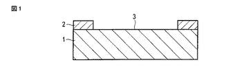
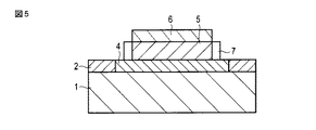
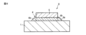
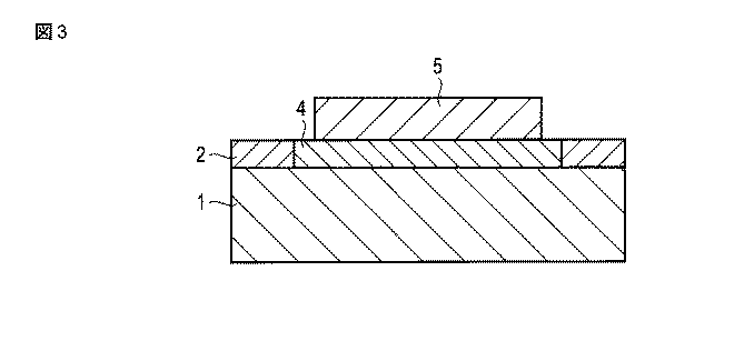
第1の実施形態のセラミックス回路基板は、セラミックス基板と、セラミックス基板の少なくとも一方の面にろう材層を介して接合された銅回路板と、銅回路板の側面から外側にはみ出したろう材層で形成されたろう材はみ出し部とを有する。ろう材層はAg、Cu及びTiを含むろう材から形成される。本発明者らは、ろう材はみ出し部中のTi相およびTiN相の合計を3質量%以上にし、かつその合計量を銅回路板とセラミックス基板の間に介在されたろう材層(以下、接合層と称する)中のTi相およびTiN相の合計量と異なるものにし、さらに、ろう材はみ出し部における1個当たりの面積が200μm2以下の空隙を1つ以下(0を含む)にすることにより、銅回路板と電子部品との熱膨張差による熱ストレスが緩和されると共に接合欠陥が極めて少なくなるため、信頼性の高いセラミックス−金属接合回路基板を実現できることを初めて見出した。
第1の実施形態のセラミックス回路基板は、第2の実施形態の製造方法が一例として示される。
第一のマスキングが施されていない領域に、Ag、Cu及びTiを含むろう材を塗布または印刷することによりろう材層を形成する工程と、
ろう材層上に銅板を載せ、加熱によりセラミックス基板と銅板を接合する工程と、
銅板上の銅回路パターンとなる領域に第二のマスキングを施す工程と、
エッチングにより銅回路パターンを形成する工程と
を有する。
各試料を以下に説明する方法で製造した。まず、50×60mmのセラミックス基板の銅回路パターン形成面に第一のマスキングを行った。第一のマスキングは、銅回路パターンとろう材はみ出し部となる所定のサイズの領域を除いて行った。次に、第一のマスキングを形成していない領域にAg−Cu−Ti系ろう材(Ag67重量%−Cu20重量%−Sn10重量%−Ti3重量%)を厚さ15μmで印刷、また裏面にも厚さ15μmで印刷し、セラミックス基板の両面に銅板を配置し、真空中10−3Pa、800℃で40分間の加熱によりセラミック基板と接合した。銅回路板は、20×20mmの銅板を1mm間隔で2枚配置した。
セラミックス基板(AlN基板)の全面に試料1〜9で用いるのと同様な組成のAg−Cu−Ti系ろう材を厚さ15μmで塗布し、その上に銅板を接合し、加熱接合した。その後、塩化第二鉄で銅板をパターン形状にエッチングし、さらにフッ酸を用いてはみ出しろう材をエッチングした。はみ出し量は試料2と同様に0.12mmとした。はみ出しろう材中の1個当たりの面積200μm2以下の空隙数をカウントしたところ、8個であった。また、試料1〜9と同様の熱サイクル試験を行ったところ、340回となった。
Ag63重量%、Cu32重量%及びTi5重量%を含む活性金属ろう材組成を用いて、銅板と窒化珪素基板(板厚0.32mm)を接合したセラミックス回路基板を製造した。マスキング及び活性金属接合は、試料1〜9で説明したのと同様な条件で行った。
40×60×0.32mmの窒化珪素(Si3N4)基板の銅回路パターン形成面に第一のマスキングを行った。第一のマスキングは、銅回路パターンとろう材はみ出し部となる所定のサイズの領域を除いて行った。次に、第一のマスキングを形成していない領域にAg−Cu−Ti系ろう材を印刷、また裏面にも印刷し、窒化珪素基板の両面に銅板を配置し、真空中10−3Pa、760〜810℃で20〜50分間の加熱により窒化珪素基板と接合した。銅回路板は、15×20×0.3mmの銅板を1mm間隔で2枚配置した。なお、Ag−Cu−Tiろう材の組成およびろう材層厚さは表3の通りとした。なお、窒化珪素(Si3N4)基板は熱伝導率85W/m・Kかつ3点曲げ強度750MPaのものを用いた。
以下に、本願出願の当初の特許請求の範囲に記載された発明を付記する。
[1] セラミックス基板と、
前記セラミックス基板の少なくとも一方の面に、Ag、Cu及びTiを含むろう材層を介して接合された銅回路板と、
前記銅回路板の側面から外側にはみ出した前記ろう材層で形成されたろう材はみ出し部とを備えるセラミックス回路基板であって、
前記ろう材はみ出し部中のTi相およびTiN相の合計は3質量%以上で、かつ前記セラミックス基板と前記銅回路板の間に介在された前記ろう材層中のTi相およびTiN相の合計量と異なり、前記ろう材はみ出し部における1個当たりの面積が200μm 2 以下の空隙が1つ以下(0を含む)であることを特徴とするセラミックス回路基板。
[2] 前記ろう材はみ出し部中のTi相およびTiN相の合計は3質量%以上40質量%以下であることを特徴とする上記[1]記載のセラミックス回路基板。
[3] 前記ろう材はみ出し部のはみ出し長さが0.01mm以上で、かつ前記銅回路板の間隔の30%以下であることを特徴とする上記[1]または[2]のいずれか1項に記載のセラミックス回路基板。
[4] 前記セラミックス基板が窒化珪素、窒化アルミニウムあるいはアルミナからなり、前記銅回路板の厚さが0.25mm以上であることを特徴とする上記[1]ないし上記[3]のいずれか1項に記載のセラミックス回路基板。
[5] 前記ろう材層は、Ag:90〜50重量%、Snおよび/またはInからなる元素:5〜15重量%、Ti:0.1〜6重量%、残部Cuおよび不可避不純物からなる組成のろう材を用いて形成されることを特徴とする請求項1ないし請求項4のいずれか1項に記載のセラミックス回路基板。
[6] セラミックス基板上における、銅回路パターン及びろう材はみ出し部となる領域以外の部分に第一のマスキングを施す工程と、
前記第一のマスキングが施されていない領域に、Ag、Cu及びTiを含むろう材層を形成する工程と、
前記ろう材層上に銅板を載せ、加熱により前記セラミックス基板と前記銅板を接合する工程と、
前記銅板上の銅回路パターンとなる領域に第二のマスキングを施す工程と、
エッチングにより銅回路パターンを形成する工程と
を備えることを特徴とするセラミックス回路基板の製造方法。
[7] 前記エッチングに用いるエッチング液が塩化第二鉄または塩化第二銅であることを特徴とする上記[6]記載のセラミックス回路基板の製造方法。
[8] 前記セラミックス基板と前記銅板に位置合わせ用マーキングが施されていることを特徴とする上記[6]または[7]のいずれか1項に記載のセラミックス基板の製造方法。
[9] 前記第一のマスキング及び前記第二のマスキングの材料が印刷可能な有機インクレジストであることを特徴とする上記[6]ないし上記[8]のいずれか1項に記載のセラミックス回路基板の製造方法。
Claims (9)
- セラミックス基板と、
前記セラミックス基板の少なくとも一方の面に、Ag、Cu及びTiを含むろう材層を介して接合された銅回路板と、
前記銅回路板の側面から外側にはみ出した前記ろう材層で形成されたろう材はみ出し部とを備えるセラミックス回路基板であって、
前記ろう材はみ出し部中のTi相およびTiN相の合計は3質量%以上で、かつ前記セラミックス基板と前記銅回路板の間に介在された前記ろう材層中のTi相およびTiN相の合計量と異なり、前記ろう材はみ出し部における1個当たりの面積が200μm2以下の空隙が1つ以下(0を含む)であることを特徴とするセラミックス回路基板。 - 前記ろう材はみ出し部中のTi相およびTiN相の合計は3質量%以上40質量%以下であることを特徴とする請求項1記載のセラミックス回路基板。
- 前記ろう材はみ出し部のはみ出し長さが0.01mm以上で、かつ前記銅回路板の間隔の30%以下であることを特徴とする請求項1または請求項2のいずれか1項に記載のセラミックス回路基板。
- 前記セラミックス基板が窒化珪素、窒化アルミニウムあるいはアルミナからなり、前記銅回路板の厚さが0.25mm以上であることを特徴とする請求項1ないし請求項3のいずれか1項に記載のセラミックス回路基板。
- 前記ろう材層は、Ag:90〜50重量%、Snおよび/またはInからなる元素:5〜15重量%、Ti:0.1〜6重量%、残部Cuおよび不可避不純物からなる組成のろう材を用いて形成されることを特徴とする請求項1ないし請求項4のいずれか1項に記載のセラミックス回路基板。
- セラミックス基板上における、銅回路パターン及びろう材はみ出し部となる領域以外の部分に第一のマスキングを施す工程と、
前記第一のマスキングが施されていない領域に、Ag、Cu及びTiを含むろう材層を形成する工程と、
前記ろう材層上に銅板を載せ、加熱により前記セラミックス基板と前記銅板を接合する工程と、
前記銅板上の銅回路パターンとなる領域に第二のマスキングを施す工程と、
エッチングにより銅回路パターンを形成する工程と
を備えることを特徴とするセラミックス回路基板の製造方法。 - 前記エッチングに用いるエッチング液が塩化第二鉄または塩化第二銅であることを特徴とする請求項6記載のセラミックス回路基板の製造方法。
- 前記セラミックス基板と前記銅板に位置合わせ用マーキングが施されていることを特徴とする請求項6または請求項7のいずれか1項に記載のセラミックス基板の製造方法。
- 前記第一のマスキング及び前記第二のマスキングの材料が印刷可能な有機インクレジストであることを特徴とする請求項6ないし請求項8のいずれか1項に記載のセラミックス回路基板の製造方法。
Applications Claiming Priority (2)
| Application Number | Priority Date | Filing Date | Title |
|---|---|---|---|
| JP2009213511 | 2009-09-15 | ||
| JP2009213511 | 2009-09-15 |
Related Parent Applications (1)
| Application Number | Title | Priority Date | Filing Date |
|---|---|---|---|
| JP2016075911A Division JP6271629B2 (ja) | 2009-09-15 | 2016-04-05 | パワーモジュール用セラミックス回路基板 |
Publications (2)
| Publication Number | Publication Date |
|---|---|
| JP2017191943A true JP2017191943A (ja) | 2017-10-19 |
| JP6334781B2 JP6334781B2 (ja) | 2018-05-30 |
Family
ID=43758676
Family Applications (7)
| Application Number | Title | Priority Date | Filing Date |
|---|---|---|---|
| JP2011531941A Active JP5637992B2 (ja) | 2009-09-15 | 2010-09-15 | セラミックス回路基板の製造方法 |
| JP2014148865A Active JP6158144B2 (ja) | 2009-09-15 | 2014-07-22 | セラミックス回路基板 |
| JP2016075910A Active JP6271628B2 (ja) | 2009-09-15 | 2016-04-05 | パワーモジュール |
| JP2016075911A Active JP6271629B2 (ja) | 2009-09-15 | 2016-04-05 | パワーモジュール用セラミックス回路基板 |
| JP2017101088A Active JP6400788B2 (ja) | 2009-09-15 | 2017-05-22 | パワーモジュールの製造方法 |
| JP2017101087A Active JP6400787B2 (ja) | 2009-09-15 | 2017-05-22 | パワーモジュール用セラミックス回路基板の製造方法 |
| JP2017101086A Active JP6334781B2 (ja) | 2009-09-15 | 2017-05-22 | セラミックス回路基板の製造方法 |
Family Applications Before (6)
| Application Number | Title | Priority Date | Filing Date |
|---|---|---|---|
| JP2011531941A Active JP5637992B2 (ja) | 2009-09-15 | 2010-09-15 | セラミックス回路基板の製造方法 |
| JP2014148865A Active JP6158144B2 (ja) | 2009-09-15 | 2014-07-22 | セラミックス回路基板 |
| JP2016075910A Active JP6271628B2 (ja) | 2009-09-15 | 2016-04-05 | パワーモジュール |
| JP2016075911A Active JP6271629B2 (ja) | 2009-09-15 | 2016-04-05 | パワーモジュール用セラミックス回路基板 |
| JP2017101088A Active JP6400788B2 (ja) | 2009-09-15 | 2017-05-22 | パワーモジュールの製造方法 |
| JP2017101087A Active JP6400787B2 (ja) | 2009-09-15 | 2017-05-22 | パワーモジュール用セラミックス回路基板の製造方法 |
Country Status (6)
| Country | Link |
|---|---|
| US (2) | US8785785B2 (ja) |
| EP (2) | EP3273755B1 (ja) |
| JP (7) | JP5637992B2 (ja) |
| HU (2) | HUE041380T2 (ja) |
| PL (1) | PL2480052T3 (ja) |
| WO (1) | WO2011034075A1 (ja) |
Cited By (2)
| Publication number | Priority date | Publication date | Assignee | Title |
|---|---|---|---|---|
| JP2022108546A (ja) * | 2021-01-13 | 2022-07-26 | 三菱マテリアル株式会社 | 銅/セラミックス接合体、および、絶縁回路基板 |
| JP2025521949A (ja) * | 2022-07-29 | 2025-07-10 | ヘレウス エレクトロニクス ゲーエムベーハー ウント カンパニー カーゲー | 接触領域を有する金属-セラミック基材 |
Families Citing this family (34)
| Publication number | Priority date | Publication date | Assignee | Title |
|---|---|---|---|---|
| EP3273755B1 (en) * | 2009-09-15 | 2018-11-07 | Kabushiki Kaisha Toshiba | Process for producing a ceramic circuit board |
| CN104011852B (zh) * | 2011-12-20 | 2016-12-21 | 株式会社东芝 | 陶瓷铜电路基板和使用了陶瓷铜电路基板的半导体装置 |
| JP6018297B2 (ja) * | 2013-04-26 | 2016-11-02 | 京セラ株式会社 | 複合積層体および電子装置 |
| JP6430382B2 (ja) | 2013-08-08 | 2018-11-28 | 株式会社東芝 | 回路基板および半導体装置 |
| EP3125286B1 (en) * | 2014-03-26 | 2019-05-08 | Kyocera Corporation | Circuit board and electronic device provided with same |
| US9731384B2 (en) * | 2014-11-18 | 2017-08-15 | Baker Hughes Incorporated | Methods and compositions for brazing |
| DE102015110607A1 (de) * | 2015-07-01 | 2017-01-05 | Epcos Ag | Verfahren zur Herstellung eines elektrischen Bauelements |
| EP3358614B1 (en) * | 2015-09-28 | 2022-12-14 | Kabushiki Kaisha Toshiba | Circuit substrate and semiconductor device |
| CN107251214B (zh) * | 2015-09-28 | 2019-08-27 | 株式会社东芝 | 氮化硅电路基板以及使用了该氮化硅电路基板的半导体模块 |
| EP3398205B1 (en) * | 2015-12-28 | 2019-10-30 | NGK Insulators, Ltd. | Bonded substrate and method for manufacturing bonded substrate |
| KR102129339B1 (ko) * | 2016-06-10 | 2020-07-03 | 다나카 기킨조쿠 고교 가부시키가이샤 | 세라믹스 회로 기판, 및 세라믹스 회로 기판의 제조 방법 |
| EP3486942B1 (en) | 2016-07-14 | 2025-04-02 | Kabushiki Kaisha Toshiba, Inc. | Ceramic circuit board and semiconductor module |
| EP3492441B1 (en) * | 2016-07-28 | 2024-10-16 | Kabushiki Kaisha Toshiba | Joined body, circuit board and semiconductor device |
| WO2018021473A1 (ja) | 2016-07-28 | 2018-02-01 | 株式会社 東芝 | 回路基板および半導体モジュール |
| JP7127641B2 (ja) * | 2017-05-11 | 2022-08-30 | 住友電気工業株式会社 | 半導体装置 |
| WO2019006101A1 (en) * | 2017-06-30 | 2019-01-03 | Kyocera International, Inc. | MICROELECTRONIC BUILDING CONSTRUCTION ACTIVATED BY REINFORCING AND DESIGNING CERAMIC INSULATION |
| CN107369741A (zh) * | 2017-07-13 | 2017-11-21 | 东莞市凯昶德电子科技股份有限公司 | 带一体式金属围坝的led支架模组及其制备方法 |
| WO2019022133A1 (ja) * | 2017-07-25 | 2019-01-31 | デンカ株式会社 | セラミックス回路基板及びその製造方法 |
| US10695875B2 (en) * | 2018-03-19 | 2020-06-30 | Asia Vital Components Co., Ltd. | Soldering method of soldering jig |
| CN112189382A (zh) | 2018-05-23 | 2021-01-05 | 住友电木株式会社 | 电路基板的制造方法 |
| JP7243182B2 (ja) * | 2018-12-26 | 2023-03-22 | 三菱マテリアル株式会社 | 絶縁回路基板の製造方法及びその絶縁回路基板 |
| WO2020184510A1 (ja) * | 2019-03-14 | 2020-09-17 | 日本碍子株式会社 | 接合基板及び接合基板の製造方法 |
| WO2020208698A1 (ja) | 2019-04-09 | 2020-10-15 | 日本碍子株式会社 | 接合基板及び接合基板の製造方法 |
| CN113508462B (zh) | 2019-09-02 | 2024-09-20 | 株式会社东芝 | 接合体、电路基板及半导体装置 |
| CN113053833A (zh) * | 2019-12-26 | 2021-06-29 | 财团法人工业技术研究院 | 一种半导体装置及其制作方法 |
| JP7659223B2 (ja) * | 2020-02-18 | 2025-04-09 | 住友金属鉱山株式会社 | エッチング後フレキシブル基板 |
| JPWO2021200810A1 (ja) * | 2020-03-30 | 2021-10-07 | ||
| DE102020111700B4 (de) | 2020-04-29 | 2024-12-05 | Rogers Germany Gmbh | Trägersubstrat und Verfahren zur Herstellung eines Trägersubstrats |
| JP7672204B2 (ja) * | 2020-07-15 | 2025-05-07 | Dowaメタルテック株式会社 | 絶縁基板およびその製造方法 |
| JP7642678B2 (ja) * | 2020-12-24 | 2025-03-10 | 株式会社東芝 | 絶縁性回路基板およびそれを用いた半導体装置 |
| CN117321020A (zh) * | 2021-05-19 | 2023-12-29 | 株式会社东芝 | 接合体的制造方法及使用了其的陶瓷电路基板的制造方法 |
| WO2023074470A1 (ja) | 2021-10-25 | 2023-05-04 | 株式会社 東芝 | セラミックス銅回路基板およびそれを用いた半導体装置 |
| JP2023066874A (ja) * | 2021-10-29 | 2023-05-16 | 三菱マテリアル株式会社 | 銅/セラミックス接合体、および、絶縁回路基板 |
| JP7576209B2 (ja) * | 2022-11-25 | 2024-10-30 | デンカ株式会社 | 窒化ケイ素焼結体及びその製造方法、接合体、並びに、パワーモジュール |
Citations (4)
| Publication number | Priority date | Publication date | Assignee | Title |
|---|---|---|---|---|
| JPH10326949A (ja) * | 1997-05-26 | 1998-12-08 | Denki Kagaku Kogyo Kk | 回路基板 |
| JP2007173577A (ja) * | 2005-12-22 | 2007-07-05 | Hitachi Metals Ltd | セラミックス回路基板 |
| JP2007281219A (ja) * | 2006-04-07 | 2007-10-25 | Hitachi Metals Ltd | セラミックス回路基板およびその製造方法 |
| WO2008004552A1 (fr) * | 2006-07-04 | 2008-01-10 | Kabushiki Kaisha Toshiba | corps soudé céramique/métal, procédé de fabrication du corps soudé et dispositif semi-conducteur utilisant le corps soudé |
Family Cites Families (23)
| Publication number | Priority date | Publication date | Assignee | Title |
|---|---|---|---|---|
| FR1393352A (fr) * | 1963-01-21 | 1965-03-26 | Ibm | Fabricaition de micro-circuits |
| US5541368A (en) * | 1994-07-15 | 1996-07-30 | Dell Usa, L.P. | Laminated multi chip module interconnect apparatus |
| JPH10190176A (ja) | 1996-12-26 | 1998-07-21 | Denki Kagaku Kogyo Kk | 回路基板 |
| US6286206B1 (en) * | 1997-02-25 | 2001-09-11 | Chou H. Li | Heat-resistant electronic systems and circuit boards |
| TW453137B (en) * | 1997-08-25 | 2001-09-01 | Showa Denko Kk | Electrode structure of silicon semiconductor device and the manufacturing method of silicon device using it |
| JP3447532B2 (ja) * | 1997-09-19 | 2003-09-16 | 科学技術振興事業団 | ろう付け用構造体およびメタライズ構造体 |
| JP3847954B2 (ja) | 1998-05-22 | 2006-11-22 | 株式会社東芝 | セラミックス回路基板の製造方法 |
| US6700053B2 (en) * | 2000-07-03 | 2004-03-02 | Komatsu Ltd. | Thermoelectric module |
| DE10165080B4 (de) * | 2000-09-20 | 2015-05-13 | Hitachi Metals, Ltd. | Siliciumnitrid-Pulver und -Sinterkörper sowie Verfahren zu deren Herstellung und Leiterplatte damit |
| JP5038565B2 (ja) * | 2000-09-22 | 2012-10-03 | 株式会社東芝 | セラミックス回路基板およびその製造方法 |
| WO2002061765A1 (en) * | 2001-01-29 | 2002-08-08 | Jsr Corporation | Composite particle for dielectrics, ultramicroparticulate composite resin particle, composition for forming dielectrics and use thereof |
| JP4887583B2 (ja) * | 2001-08-09 | 2012-02-29 | Dowaメタルテック株式会社 | セラミックス回路基板の製造方法 |
| JP3648189B2 (ja) * | 2001-09-28 | 2005-05-18 | 同和鉱業株式会社 | 金属−セラミックス回路基板 |
| JP4362597B2 (ja) * | 2003-05-30 | 2009-11-11 | Dowaメタルテック株式会社 | 金属−セラミックス回路基板およびその製造方法 |
| JP3816508B2 (ja) * | 2004-11-04 | 2006-08-30 | 三井金属鉱業株式会社 | キャパシタ層形成材及びそのキャパシタ層形成材を用いて得られる内蔵キャパシタ層を備えたプリント配線板 |
| JP4345066B2 (ja) * | 2005-05-24 | 2009-10-14 | 日立金属株式会社 | セラミックス回路基板及びこれを用いたパワー半導体モジュール |
| JP5186719B2 (ja) * | 2005-08-29 | 2013-04-24 | 日立金属株式会社 | セラミックス配線基板、その製造方法及び半導体モジュール |
| JP5258045B2 (ja) * | 2006-06-30 | 2013-08-07 | 日本電気株式会社 | 配線基板、配線基板を用いた半導体装置、及びそれらの製造方法 |
| JP2009170930A (ja) * | 2009-03-12 | 2009-07-30 | Hitachi Metals Ltd | セラミックス回路基板及びこれを用いたパワー半導体モジュール |
| EP3273755B1 (en) * | 2009-09-15 | 2018-11-07 | Kabushiki Kaisha Toshiba | Process for producing a ceramic circuit board |
| CN102549738B (zh) * | 2010-05-18 | 2015-07-01 | 丰田自动车株式会社 | 半导体装置及其制造方法 |
| JP5725178B2 (ja) * | 2011-06-30 | 2015-05-27 | 日立金属株式会社 | ろう材、ろう材ペースト、セラミックス回路基板、セラミックスマスター回路基板及びパワー半導体モジュール |
| JP6128367B2 (ja) * | 2012-08-28 | 2017-05-17 | 東芝ライテック株式会社 | 発光装置、および配線基板の製造方法 |
-
2010
- 2010-09-15 EP EP17185117.3A patent/EP3273755B1/en active Active
- 2010-09-15 EP EP10817188.5A patent/EP2480052B1/en active Active
- 2010-09-15 HU HUE17185117A patent/HUE041380T2/hu unknown
- 2010-09-15 JP JP2011531941A patent/JP5637992B2/ja active Active
- 2010-09-15 WO PCT/JP2010/065914 patent/WO2011034075A1/ja not_active Ceased
- 2010-09-15 HU HUE10817188A patent/HUE034429T2/en unknown
- 2010-09-15 PL PL10817188T patent/PL2480052T3/pl unknown
-
2012
- 2012-03-13 US US13/418,813 patent/US8785785B2/en active Active
-
2014
- 2014-06-17 US US14/306,887 patent/US9101065B2/en active Active
- 2014-07-22 JP JP2014148865A patent/JP6158144B2/ja active Active
-
2016
- 2016-04-05 JP JP2016075910A patent/JP6271628B2/ja active Active
- 2016-04-05 JP JP2016075911A patent/JP6271629B2/ja active Active
-
2017
- 2017-05-22 JP JP2017101088A patent/JP6400788B2/ja active Active
- 2017-05-22 JP JP2017101087A patent/JP6400787B2/ja active Active
- 2017-05-22 JP JP2017101086A patent/JP6334781B2/ja active Active
Patent Citations (4)
| Publication number | Priority date | Publication date | Assignee | Title |
|---|---|---|---|---|
| JPH10326949A (ja) * | 1997-05-26 | 1998-12-08 | Denki Kagaku Kogyo Kk | 回路基板 |
| JP2007173577A (ja) * | 2005-12-22 | 2007-07-05 | Hitachi Metals Ltd | セラミックス回路基板 |
| JP2007281219A (ja) * | 2006-04-07 | 2007-10-25 | Hitachi Metals Ltd | セラミックス回路基板およびその製造方法 |
| WO2008004552A1 (fr) * | 2006-07-04 | 2008-01-10 | Kabushiki Kaisha Toshiba | corps soudé céramique/métal, procédé de fabrication du corps soudé et dispositif semi-conducteur utilisant le corps soudé |
Cited By (3)
| Publication number | Priority date | Publication date | Assignee | Title |
|---|---|---|---|---|
| JP2022108546A (ja) * | 2021-01-13 | 2022-07-26 | 三菱マテリアル株式会社 | 銅/セラミックス接合体、および、絶縁回路基板 |
| JP7540345B2 (ja) | 2021-01-13 | 2024-08-27 | 三菱マテリアル株式会社 | 銅/セラミックス接合体、および、絶縁回路基板 |
| JP2025521949A (ja) * | 2022-07-29 | 2025-07-10 | ヘレウス エレクトロニクス ゲーエムベーハー ウント カンパニー カーゲー | 接触領域を有する金属-セラミック基材 |
Also Published As
| Publication number | Publication date |
|---|---|
| JP6400787B2 (ja) | 2018-10-03 |
| US20120168209A1 (en) | 2012-07-05 |
| JP2017195378A (ja) | 2017-10-26 |
| EP3273755A1 (en) | 2018-01-24 |
| JP2017147470A (ja) | 2017-08-24 |
| PL2480052T3 (pl) | 2018-01-31 |
| US9101065B2 (en) | 2015-08-04 |
| EP2480052A1 (en) | 2012-07-25 |
| JP2016165000A (ja) | 2016-09-08 |
| JP5637992B2 (ja) | 2014-12-10 |
| JP6400788B2 (ja) | 2018-10-03 |
| JP6271629B2 (ja) | 2018-01-31 |
| JP6158144B2 (ja) | 2017-07-05 |
| EP2480052B1 (en) | 2017-08-09 |
| WO2011034075A1 (ja) | 2011-03-24 |
| JP2014207482A (ja) | 2014-10-30 |
| US20140291385A1 (en) | 2014-10-02 |
| HUE034429T2 (en) | 2018-02-28 |
| JP6271628B2 (ja) | 2018-01-31 |
| HUE041380T2 (hu) | 2019-05-28 |
| US8785785B2 (en) | 2014-07-22 |
| JP6334781B2 (ja) | 2018-05-30 |
| EP2480052A4 (en) | 2016-01-27 |
| JPWO2011034075A1 (ja) | 2013-02-14 |
| JP2016165001A (ja) | 2016-09-08 |
| EP3273755B1 (en) | 2018-11-07 |
Similar Documents
| Publication | Publication Date | Title |
|---|---|---|
| JP6400787B2 (ja) | パワーモジュール用セラミックス回路基板の製造方法 | |
| US8563869B2 (en) | Circuit board and semiconductor module using this, production method for circuit board | |
| JP2009147316A (ja) | パワーモジュール用基板の製造方法、パワーモジュール用基板、及びパワーモジュール | |
| JP2022161988A (ja) | セラミックス回路基板及びその製造方法 | |
| KR102118271B1 (ko) | 세라믹스/알루미늄 접합체, 절연 회로 기판, 파워 모듈, led 모듈, 열전 모듈 | |
| CN101529588A (zh) | 功率模块用基板以及功率模块用基板的制造方法、及功率模块 | |
| CN106537580B (zh) | 陶瓷电路基板及其制造方法 | |
| JP2013211546A (ja) | セラミックス−銅接合体およびその製造方法 | |
| KR20160124118A (ko) | 세라믹스 회로 기판 | |
| WO2018225809A1 (ja) | セラミックス回路基板 | |
| JP2014118310A (ja) | セラミックス回路基板 | |
| JP6656657B2 (ja) | セラミックス/アルミニウム接合体、パワーモジュール用基板、及び、パワーモジュール | |
| KR20070079929A (ko) | 적층체의 검사 방법 및 히트 스프레더 모듈의 검사 방법 | |
| JP5812882B2 (ja) | 配線基板および電子装置 | |
| JP6307386B2 (ja) | セラミックス回路基板 | |
| JP6088129B2 (ja) | 多層セラミック基板の製造方法 | |
| JP2014029964A (ja) | 接合体の製造方法、パワーモジュールの製造方法、及びパワーモジュール | |
| JP4408889B2 (ja) | セラミックス−金属複合回路基板の製造方法 | |
| JP2020132477A (ja) | 金属−セラミックス接合基板およびその製造方法 | |
| JP2005311382A (ja) | セラミックス−金属複合回路基板及びその製造方法 |
Legal Events
| Date | Code | Title | Description |
|---|---|---|---|
| A977 | Report on retrieval |
Free format text: JAPANESE INTERMEDIATE CODE: A971007 Effective date: 20180326 |
|
| TRDD | Decision of grant or rejection written | ||
| A01 | Written decision to grant a patent or to grant a registration (utility model) |
Free format text: JAPANESE INTERMEDIATE CODE: A01 Effective date: 20180403 |
|
| A61 | First payment of annual fees (during grant procedure) |
Free format text: JAPANESE INTERMEDIATE CODE: A61 Effective date: 20180426 |
|
| R150 | Certificate of patent or registration of utility model |
Ref document number: 6334781 Country of ref document: JP Free format text: JAPANESE INTERMEDIATE CODE: R150 |
|
| S111 | Request for change of ownership or part of ownership |
Free format text: JAPANESE INTERMEDIATE CODE: R313117 |
|
| S533 | Written request for registration of change of name |
Free format text: JAPANESE INTERMEDIATE CODE: R313533 |
|
| R350 | Written notification of registration of transfer |
Free format text: JAPANESE INTERMEDIATE CODE: R350 |
|
| R350 | Written notification of registration of transfer |
Free format text: JAPANESE INTERMEDIATE CODE: R350 |