JP2017201665A - 表示装置 - Google Patents
表示装置 Download PDFInfo
- Publication number
- JP2017201665A JP2017201665A JP2016093071A JP2016093071A JP2017201665A JP 2017201665 A JP2017201665 A JP 2017201665A JP 2016093071 A JP2016093071 A JP 2016093071A JP 2016093071 A JP2016093071 A JP 2016093071A JP 2017201665 A JP2017201665 A JP 2017201665A
- Authority
- JP
- Japan
- Prior art keywords
- tft
- display device
- ltps
- taos
- mos
- Prior art date
- Legal status (The legal status is an assumption and is not a legal conclusion. Google has not performed a legal analysis and makes no representation as to the accuracy of the status listed.)
- Granted
Links
Images








Classifications
-
- H—ELECTRICITY
- H10—SEMICONDUCTOR DEVICES; ELECTRIC SOLID-STATE DEVICES NOT OTHERWISE PROVIDED FOR
- H10D—INORGANIC ELECTRIC SEMICONDUCTOR DEVICES
- H10D86/00—Integrated devices formed in or on insulating or conducting substrates, e.g. formed in silicon-on-insulator [SOI] substrates or on stainless steel or glass substrates
- H10D86/01—Manufacture or treatment
- H10D86/021—Manufacture or treatment of multiple TFTs
- H10D86/0231—Manufacture or treatment of multiple TFTs using masks, e.g. half-tone masks
-
- H—ELECTRICITY
- H10—SEMICONDUCTOR DEVICES; ELECTRIC SOLID-STATE DEVICES NOT OTHERWISE PROVIDED FOR
- H10D—INORGANIC ELECTRIC SEMICONDUCTOR DEVICES
- H10D30/00—Field-effect transistors [FET]
- H10D30/60—Insulated-gate field-effect transistors [IGFET]
- H10D30/67—Thin-film transistors [TFT]
- H10D30/674—Thin-film transistors [TFT] characterised by the active materials
- H10D30/6755—Oxide semiconductors, e.g. zinc oxide, copper aluminium oxide or cadmium stannate
- H10D30/6756—Amorphous oxide semiconductors
-
- G—PHYSICS
- G02—OPTICS
- G02F—OPTICAL DEVICES OR ARRANGEMENTS FOR THE CONTROL OF LIGHT BY MODIFICATION OF THE OPTICAL PROPERTIES OF THE MEDIA OF THE ELEMENTS INVOLVED THEREIN; NON-LINEAR OPTICS; FREQUENCY-CHANGING OF LIGHT; OPTICAL LOGIC ELEMENTS; OPTICAL ANALOGUE/DIGITAL CONVERTERS
- G02F1/00—Devices or arrangements for the control of the intensity, colour, phase, polarisation or direction of light arriving from an independent light source, e.g. switching, gating or modulating; Non-linear optics
- G02F1/01—Devices or arrangements for the control of the intensity, colour, phase, polarisation or direction of light arriving from an independent light source, e.g. switching, gating or modulating; Non-linear optics for the control of the intensity, phase, polarisation or colour
- G02F1/13—Devices or arrangements for the control of the intensity, colour, phase, polarisation or direction of light arriving from an independent light source, e.g. switching, gating or modulating; Non-linear optics for the control of the intensity, phase, polarisation or colour based on liquid crystals, e.g. single liquid crystal display cells
- G02F1/133—Constructional arrangements; Operation of liquid crystal cells; Circuit arrangements
- G02F1/136—Liquid crystal cells structurally associated with a semi-conducting layer or substrate, e.g. cells forming part of an integrated circuit
- G02F1/1362—Active matrix addressed cells
- G02F1/136227—Through-hole connection of the pixel electrode to the active element through an insulation layer
-
- G—PHYSICS
- G02—OPTICS
- G02F—OPTICAL DEVICES OR ARRANGEMENTS FOR THE CONTROL OF LIGHT BY MODIFICATION OF THE OPTICAL PROPERTIES OF THE MEDIA OF THE ELEMENTS INVOLVED THEREIN; NON-LINEAR OPTICS; FREQUENCY-CHANGING OF LIGHT; OPTICAL LOGIC ELEMENTS; OPTICAL ANALOGUE/DIGITAL CONVERTERS
- G02F1/00—Devices or arrangements for the control of the intensity, colour, phase, polarisation or direction of light arriving from an independent light source, e.g. switching, gating or modulating; Non-linear optics
- G02F1/01—Devices or arrangements for the control of the intensity, colour, phase, polarisation or direction of light arriving from an independent light source, e.g. switching, gating or modulating; Non-linear optics for the control of the intensity, phase, polarisation or colour
- G02F1/13—Devices or arrangements for the control of the intensity, colour, phase, polarisation or direction of light arriving from an independent light source, e.g. switching, gating or modulating; Non-linear optics for the control of the intensity, phase, polarisation or colour based on liquid crystals, e.g. single liquid crystal display cells
- G02F1/133—Constructional arrangements; Operation of liquid crystal cells; Circuit arrangements
- G02F1/136—Liquid crystal cells structurally associated with a semi-conducting layer or substrate, e.g. cells forming part of an integrated circuit
- G02F1/1362—Active matrix addressed cells
- G02F1/1368—Active matrix addressed cells in which the switching element is a three-electrode device
-
- H—ELECTRICITY
- H10—SEMICONDUCTOR DEVICES; ELECTRIC SOLID-STATE DEVICES NOT OTHERWISE PROVIDED FOR
- H10D—INORGANIC ELECTRIC SEMICONDUCTOR DEVICES
- H10D86/00—Integrated devices formed in or on insulating or conducting substrates, e.g. formed in silicon-on-insulator [SOI] substrates or on stainless steel or glass substrates
- H10D86/01—Manufacture or treatment
- H10D86/021—Manufacture or treatment of multiple TFTs
- H10D86/0221—Manufacture or treatment of multiple TFTs comprising manufacture, treatment or patterning of TFT semiconductor bodies
-
- H—ELECTRICITY
- H10—SEMICONDUCTOR DEVICES; ELECTRIC SOLID-STATE DEVICES NOT OTHERWISE PROVIDED FOR
- H10D—INORGANIC ELECTRIC SEMICONDUCTOR DEVICES
- H10D86/00—Integrated devices formed in or on insulating or conducting substrates, e.g. formed in silicon-on-insulator [SOI] substrates or on stainless steel or glass substrates
- H10D86/40—Integrated devices formed in or on insulating or conducting substrates, e.g. formed in silicon-on-insulator [SOI] substrates or on stainless steel or glass substrates characterised by multiple TFTs
- H10D86/421—Integrated devices formed in or on insulating or conducting substrates, e.g. formed in silicon-on-insulator [SOI] substrates or on stainless steel or glass substrates characterised by multiple TFTs having a particular composition, shape or crystalline structure of the active layer
-
- H—ELECTRICITY
- H10—SEMICONDUCTOR DEVICES; ELECTRIC SOLID-STATE DEVICES NOT OTHERWISE PROVIDED FOR
- H10D—INORGANIC ELECTRIC SEMICONDUCTOR DEVICES
- H10D86/00—Integrated devices formed in or on insulating or conducting substrates, e.g. formed in silicon-on-insulator [SOI] substrates or on stainless steel or glass substrates
- H10D86/40—Integrated devices formed in or on insulating or conducting substrates, e.g. formed in silicon-on-insulator [SOI] substrates or on stainless steel or glass substrates characterised by multiple TFTs
- H10D86/421—Integrated devices formed in or on insulating or conducting substrates, e.g. formed in silicon-on-insulator [SOI] substrates or on stainless steel or glass substrates characterised by multiple TFTs having a particular composition, shape or crystalline structure of the active layer
- H10D86/423—Integrated devices formed in or on insulating or conducting substrates, e.g. formed in silicon-on-insulator [SOI] substrates or on stainless steel or glass substrates characterised by multiple TFTs having a particular composition, shape or crystalline structure of the active layer comprising semiconductor materials not belonging to the Group IV, e.g. InGaZnO
-
- H—ELECTRICITY
- H10—SEMICONDUCTOR DEVICES; ELECTRIC SOLID-STATE DEVICES NOT OTHERWISE PROVIDED FOR
- H10D—INORGANIC ELECTRIC SEMICONDUCTOR DEVICES
- H10D86/00—Integrated devices formed in or on insulating or conducting substrates, e.g. formed in silicon-on-insulator [SOI] substrates or on stainless steel or glass substrates
- H10D86/40—Integrated devices formed in or on insulating or conducting substrates, e.g. formed in silicon-on-insulator [SOI] substrates or on stainless steel or glass substrates characterised by multiple TFTs
- H10D86/421—Integrated devices formed in or on insulating or conducting substrates, e.g. formed in silicon-on-insulator [SOI] substrates or on stainless steel or glass substrates characterised by multiple TFTs having a particular composition, shape or crystalline structure of the active layer
- H10D86/425—Integrated devices formed in or on insulating or conducting substrates, e.g. formed in silicon-on-insulator [SOI] substrates or on stainless steel or glass substrates characterised by multiple TFTs having a particular composition, shape or crystalline structure of the active layer having different crystal properties in different TFTs or within an individual TFT
-
- H—ELECTRICITY
- H10—SEMICONDUCTOR DEVICES; ELECTRIC SOLID-STATE DEVICES NOT OTHERWISE PROVIDED FOR
- H10D—INORGANIC ELECTRIC SEMICONDUCTOR DEVICES
- H10D86/00—Integrated devices formed in or on insulating or conducting substrates, e.g. formed in silicon-on-insulator [SOI] substrates or on stainless steel or glass substrates
- H10D86/40—Integrated devices formed in or on insulating or conducting substrates, e.g. formed in silicon-on-insulator [SOI] substrates or on stainless steel or glass substrates characterised by multiple TFTs
- H10D86/421—Integrated devices formed in or on insulating or conducting substrates, e.g. formed in silicon-on-insulator [SOI] substrates or on stainless steel or glass substrates characterised by multiple TFTs having a particular composition, shape or crystalline structure of the active layer
- H10D86/427—Integrated devices formed in or on insulating or conducting substrates, e.g. formed in silicon-on-insulator [SOI] substrates or on stainless steel or glass substrates characterised by multiple TFTs having a particular composition, shape or crystalline structure of the active layer having different thicknesses of the semiconductor bodies in different TFTs
-
- H—ELECTRICITY
- H10—SEMICONDUCTOR DEVICES; ELECTRIC SOLID-STATE DEVICES NOT OTHERWISE PROVIDED FOR
- H10D—INORGANIC ELECTRIC SEMICONDUCTOR DEVICES
- H10D86/00—Integrated devices formed in or on insulating or conducting substrates, e.g. formed in silicon-on-insulator [SOI] substrates or on stainless steel or glass substrates
- H10D86/40—Integrated devices formed in or on insulating or conducting substrates, e.g. formed in silicon-on-insulator [SOI] substrates or on stainless steel or glass substrates characterised by multiple TFTs
- H10D86/441—Interconnections, e.g. scanning lines
-
- H—ELECTRICITY
- H10—SEMICONDUCTOR DEVICES; ELECTRIC SOLID-STATE DEVICES NOT OTHERWISE PROVIDED FOR
- H10D—INORGANIC ELECTRIC SEMICONDUCTOR DEVICES
- H10D86/00—Integrated devices formed in or on insulating or conducting substrates, e.g. formed in silicon-on-insulator [SOI] substrates or on stainless steel or glass substrates
- H10D86/40—Integrated devices formed in or on insulating or conducting substrates, e.g. formed in silicon-on-insulator [SOI] substrates or on stainless steel or glass substrates characterised by multiple TFTs
- H10D86/471—Integrated devices formed in or on insulating or conducting substrates, e.g. formed in silicon-on-insulator [SOI] substrates or on stainless steel or glass substrates characterised by multiple TFTs having different architectures, e.g. having both top-gate and bottom-gate TFTs
-
- H—ELECTRICITY
- H10—SEMICONDUCTOR DEVICES; ELECTRIC SOLID-STATE DEVICES NOT OTHERWISE PROVIDED FOR
- H10D—INORGANIC ELECTRIC SEMICONDUCTOR DEVICES
- H10D86/00—Integrated devices formed in or on insulating or conducting substrates, e.g. formed in silicon-on-insulator [SOI] substrates or on stainless steel or glass substrates
- H10D86/40—Integrated devices formed in or on insulating or conducting substrates, e.g. formed in silicon-on-insulator [SOI] substrates or on stainless steel or glass substrates characterised by multiple TFTs
- H10D86/60—Integrated devices formed in or on insulating or conducting substrates, e.g. formed in silicon-on-insulator [SOI] substrates or on stainless steel or glass substrates characterised by multiple TFTs wherein the TFTs are in active matrices
-
- H—ELECTRICITY
- H10—SEMICONDUCTOR DEVICES; ELECTRIC SOLID-STATE DEVICES NOT OTHERWISE PROVIDED FOR
- H10K—ORGANIC ELECTRIC SOLID-STATE DEVICES
- H10K59/00—Integrated devices, or assemblies of multiple devices, comprising at least one organic light-emitting element covered by group H10K50/00
- H10K59/10—OLED displays
- H10K59/12—Active-matrix OLED [AMOLED] displays
-
- H—ELECTRICITY
- H10—SEMICONDUCTOR DEVICES; ELECTRIC SOLID-STATE DEVICES NOT OTHERWISE PROVIDED FOR
- H10K—ORGANIC ELECTRIC SOLID-STATE DEVICES
- H10K59/00—Integrated devices, or assemblies of multiple devices, comprising at least one organic light-emitting element covered by group H10K50/00
- H10K59/10—OLED displays
- H10K59/12—Active-matrix OLED [AMOLED] displays
- H10K59/121—Active-matrix OLED [AMOLED] displays characterised by the geometry or disposition of pixel elements
- H10K59/1213—Active-matrix OLED [AMOLED] displays characterised by the geometry or disposition of pixel elements the pixel elements being TFTs
-
- H—ELECTRICITY
- H10—SEMICONDUCTOR DEVICES; ELECTRIC SOLID-STATE DEVICES NOT OTHERWISE PROVIDED FOR
- H10K—ORGANIC ELECTRIC SOLID-STATE DEVICES
- H10K59/00—Integrated devices, or assemblies of multiple devices, comprising at least one organic light-emitting element covered by group H10K50/00
- H10K59/10—OLED displays
- H10K59/12—Active-matrix OLED [AMOLED] displays
- H10K59/131—Interconnections, e.g. wiring lines or terminals
-
- G—PHYSICS
- G02—OPTICS
- G02F—OPTICAL DEVICES OR ARRANGEMENTS FOR THE CONTROL OF LIGHT BY MODIFICATION OF THE OPTICAL PROPERTIES OF THE MEDIA OF THE ELEMENTS INVOLVED THEREIN; NON-LINEAR OPTICS; FREQUENCY-CHANGING OF LIGHT; OPTICAL LOGIC ELEMENTS; OPTICAL ANALOGUE/DIGITAL CONVERTERS
- G02F2201/00—Constructional arrangements not provided for in groups G02F1/00 - G02F7/00
- G02F2201/12—Constructional arrangements not provided for in groups G02F1/00 - G02F7/00 electrode
- G02F2201/123—Constructional arrangements not provided for in groups G02F1/00 - G02F7/00 electrode pixel
-
- G—PHYSICS
- G02—OPTICS
- G02F—OPTICAL DEVICES OR ARRANGEMENTS FOR THE CONTROL OF LIGHT BY MODIFICATION OF THE OPTICAL PROPERTIES OF THE MEDIA OF THE ELEMENTS INVOLVED THEREIN; NON-LINEAR OPTICS; FREQUENCY-CHANGING OF LIGHT; OPTICAL LOGIC ELEMENTS; OPTICAL ANALOGUE/DIGITAL CONVERTERS
- G02F2202/00—Materials and properties
- G02F2202/10—Materials and properties semiconductor
- G02F2202/104—Materials and properties semiconductor poly-Si
Landscapes
- Physics & Mathematics (AREA)
- Nonlinear Science (AREA)
- Microelectronics & Electronic Packaging (AREA)
- Engineering & Computer Science (AREA)
- Chemical & Material Sciences (AREA)
- Crystallography & Structural Chemistry (AREA)
- Mathematical Physics (AREA)
- General Physics & Mathematics (AREA)
- Optics & Photonics (AREA)
- Geometry (AREA)
- Thin Film Transistor (AREA)
- Liquid Crystal (AREA)
- Electroluminescent Light Sources (AREA)
- Metal-Oxide And Bipolar Metal-Oxide Semiconductor Integrated Circuits (AREA)
Abstract
Description
Claims (16)
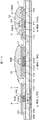
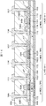
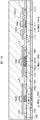
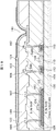
- 画素が形成された表示領域を有する基板を含む表示装置であって、
前記画素は酸化物半導体を用いた第1のTFTを含み、
前記第1のTFTのドレインには第1のポリシリコンが形成され、
前記第1のTFTのソースには第2のポリシリコンが形成され、
前記第1のポリシリコンは、前記第1のTFTを覆う絶縁膜に形成された第1のスルーホールを介して第1の電極と接続し、
前記第2のポリシリコンは、前記第1のTFTを覆う絶縁膜に形成された第2のスルーホールを介して第2の電極と接続していることを特徴とする表示装置。 - 前記基板は、前記表示領域の外側に駆動回路を含み、前記駆動回路はポリシリコンによる第2のTFTを含むことを特徴とする請求項1に記載の表示装置。
- 前記第1のTFTは、n−MOS TFTであることを特徴とする請求項1に記載の表示装置。
- 前記第2のTFTは、n−MOS TFTとp−MOS TFTを含むことを特徴とする請求項2に記載の表示装置。
- 前記表示領域は、さらに、第2のTFTを有することを特徴とする請求項1に記載の表示装置。
- 前記駆動回路は、さらに、第1のTFTを含むことを特徴とする請求項2に記載の表示装置。
- 前記表示装置は液晶表示装置であることを特徴とする請求項1乃至6のいずれか1項に記載の表示装置。
- 前記表示装置は有機EL表示装置であることを特徴とする請求項1乃至6のいずれか1項に記載の表示装置。
- 画素が形成された表示領域を有する基板を含む表示装置であって、
前記画素は酸化物半導体を用いた第1のTFTを含み、
前記第1のTFTのドレインには第1のポリシリコンが形成され、
前記第1のTFTのソースには第2のポリシリコンが形成され、
前記第1のポリシリコンは、前記第1のTFTを覆う絶縁膜に形成された第1のスルーホールを介して第1の電極と接続し、
前記第2のポリシリコンは、前記第2のTFTを覆う絶縁膜に形成された第2のスルーホールを介して第2の電極と接続しており、
前記第1のLTPSと前記酸化物半導体はpn接合をしているか、
前記第2のLTPSと前記酸化物半導体はpn接合していることを特徴とする表示領域。 - 前記基板は、前記表示領域の外側に駆動回路を含み、前記駆動回路はポリシリコンによる第2のTFTを含むことを特徴とする請求項9に記載の表示装置。
- 前記第1のTFTは、n−MOS TFTであることを特徴とする請求項9に記載の表示装置。
- 前記第2のTFTは、n−MOS TFTとp−MOS TFTを含むことを特徴とする請求項10に記載の表示装置。
- 前記表示領域は、さらに、第2のTFTを有することを特徴とする請求項9に記載の表示装置。
- 前記駆動回路は、さらに、第1のTFTを含むことを特徴とする請求項10に記載の表示装置。
- 前記表示装置は液晶表示装置であることを特徴とする請求項9乃至14のいずれか1項に記載の表示装置。
- 前記表示装置は有機EL表示装置であることを特徴とする請求項9乃至14のいずれか1項に記載の表示装置。
Priority Applications (4)
| Application Number | Priority Date | Filing Date | Title |
|---|---|---|---|
| JP2016093071A JP6668160B2 (ja) | 2016-05-06 | 2016-05-06 | 表示装置の製造方法 |
| US15/479,392 US20170323906A1 (en) | 2016-05-06 | 2017-04-05 | Display device |
| CN201710267224.2A CN107346083B (zh) | 2016-05-06 | 2017-04-21 | 显示装置 |
| US16/004,546 US10361229B2 (en) | 2016-05-06 | 2018-06-11 | Display device |
Applications Claiming Priority (1)
| Application Number | Priority Date | Filing Date | Title |
|---|---|---|---|
| JP2016093071A JP6668160B2 (ja) | 2016-05-06 | 2016-05-06 | 表示装置の製造方法 |
Publications (3)
| Publication Number | Publication Date |
|---|---|
| JP2017201665A true JP2017201665A (ja) | 2017-11-09 |
| JP2017201665A5 JP2017201665A5 (ja) | 2019-04-25 |
| JP6668160B2 JP6668160B2 (ja) | 2020-03-18 |
Family
ID=60244133
Family Applications (1)
| Application Number | Title | Priority Date | Filing Date |
|---|---|---|---|
| JP2016093071A Active JP6668160B2 (ja) | 2016-05-06 | 2016-05-06 | 表示装置の製造方法 |
Country Status (3)
| Country | Link |
|---|---|
| US (2) | US20170323906A1 (ja) |
| JP (1) | JP6668160B2 (ja) |
| CN (1) | CN107346083B (ja) |
Cited By (4)
| Publication number | Priority date | Publication date | Assignee | Title |
|---|---|---|---|---|
| JP2020205402A (ja) * | 2019-06-14 | 2020-12-24 | Tianma Japan株式会社 | 薄膜デバイス |
| WO2022009017A1 (ja) * | 2020-07-09 | 2022-01-13 | 株式会社半導体エネルギー研究所 | 表示装置および電子機器 |
| WO2024154255A1 (ja) * | 2023-01-18 | 2024-07-25 | シャープディスプレイテクノロジー株式会社 | 表示装置 |
| US12610690B2 (en) | 2022-08-31 | 2026-04-21 | Lg Display Co., Ltd. | Display apparatus with a thin film transistor having resistances of source and drain regions lower than a resistance of a channel region |
Families Citing this family (6)
| Publication number | Priority date | Publication date | Assignee | Title |
|---|---|---|---|---|
| CN105742297B (zh) * | 2016-04-13 | 2019-09-24 | 深圳市华星光电技术有限公司 | 薄膜晶体管阵列面板及其制作方法 |
| KR102458660B1 (ko) | 2016-08-03 | 2022-10-26 | 가부시키가이샤 한도오따이 에네루기 켄큐쇼 | 표시 장치 및 전자 기기 |
| TWI699892B (zh) * | 2018-09-21 | 2020-07-21 | 友達光電股份有限公司 | 電子裝置及其製造方法 |
| EP3907761B1 (en) * | 2019-01-03 | 2025-11-05 | BOE Technology Group Co., Ltd. | Display backboard and manufacturing method therefor, display panel, and display device |
| CN109904173B (zh) * | 2019-01-11 | 2021-08-06 | 惠科股份有限公司 | 一种显示面板、显示面板的制造方法和显示装置 |
| CN110620120B (zh) * | 2019-09-25 | 2022-07-29 | 福州京东方光电科技有限公司 | 阵列基板及其制作方法、显示装置 |
Citations (6)
| Publication number | Priority date | Publication date | Assignee | Title |
|---|---|---|---|---|
| JPH0491480A (ja) * | 1990-08-03 | 1992-03-24 | Hitachi Ltd | 半導体装置 |
| JP2000312007A (ja) * | 1999-02-23 | 2000-11-07 | Semiconductor Energy Lab Co Ltd | 半導体装置およびその作製方法 |
| JP2010003910A (ja) * | 2008-06-20 | 2010-01-07 | Toshiba Mobile Display Co Ltd | 表示素子 |
| WO2012176422A1 (ja) * | 2011-06-24 | 2012-12-27 | シャープ株式会社 | 表示装置及びその製造方法 |
| WO2013187173A1 (ja) * | 2012-06-15 | 2013-12-19 | ソニー株式会社 | 表示装置、半導体装置および表示装置の製造方法 |
| US20150108454A1 (en) * | 2013-10-17 | 2015-04-23 | Samsung Display Co., Ltd. | Thin film transistor array substrate, organic light-emitting display apparatus, and method of manufacturing the thin film transistor array substrate |
Family Cites Families (9)
| Publication number | Priority date | Publication date | Assignee | Title |
|---|---|---|---|---|
| CN105612608B (zh) * | 2013-10-09 | 2019-12-20 | 夏普株式会社 | 半导体装置及其制造方法 |
| US9214508B2 (en) * | 2014-02-24 | 2015-12-15 | Lg Display Co., Ltd. | Thin film transistor substrate with intermediate insulating layer and display using the same |
| US9721973B2 (en) * | 2014-02-24 | 2017-08-01 | Lg Display Co., Ltd. | Thin film transistor substrate and display using the same |
| EP2911199B1 (en) * | 2014-02-24 | 2020-05-06 | LG Display Co., Ltd. | Thin film transistor substrate and display using the same |
| US20170125452A1 (en) * | 2014-06-17 | 2017-05-04 | Sharp Kabushiki Kaisha | Semiconductor device |
| KR102298336B1 (ko) * | 2014-06-20 | 2021-09-08 | 엘지디스플레이 주식회사 | 유기발광다이오드 표시장치 |
| US9685469B2 (en) * | 2015-04-03 | 2017-06-20 | Apple Inc. | Display with semiconducting oxide and polysilicon transistors |
| US9911762B2 (en) | 2015-12-03 | 2018-03-06 | Innolux Corporation | Display device |
| JP2018125340A (ja) * | 2017-01-30 | 2018-08-09 | 株式会社ジャパンディスプレイ | 表示装置 |
-
2016
- 2016-05-06 JP JP2016093071A patent/JP6668160B2/ja active Active
-
2017
- 2017-04-05 US US15/479,392 patent/US20170323906A1/en not_active Abandoned
- 2017-04-21 CN CN201710267224.2A patent/CN107346083B/zh active Active
-
2018
- 2018-06-11 US US16/004,546 patent/US10361229B2/en active Active
Patent Citations (6)
| Publication number | Priority date | Publication date | Assignee | Title |
|---|---|---|---|---|
| JPH0491480A (ja) * | 1990-08-03 | 1992-03-24 | Hitachi Ltd | 半導体装置 |
| JP2000312007A (ja) * | 1999-02-23 | 2000-11-07 | Semiconductor Energy Lab Co Ltd | 半導体装置およびその作製方法 |
| JP2010003910A (ja) * | 2008-06-20 | 2010-01-07 | Toshiba Mobile Display Co Ltd | 表示素子 |
| WO2012176422A1 (ja) * | 2011-06-24 | 2012-12-27 | シャープ株式会社 | 表示装置及びその製造方法 |
| WO2013187173A1 (ja) * | 2012-06-15 | 2013-12-19 | ソニー株式会社 | 表示装置、半導体装置および表示装置の製造方法 |
| US20150108454A1 (en) * | 2013-10-17 | 2015-04-23 | Samsung Display Co., Ltd. | Thin film transistor array substrate, organic light-emitting display apparatus, and method of manufacturing the thin film transistor array substrate |
Cited By (7)
| Publication number | Priority date | Publication date | Assignee | Title |
|---|---|---|---|---|
| JP2020205402A (ja) * | 2019-06-14 | 2020-12-24 | Tianma Japan株式会社 | 薄膜デバイス |
| JP7464400B2 (ja) | 2019-06-14 | 2024-04-09 | Tianma Japan株式会社 | 薄膜デバイス |
| WO2022009017A1 (ja) * | 2020-07-09 | 2022-01-13 | 株式会社半導体エネルギー研究所 | 表示装置および電子機器 |
| JPWO2022009017A1 (ja) * | 2020-07-09 | 2022-01-13 | ||
| JP7682886B2 (ja) | 2020-07-09 | 2025-05-26 | 株式会社半導体エネルギー研究所 | 表示装置 |
| US12610690B2 (en) | 2022-08-31 | 2026-04-21 | Lg Display Co., Ltd. | Display apparatus with a thin film transistor having resistances of source and drain regions lower than a resistance of a channel region |
| WO2024154255A1 (ja) * | 2023-01-18 | 2024-07-25 | シャープディスプレイテクノロジー株式会社 | 表示装置 |
Also Published As
| Publication number | Publication date |
|---|---|
| US20170323906A1 (en) | 2017-11-09 |
| JP6668160B2 (ja) | 2020-03-18 |
| CN107346083B (zh) | 2020-10-30 |
| CN107346083A (zh) | 2017-11-14 |
| US10361229B2 (en) | 2019-07-23 |
| US20180294286A1 (en) | 2018-10-11 |
Similar Documents
| Publication | Publication Date | Title |
|---|---|---|
| JP6668160B2 (ja) | 表示装置の製造方法 | |
| JP6725317B2 (ja) | 表示装置 | |
| US10459304B2 (en) | Display device | |
| CN111587453B (zh) | 显示装置 | |
| CN207381400U (zh) | 显示装置 | |
| KR101113394B1 (ko) | 액정표시장치의 어레이 기판 | |
| CN207216226U (zh) | 显示装置 | |
| TWI418038B (zh) | 顯示裝置 | |
| US9324735B2 (en) | Array substrate and manufacturing method thereof, display panel and display device | |
| US20080083927A1 (en) | Display device and method of manufacturing the same | |
| WO2020021938A1 (ja) | 表示装置 | |
| KR20130110490A (ko) | 어레이 기판 및 이의 제조 방법 | |
| US20170184893A1 (en) | Semiconductor apparatus, method of manufacturing same, and liquid crystal display apparatus | |
| JP2019040026A (ja) | 表示装置 | |
| JP5475250B2 (ja) | 半導体装置の製造方法及び半導体装置 | |
| US9018623B2 (en) | Array substrate, display panel having the same and method of manufacturing the array substrate | |
| JP2008218626A (ja) | Tftアレイ基板及びその製造方法 | |
| JP2018064020A (ja) | 表示装置 | |
| JP2020181985A (ja) | 表示装置 | |
| KR102142477B1 (ko) | 어레이 기판 및 이의 제조방법 | |
| JP2009158871A (ja) | 表示装置 | |
| JP2008122504A (ja) | 表示装置とその製造方法 | |
| JP2011108706A (ja) | 表示装置 | |
| JP2008263059A (ja) | 半導体装置、その製造方法、及び表示装置 | |
| KR20060117669A (ko) | 박막 트랜지스터 및 박막 트랜지스터 표시판의 제조 방법 |
Legal Events
| Date | Code | Title | Description |
|---|---|---|---|
| A521 | Request for written amendment filed |
Free format text: JAPANESE INTERMEDIATE CODE: A523 Effective date: 20190311 |
|
| A621 | Written request for application examination |
Free format text: JAPANESE INTERMEDIATE CODE: A621 Effective date: 20190311 |
|
| A977 | Report on retrieval |
Free format text: JAPANESE INTERMEDIATE CODE: A971007 Effective date: 20200127 |
|
| TRDD | Decision of grant or rejection written | ||
| A01 | Written decision to grant a patent or to grant a registration (utility model) |
Free format text: JAPANESE INTERMEDIATE CODE: A01 Effective date: 20200204 |
|
| A61 | First payment of annual fees (during grant procedure) |
Free format text: JAPANESE INTERMEDIATE CODE: A61 Effective date: 20200226 |
|
| R150 | Certificate of patent or registration of utility model |
Ref document number: 6668160 Country of ref document: JP Free format text: JAPANESE INTERMEDIATE CODE: R150 |
|
| R250 | Receipt of annual fees |
Free format text: JAPANESE INTERMEDIATE CODE: R250 |
|
| R250 | Receipt of annual fees |
Free format text: JAPANESE INTERMEDIATE CODE: R250 |
|
| R250 | Receipt of annual fees |
Free format text: JAPANESE INTERMEDIATE CODE: R250 |
|
| S111 | Request for change of ownership or part of ownership |
Free format text: JAPANESE INTERMEDIATE CODE: R313113 |
|
| R350 | Written notification of registration of transfer |
Free format text: JAPANESE INTERMEDIATE CODE: R350 |
|
| R250 | Receipt of annual fees |
Free format text: JAPANESE INTERMEDIATE CODE: R250 |