JP2017201732A - 回路基板及びその製造方法 - Google Patents
回路基板及びその製造方法 Download PDFInfo
- Publication number
- JP2017201732A JP2017201732A JP2017159850A JP2017159850A JP2017201732A JP 2017201732 A JP2017201732 A JP 2017201732A JP 2017159850 A JP2017159850 A JP 2017159850A JP 2017159850 A JP2017159850 A JP 2017159850A JP 2017201732 A JP2017201732 A JP 2017201732A
- Authority
- JP
- Japan
- Prior art keywords
- circuit board
- reinforcing member
- reinforcing
- insulating material
- circuit
- Prior art date
- Legal status (The legal status is an assumption and is not a legal conclusion. Google has not performed a legal analysis and makes no representation as to the accuracy of the status listed.)
- Granted
Links
- 238000004519 manufacturing process Methods 0.000 title claims abstract description 13
- 239000000758 substrate Substances 0.000 claims abstract description 99
- 229920005989 resin Polymers 0.000 claims abstract description 74
- 239000011347 resin Substances 0.000 claims abstract description 74
- 239000000463 material Substances 0.000 claims abstract description 51
- 230000002787 reinforcement Effects 0.000 claims abstract description 10
- 229910052751 metal Inorganic materials 0.000 claims abstract description 8
- 239000002184 metal Substances 0.000 claims abstract description 8
- 230000003014 reinforcing effect Effects 0.000 claims description 113
- 239000011810 insulating material Substances 0.000 claims description 53
- 238000003475 lamination Methods 0.000 claims 1
- 238000000576 coating method Methods 0.000 abstract description 2
- 239000011248 coating agent Substances 0.000 abstract 1
- 239000010410 layer Substances 0.000 description 91
- 230000002093 peripheral effect Effects 0.000 description 24
- 238000000034 method Methods 0.000 description 19
- 239000011162 core material Substances 0.000 description 8
- 239000011229 interlayer Substances 0.000 description 8
- 239000010949 copper Substances 0.000 description 6
- RYGMFSIKBFXOCR-UHFFFAOYSA-N Copper Chemical compound [Cu] RYGMFSIKBFXOCR-UHFFFAOYSA-N 0.000 description 5
- 229910052802 copper Inorganic materials 0.000 description 5
- 239000004642 Polyimide Substances 0.000 description 3
- 229910052782 aluminium Inorganic materials 0.000 description 3
- XAGFODPZIPBFFR-UHFFFAOYSA-N aluminium Chemical compound [Al] XAGFODPZIPBFFR-UHFFFAOYSA-N 0.000 description 3
- 238000005452 bending Methods 0.000 description 3
- 230000015572 biosynthetic process Effects 0.000 description 3
- 230000008859 change Effects 0.000 description 3
- 239000000470 constituent Substances 0.000 description 3
- 239000000945 filler Substances 0.000 description 3
- 238000003384 imaging method Methods 0.000 description 3
- 239000007769 metal material Substances 0.000 description 3
- 238000012986 modification Methods 0.000 description 3
- 230000004048 modification Effects 0.000 description 3
- 229920001721 polyimide Polymers 0.000 description 3
- 239000004593 Epoxy Substances 0.000 description 2
- 238000010521 absorption reaction Methods 0.000 description 2
- 230000001133 acceleration Effects 0.000 description 2
- 238000011161 development Methods 0.000 description 2
- 229920002457 flexible plastic Polymers 0.000 description 2
- 239000011521 glass Substances 0.000 description 2
- 239000002985 plastic film Substances 0.000 description 2
- 238000007747 plating Methods 0.000 description 2
- 239000011241 protective layer Substances 0.000 description 2
- 239000004065 semiconductor Substances 0.000 description 2
- 239000002356 single layer Substances 0.000 description 2
- 229920003002 synthetic resin Polymers 0.000 description 2
- 239000000057 synthetic resin Substances 0.000 description 2
- XLYOFNOQVPJJNP-UHFFFAOYSA-N water Substances O XLYOFNOQVPJJNP-UHFFFAOYSA-N 0.000 description 2
- 229920000106 Liquid crystal polymer Polymers 0.000 description 1
- 239000004977 Liquid-crystal polymers (LCPs) Substances 0.000 description 1
- 239000012790 adhesive layer Substances 0.000 description 1
- 239000003990 capacitor Substances 0.000 description 1
- 238000004891 communication Methods 0.000 description 1
- 230000000295 complement effect Effects 0.000 description 1
- 239000002131 composite material Substances 0.000 description 1
- 239000004020 conductor Substances 0.000 description 1
- 238000005520 cutting process Methods 0.000 description 1
- 230000005611 electricity Effects 0.000 description 1
- 239000003822 epoxy resin Substances 0.000 description 1
- 238000005530 etching Methods 0.000 description 1
- 239000004744 fabric Substances 0.000 description 1
- 239000003365 glass fiber Substances 0.000 description 1
- 238000009413 insulation Methods 0.000 description 1
- 238000005304 joining Methods 0.000 description 1
- 238000010030 laminating Methods 0.000 description 1
- 238000003754 machining Methods 0.000 description 1
- 230000003287 optical effect Effects 0.000 description 1
- 239000002245 particle Substances 0.000 description 1
- 230000000149 penetrating effect Effects 0.000 description 1
- 239000005011 phenolic resin Substances 0.000 description 1
- 229920000647 polyepoxide Polymers 0.000 description 1
- -1 polyethylene terephthalate Polymers 0.000 description 1
- 229920000139 polyethylene terephthalate Polymers 0.000 description 1
- 239000005020 polyethylene terephthalate Substances 0.000 description 1
- 230000008569 process Effects 0.000 description 1
- 238000012545 processing Methods 0.000 description 1
- 238000004080 punching Methods 0.000 description 1
- 230000009467 reduction Effects 0.000 description 1
- 238000007789 sealing Methods 0.000 description 1
- 229910000679 solder Inorganic materials 0.000 description 1
- 230000008961 swelling Effects 0.000 description 1
- 229920001187 thermosetting polymer Polymers 0.000 description 1
- 238000012546 transfer Methods 0.000 description 1
Images


Classifications
-
- H—ELECTRICITY
- H05—ELECTRIC TECHNIQUES NOT OTHERWISE PROVIDED FOR
- H05K—PRINTED CIRCUITS; CASINGS OR CONSTRUCTIONAL DETAILS OF ELECTRIC APPARATUS; MANUFACTURE OF ASSEMBLAGES OF ELECTRICAL COMPONENTS
- H05K1/00—Printed circuits
- H05K1/02—Details
- H05K1/14—Structural association of two or more printed circuits
- H05K1/147—Structural association of two or more printed circuits at least one of the printed circuits being bent or folded, e.g. by using a flexible printed circuit
-
- H—ELECTRICITY
- H05—ELECTRIC TECHNIQUES NOT OTHERWISE PROVIDED FOR
- H05K—PRINTED CIRCUITS; CASINGS OR CONSTRUCTIONAL DETAILS OF ELECTRIC APPARATUS; MANUFACTURE OF ASSEMBLAGES OF ELECTRICAL COMPONENTS
- H05K3/00—Apparatus or processes for manufacturing printed circuits
- H05K3/36—Assembling printed circuits with other printed circuits
- H05K3/361—Assembling flexible printed circuits with other printed circuits
-
- H—ELECTRICITY
- H05—ELECTRIC TECHNIQUES NOT OTHERWISE PROVIDED FOR
- H05K—PRINTED CIRCUITS; CASINGS OR CONSTRUCTIONAL DETAILS OF ELECTRIC APPARATUS; MANUFACTURE OF ASSEMBLAGES OF ELECTRICAL COMPONENTS
- H05K2201/00—Indexing scheme relating to printed circuits covered by H05K1/00
- H05K2201/20—Details of printed circuits not provided for in H05K2201/01 - H05K2201/10
- H05K2201/2009—Reinforced areas, e.g. for a specific part of a flexible printed circuit
Landscapes
- Engineering & Computer Science (AREA)
- Microelectronics & Electronic Packaging (AREA)
- Manufacturing & Machinery (AREA)
- Production Of Multi-Layered Print Wiring Board (AREA)
- Structure Of Printed Boards (AREA)
- Structures For Mounting Electric Components On Printed Circuit Boards (AREA)
Abstract
【解決手段】本発明の一形態に係る回路基板は、可撓性配線基材と、補強部とを具備する。上記可撓性配線基材は、第1の端部と、上記第1の端部とは反対側の第2の端部とを有する。上記補強部は、上記第1の端部を選択的に被覆する樹脂層と、上記樹脂層に設けられ上記可撓性配線基材に電気的に接続される回路部と、上記回路部と電気的に接続され、上記樹脂基板に埋設された金属製の板状または枠状の補強部材とを有する。
【選択図】図2
Description
上記可撓性配線基材は、第1の端部と、上記第1の端部とは反対側の第2の端部とを有する。
上記補強部は、上記第1の端部を選択的に被覆する樹脂層と、上記樹脂層に設けられ上記可撓性配線基材に電気的に接続される回路部と、上記回路部と電気的に接続され、記樹脂基板に埋設された金属製の板状または枠状の補強部材とを有する。
上記凹部に金属製の板状又は枠状の補強部材が収容される。
上記一端部に、上記可撓性配線基材および上記補強部材と電気的に接続される回路部が形成される。
図1は、本発明の一実施形態に係る回路基板の構成を示す概略平面図である。図2は、図1におけるA−A線方向断面図である。
なお、各図においてX軸、Y軸及びZ軸は、相互に直交する3軸方向を示しており、Z軸方向は、回路基板の厚み方向に相当する。
本実施形態の回路基板100は、第1の基板本体10と、第2の基板本体20とを有する。回路基板100は、典型的には、制御基板30と一体的に構成されるが、制御基板30とは別部品として構成されてもよい。
第1の基板本体10は、第2の基板本体20と制御基板30との間を接続する可撓性配線基材11で構成され、回路基板100においてフレキシブル部を構成する。可撓性配線基材11は、典型的には、X軸方向に長手方向、Y軸方向に幅方向を有し、長手方向の一端部(第1の端部11a)には補強部12が設けられ、他端部(第2の端部11b)には制御基板30が設けられる。
第2の基板本体20は、可撓性配線基材11の第1の端部11aを選択的に被覆する樹脂層21と、樹脂層21に設けられた回路部22と、第1の端部11aに埋設された金属製の補強部材23とを有する補強部12を含む。第2の基板本体20(あるいは補強部12)は、回路基板100においてリジッド部を構成する。
制御基板30は、IC等の集積回路やその周辺部品等が搭載されるメイン基板に相当し、第1の基板本体10を介して第2の基板本体20と電気的に接続される。制御基板30は、典型的には、第2の基板本体20よりも大面積の両面基板で構成される。
続いて、以上のように構成される回路基板100の製造方法について説明する。
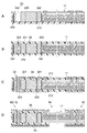
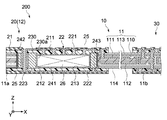
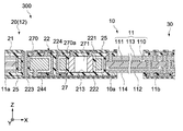
図5は、本発明の他の実施形態に係る回路基板200の構成を示す概略側断面図である。以下、第1の実施形態と異なる構成について主に説明し、第1の実施形態と同様の構成については同様の符号を付しその説明を省略または簡略化する。
図6は、本発明の他の実施形態に係る回路基板300の構成を示す概略側断面図である。以下、第1の実施形態と異なる構成について主に説明し、第1の実施形態と同様の構成については同様の符号を付しその説明を省略または簡略化する。
11…可撓性配線基材
12…補強部
20…第2の基板本体
21…樹脂層
22…回路部
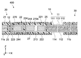
23,230,270…補強部材
230a,270a,270b…キャビティ
26,271…電子部品
30…制御基板
100,200,300,400…回路基板
213…収容部
241…第1の絶縁材
242…第2の絶縁材
400…回路モジュール
E1,E2…素子
Claims (11)
- 第1の端部と、前記第1の端部とは反対側の第2の端部とを有する可撓性配線基材と、
前記第1の端部を選択的に被覆する樹脂層と、前記樹脂層に設けられ前記可撓性配線基材に電気的に接続される回路部と、前記回路部と電気的に接続され、前記第1の端部に埋設された金属製の板状または枠状の補強部材とを有する補強部と
を具備する回路基板。 - 請求項1に記載の回路基板であって、
前記第1の端部は、有底又は無底の凹部を有し、
前記補強部材は、前記凹部に配置される
回路基板 - 請求項2に記載の回路基板であって、
前記補強部の平面形状は矩形であり、
前記補強部材は、面内に溝又はキャビティを有する矩形の板材で構成される
回路基板。 - 請求項3に記載の回路基板であって、
前記キャビティに配置された電子部品をさらに具備する
回路基板。 - 請求項3又は4に記載の回路基板であって、
前記補強部は、前記凹部に配置された前記補強部材の前記溝又はキャビティに充填された第1の絶縁材をさらに有し、
前記第1の絶縁材は、前記樹脂層を構成する樹脂材料よりも熱膨張係数が小さく、かつ、弾性率が高い材料で構成される
回路基板。 - 請求項5に記載の回路基板であって、
前記補強部は、前記凹部と前記補強部材との間の少なくとも前記第2の端部側の一端部に設けられた第2の絶縁材をさらに有し、
前記第2の絶縁材は、前記樹脂層を構成する樹脂材料よりも弾性率が低い材料で構成される
回路基板。 - 請求項6に記載の回路基板であって、
前記補強部は、前記凹部と前記補強部材との間の前記一端部に、前記第1の絶縁材と前記第2の絶縁材との積層部を有する
回路基板。 - 請求項4に記載の回路基板であって、
前記補強部は、前記補強部材の両面を被覆する絶縁層と、前記絶縁層に設けられ前記電子部品及び前記回路部各々に電気的に接続される配線層とをさらに有する
回路基板。 - 請求項1〜8のいずれか1つに記載の回路基板であって、
前記第2の端部に支持され、前記可撓性配線基材と電気的に接続される制御基板をさらに具備する
回路基板。 - 請求項3に記載の回路基板であって、
前記補強部は、前記補強部材の両面を被覆する絶縁層と、前記絶縁層に設けられ前記回路部に電気的に接続される配線層とをさらに有する
回路基板。 - 可撓性配線基材の一端部に凹部を形成し、
前記凹部に金属製の板状又は枠状の補強部材を配置し、
前記一端部に、前記可撓性配線基材および前記補強部材と電気的に接続される回路部を形成する
回路基板の製造方法。
Applications Claiming Priority (2)
| Application Number | Priority Date | Filing Date | Title |
|---|---|---|---|
| JP2016030606 | 2016-02-22 | ||
| JP2016030606 | 2016-02-22 |
Related Parent Applications (1)
| Application Number | Title | Priority Date | Filing Date |
|---|---|---|---|
| JP2017025046A Division JP6281000B2 (ja) | 2016-02-22 | 2017-02-14 | 回路基板及びその製造方法 |
Publications (2)
| Publication Number | Publication Date |
|---|---|
| JP2017201732A true JP2017201732A (ja) | 2017-11-09 |
| JP6281016B2 JP6281016B2 (ja) | 2018-02-14 |
Family
ID=59675692
Family Applications (4)
| Application Number | Title | Priority Date | Filing Date |
|---|---|---|---|
| JP2017025046A Expired - Fee Related JP6281000B2 (ja) | 2016-02-22 | 2017-02-14 | 回路基板及びその製造方法 |
| JP2017159850A Expired - Fee Related JP6281016B2 (ja) | 2016-02-22 | 2017-08-23 | 回路基板及びその製造方法 |
| JP2017234027A Expired - Fee Related JP6800132B2 (ja) | 2016-02-22 | 2017-12-06 | 回路基板及び回路モジュール |
| JP2017234026A Expired - Fee Related JP6822940B2 (ja) | 2016-02-22 | 2017-12-06 | 回路基板 |
Family Applications Before (1)
| Application Number | Title | Priority Date | Filing Date |
|---|---|---|---|
| JP2017025046A Expired - Fee Related JP6281000B2 (ja) | 2016-02-22 | 2017-02-14 | 回路基板及びその製造方法 |
Family Applications After (2)
| Application Number | Title | Priority Date | Filing Date |
|---|---|---|---|
| JP2017234027A Expired - Fee Related JP6800132B2 (ja) | 2016-02-22 | 2017-12-06 | 回路基板及び回路モジュール |
| JP2017234026A Expired - Fee Related JP6822940B2 (ja) | 2016-02-22 | 2017-12-06 | 回路基板 |
Country Status (2)
| Country | Link |
|---|---|
| JP (4) | JP6281000B2 (ja) |
| CN (1) | CN107105570B (ja) |
Families Citing this family (14)
| Publication number | Priority date | Publication date | Assignee | Title |
|---|---|---|---|---|
| CN110800101B (zh) | 2017-06-30 | 2023-09-15 | 株式会社村田制作所 | 电子部件模块 |
| JP6745770B2 (ja) * | 2017-08-22 | 2020-08-26 | 太陽誘電株式会社 | 回路基板 |
| JP6783724B2 (ja) * | 2017-08-22 | 2020-11-11 | 太陽誘電株式会社 | 回路基板 |
| JP2019067873A (ja) * | 2017-09-29 | 2019-04-25 | 太陽誘電株式会社 | 回路基板及び回路モジュール |
| JP6800125B2 (ja) | 2017-09-29 | 2020-12-16 | 太陽誘電株式会社 | 回路基板及び回路モジュール |
| KR102550170B1 (ko) * | 2018-01-04 | 2023-07-03 | 삼성전기주식회사 | 인쇄회로기판 및 이를 포함하는 카메라 모듈 |
| JP2019153668A (ja) * | 2018-03-02 | 2019-09-12 | 太陽誘電株式会社 | 回路基板及びその製造方法 |
| JP2019175977A (ja) * | 2018-03-28 | 2019-10-10 | 太陽誘電株式会社 | 回路基板 |
| JP2020009879A (ja) * | 2018-07-06 | 2020-01-16 | 太陽誘電株式会社 | 回路基板および回路モジュール |
| KR20200102729A (ko) * | 2019-02-22 | 2020-09-01 | 삼성전기주식회사 | 인쇄회로기판 및 이를 구비한 카메라 모듈 |
| CN112366369B (zh) | 2019-07-23 | 2025-07-18 | Sk新能源株式会社 | 感测组件、感测组件的制造方法及电池模块 |
| JP7514086B2 (ja) * | 2020-03-03 | 2024-07-10 | 日東電工株式会社 | 配線回路基板支持アセンブリ |
| CN115361779B (zh) * | 2022-08-26 | 2024-09-13 | 宁波华远电子科技有限公司 | 内埋式元器件的硬质封装结构及其制备方法 |
| CN115565890B (zh) * | 2022-12-07 | 2023-04-18 | 西北工业大学 | 一种折叠式多芯片柔性集成封装方法及柔性集成封装芯片 |
Citations (8)
| Publication number | Priority date | Publication date | Assignee | Title |
|---|---|---|---|---|
| JPS5932191A (ja) * | 1982-08-18 | 1984-02-21 | イビデン株式会社 | プリント配線基板とその製造方法 |
| JP2007273654A (ja) * | 2006-03-31 | 2007-10-18 | Sumitomo Bakelite Co Ltd | フレキシブル回路基板、フレキシブル回路基板の製造方法および電子機器 |
| JP2010114434A (ja) * | 2008-10-08 | 2010-05-20 | Ngk Spark Plug Co Ltd | 部品内蔵配線基板及びその製造方法 |
| JP2010272563A (ja) * | 2009-05-19 | 2010-12-02 | Dainippon Printing Co Ltd | 部品内蔵配線板、部品内蔵配線板の製造方法 |
| JP2012134272A (ja) * | 2010-12-21 | 2012-07-12 | Nec Corp | 部品内蔵モジュール及びこれを備える電子機器並びに部品内蔵モジュールの製造方法 |
| JP2014154941A (ja) * | 2013-02-05 | 2014-08-25 | Taiyo Yuden Co Ltd | モジュール |
| WO2014203603A1 (ja) * | 2013-06-18 | 2014-12-24 | 株式会社村田製作所 | 樹脂多層基板の製造方法 |
| WO2015166588A1 (ja) * | 2014-05-02 | 2015-11-05 | 株式会社メイコー | 部品内蔵リジッドフレックス基板 |
Family Cites Families (5)
| Publication number | Priority date | Publication date | Assignee | Title |
|---|---|---|---|---|
| JP4477844B2 (ja) * | 2003-09-09 | 2010-06-09 | 富士フイルム株式会社 | 撮像モジュールおよびその作成方法 |
| JP2006222182A (ja) * | 2005-02-09 | 2006-08-24 | Shin Kobe Electric Mach Co Ltd | リジッドフレキシブル基板 |
| KR20060098689A (ko) * | 2005-03-03 | 2006-09-19 | 엘지전자 주식회사 | 티씨피 모듈의 그라운드 강화 설계 구조 |
| JP2010286777A (ja) * | 2009-06-15 | 2010-12-24 | Toshiba Corp | 光電気配線フィルム及び光電気配線モジュール |
| KR101482404B1 (ko) * | 2013-05-27 | 2015-01-13 | 삼성전기주식회사 | 리지드 플렉시블 인쇄회로기판 및 그 제조방법 |
-
2017
- 2017-02-14 JP JP2017025046A patent/JP6281000B2/ja not_active Expired - Fee Related
- 2017-02-22 CN CN201710096136.0A patent/CN107105570B/zh not_active Expired - Fee Related
- 2017-08-23 JP JP2017159850A patent/JP6281016B2/ja not_active Expired - Fee Related
- 2017-12-06 JP JP2017234027A patent/JP6800132B2/ja not_active Expired - Fee Related
- 2017-12-06 JP JP2017234026A patent/JP6822940B2/ja not_active Expired - Fee Related
Patent Citations (8)
| Publication number | Priority date | Publication date | Assignee | Title |
|---|---|---|---|---|
| JPS5932191A (ja) * | 1982-08-18 | 1984-02-21 | イビデン株式会社 | プリント配線基板とその製造方法 |
| JP2007273654A (ja) * | 2006-03-31 | 2007-10-18 | Sumitomo Bakelite Co Ltd | フレキシブル回路基板、フレキシブル回路基板の製造方法および電子機器 |
| JP2010114434A (ja) * | 2008-10-08 | 2010-05-20 | Ngk Spark Plug Co Ltd | 部品内蔵配線基板及びその製造方法 |
| JP2010272563A (ja) * | 2009-05-19 | 2010-12-02 | Dainippon Printing Co Ltd | 部品内蔵配線板、部品内蔵配線板の製造方法 |
| JP2012134272A (ja) * | 2010-12-21 | 2012-07-12 | Nec Corp | 部品内蔵モジュール及びこれを備える電子機器並びに部品内蔵モジュールの製造方法 |
| JP2014154941A (ja) * | 2013-02-05 | 2014-08-25 | Taiyo Yuden Co Ltd | モジュール |
| WO2014203603A1 (ja) * | 2013-06-18 | 2014-12-24 | 株式会社村田製作所 | 樹脂多層基板の製造方法 |
| WO2015166588A1 (ja) * | 2014-05-02 | 2015-11-05 | 株式会社メイコー | 部品内蔵リジッドフレックス基板 |
Also Published As
| Publication number | Publication date |
|---|---|
| JP2018046298A (ja) | 2018-03-22 |
| JP6800132B2 (ja) | 2020-12-16 |
| JP6822940B2 (ja) | 2021-01-27 |
| JP6281016B2 (ja) | 2018-02-14 |
| CN107105570A (zh) | 2017-08-29 |
| JP2018046297A (ja) | 2018-03-22 |
| CN107105570B (zh) | 2019-07-23 |
| JP2017152692A (ja) | 2017-08-31 |
| JP6281000B2 (ja) | 2018-02-14 |
Similar Documents
| Publication | Publication Date | Title |
|---|---|---|
| JP6281016B2 (ja) | 回路基板及びその製造方法 | |
| JP6745770B2 (ja) | 回路基板 | |
| JP5093353B2 (ja) | 部品内蔵モジュールの製造方法及び部品内蔵モジュール | |
| US11239170B2 (en) | Stacked modules | |
| US10742855B2 (en) | Circuit board and circuit module | |
| JP6783724B2 (ja) | 回路基板 | |
| CN204335177U (zh) | 电子元器件内置模块 | |
| JP6107941B2 (ja) | 複合基板 | |
| KR20150008771A (ko) | 전자소자 내장형 인쇄회로기판 및 그 제조방법 | |
| KR20150035251A (ko) | 외부접속단자부와 외부접속단자부를 갖는 반도체 패키지 및 그들의 제조방법 | |
| KR101701380B1 (ko) | 소자 내장형 연성회로기판 및 이의 제조방법 | |
| JP5462450B2 (ja) | 部品内蔵プリント配線板及び部品内蔵プリント配線板の製造方法 | |
| KR101139084B1 (ko) | 다층 프린트 기판 및 그 제조 방법 | |
| KR101394964B1 (ko) | 반도체 패키지 및 그 제조 방법 | |
| KR102518174B1 (ko) | 전자 소자 모듈 | |
| US10050014B2 (en) | Circuit substrate and method of manufacturing same | |
| JP6644743B2 (ja) | 回路基板及び半導体モジュール | |
| US10602608B2 (en) | Circuit board | |
| CN112492777B (zh) | 电路板及其制作方法 | |
| CN205356811U (zh) | 电子装置 | |
| KR20110018683A (ko) | 임베디드 회로 기판 및 임베디드 회로 기판의 제조 방법 |
Legal Events
| Date | Code | Title | Description |
|---|---|---|---|
| A621 | Written request for application examination |
Free format text: JAPANESE INTERMEDIATE CODE: A621 Effective date: 20170823 |
|
| A871 | Explanation of circumstances concerning accelerated examination |
Free format text: JAPANESE INTERMEDIATE CODE: A871 Effective date: 20170823 |
|
| A975 | Report on accelerated examination |
Free format text: JAPANESE INTERMEDIATE CODE: A971005 Effective date: 20170829 |
|
| A131 | Notification of reasons for refusal |
Free format text: JAPANESE INTERMEDIATE CODE: A131 Effective date: 20170912 |
|
| A521 | Request for written amendment filed |
Free format text: JAPANESE INTERMEDIATE CODE: A523 Effective date: 20171011 |
|
| A131 | Notification of reasons for refusal |
Free format text: JAPANESE INTERMEDIATE CODE: A131 Effective date: 20171107 |
|
| A521 | Request for written amendment filed |
Free format text: JAPANESE INTERMEDIATE CODE: A523 Effective date: 20171206 |
|
| TRDD | Decision of grant or rejection written | ||
| A01 | Written decision to grant a patent or to grant a registration (utility model) |
Free format text: JAPANESE INTERMEDIATE CODE: A01 Effective date: 20171226 |
|
| A61 | First payment of annual fees (during grant procedure) |
Free format text: JAPANESE INTERMEDIATE CODE: A61 Effective date: 20180122 |
|
| R150 | Certificate of patent or registration of utility model |
Ref document number: 6281016 Country of ref document: JP Free format text: JAPANESE INTERMEDIATE CODE: R150 |
|
| R250 | Receipt of annual fees |
Free format text: JAPANESE INTERMEDIATE CODE: R250 |
|
| LAPS | Cancellation because of no payment of annual fees |