JP2017502173A - モルホリン浴、及び層を化学的に析出させるための方法 - Google Patents
モルホリン浴、及び層を化学的に析出させるための方法 Download PDFInfo
- Publication number
- JP2017502173A JP2017502173A JP2016538718A JP2016538718A JP2017502173A JP 2017502173 A JP2017502173 A JP 2017502173A JP 2016538718 A JP2016538718 A JP 2016538718A JP 2016538718 A JP2016538718 A JP 2016538718A JP 2017502173 A JP2017502173 A JP 2017502173A
- Authority
- JP
- Japan
- Prior art keywords
- bath
- metal
- layer
- sulfur
- morpholine
- Prior art date
- Legal status (The legal status is an assumption and is not a legal conclusion. Google has not performed a legal analysis and makes no representation as to the accuracy of the status listed.)
- Granted
Links
Images



Classifications
-
- C—CHEMISTRY; METALLURGY
- C23—COATING METALLIC MATERIAL; COATING MATERIAL WITH METALLIC MATERIAL; CHEMICAL SURFACE TREATMENT; DIFFUSION TREATMENT OF METALLIC MATERIAL; COATING BY VACUUM EVAPORATION, BY SPUTTERING, BY ION IMPLANTATION OR BY CHEMICAL VAPOUR DEPOSITION, IN GENERAL; INHIBITING CORROSION OF METALLIC MATERIAL OR INCRUSTATION IN GENERAL
- C23C—COATING METALLIC MATERIAL; COATING MATERIAL WITH METALLIC MATERIAL; SURFACE TREATMENT OF METALLIC MATERIAL BY DIFFUSION INTO THE SURFACE, BY CHEMICAL CONVERSION OR SUBSTITUTION; COATING BY VACUUM EVAPORATION, BY SPUTTERING, BY ION IMPLANTATION OR BY CHEMICAL VAPOUR DEPOSITION, IN GENERAL
- C23C18/00—Chemical coating by decomposition of either liquid compounds or solutions of the coating forming compounds, without leaving reaction products of surface material in the coating; Contact plating
- C23C18/02—Chemical coating by decomposition of either liquid compounds or solutions of the coating forming compounds, without leaving reaction products of surface material in the coating; Contact plating by thermal decomposition
- C23C18/12—Chemical coating by decomposition of either liquid compounds or solutions of the coating forming compounds, without leaving reaction products of surface material in the coating; Contact plating by thermal decomposition characterised by the deposition of inorganic material other than metallic material
- C23C18/1204—Chemical coating by decomposition of either liquid compounds or solutions of the coating forming compounds, without leaving reaction products of surface material in the coating; Contact plating by thermal decomposition characterised by the deposition of inorganic material other than metallic material inorganic material, e.g. non-oxide and non-metallic such as sulfides, nitrides based compounds
-
- C—CHEMISTRY; METALLURGY
- C23—COATING METALLIC MATERIAL; COATING MATERIAL WITH METALLIC MATERIAL; CHEMICAL SURFACE TREATMENT; DIFFUSION TREATMENT OF METALLIC MATERIAL; COATING BY VACUUM EVAPORATION, BY SPUTTERING, BY ION IMPLANTATION OR BY CHEMICAL VAPOUR DEPOSITION, IN GENERAL; INHIBITING CORROSION OF METALLIC MATERIAL OR INCRUSTATION IN GENERAL
- C23C—COATING METALLIC MATERIAL; COATING MATERIAL WITH METALLIC MATERIAL; SURFACE TREATMENT OF METALLIC MATERIAL BY DIFFUSION INTO THE SURFACE, BY CHEMICAL CONVERSION OR SUBSTITUTION; COATING BY VACUUM EVAPORATION, BY SPUTTERING, BY ION IMPLANTATION OR BY CHEMICAL VAPOUR DEPOSITION, IN GENERAL
- C23C2/00—Hot-dipping or immersion processes for applying the coating material in the molten state without affecting the shape; Apparatus therefor
- C23C2/04—Hot-dipping or immersion processes for applying the coating material in the molten state without affecting the shape; Apparatus therefor characterised by the coating material
-
- C—CHEMISTRY; METALLURGY
- C23—COATING METALLIC MATERIAL; COATING MATERIAL WITH METALLIC MATERIAL; CHEMICAL SURFACE TREATMENT; DIFFUSION TREATMENT OF METALLIC MATERIAL; COATING BY VACUUM EVAPORATION, BY SPUTTERING, BY ION IMPLANTATION OR BY CHEMICAL VAPOUR DEPOSITION, IN GENERAL; INHIBITING CORROSION OF METALLIC MATERIAL OR INCRUSTATION IN GENERAL
- C23C—COATING METALLIC MATERIAL; COATING MATERIAL WITH METALLIC MATERIAL; SURFACE TREATMENT OF METALLIC MATERIAL BY DIFFUSION INTO THE SURFACE, BY CHEMICAL CONVERSION OR SUBSTITUTION; COATING BY VACUUM EVAPORATION, BY SPUTTERING, BY ION IMPLANTATION OR BY CHEMICAL VAPOUR DEPOSITION, IN GENERAL
- C23C18/00—Chemical coating by decomposition of either liquid compounds or solutions of the coating forming compounds, without leaving reaction products of surface material in the coating; Contact plating
- C23C18/02—Chemical coating by decomposition of either liquid compounds or solutions of the coating forming compounds, without leaving reaction products of surface material in the coating; Contact plating by thermal decomposition
- C23C18/12—Chemical coating by decomposition of either liquid compounds or solutions of the coating forming compounds, without leaving reaction products of surface material in the coating; Contact plating by thermal decomposition characterised by the deposition of inorganic material other than metallic material
- C23C18/1204—Chemical coating by decomposition of either liquid compounds or solutions of the coating forming compounds, without leaving reaction products of surface material in the coating; Contact plating by thermal decomposition characterised by the deposition of inorganic material other than metallic material inorganic material, e.g. non-oxide and non-metallic such as sulfides, nitrides based compounds
- C23C18/1208—Oxides, e.g. ceramics
- C23C18/1216—Metal oxides
-
- H—ELECTRICITY
- H10—SEMICONDUCTOR DEVICES; ELECTRIC SOLID-STATE DEVICES NOT OTHERWISE PROVIDED FOR
- H10F—INORGANIC SEMICONDUCTOR DEVICES SENSITIVE TO INFRARED RADIATION, LIGHT, ELECTROMAGNETIC RADIATION OF SHORTER WAVELENGTH OR CORPUSCULAR RADIATION
- H10F71/00—Manufacture or treatment of devices covered by this subclass
-
- H—ELECTRICITY
- H10—SEMICONDUCTOR DEVICES; ELECTRIC SOLID-STATE DEVICES NOT OTHERWISE PROVIDED FOR
- H10F—INORGANIC SEMICONDUCTOR DEVICES SENSITIVE TO INFRARED RADIATION, LIGHT, ELECTROMAGNETIC RADIATION OF SHORTER WAVELENGTH OR CORPUSCULAR RADIATION
- H10F77/00—Constructional details of devices covered by this subclass
- H10F77/10—Semiconductor bodies
- H10F77/12—Active materials
- H10F77/126—Active materials comprising only Group I-III-VI chalcopyrite materials, e.g. CuInSe2, CuGaSe2 or CuInGaSe2 [CIGS]
-
- H—ELECTRICITY
- H10—SEMICONDUCTOR DEVICES; ELECTRIC SOLID-STATE DEVICES NOT OTHERWISE PROVIDED FOR
- H10F—INORGANIC SEMICONDUCTOR DEVICES SENSITIVE TO INFRARED RADIATION, LIGHT, ELECTROMAGNETIC RADIATION OF SHORTER WAVELENGTH OR CORPUSCULAR RADIATION
- H10F77/00—Constructional details of devices covered by this subclass
- H10F77/10—Semiconductor bodies
- H10F77/12—Active materials
- H10F77/128—Active materials comprising only Group I-II-IV-VI kesterite materials, e.g. Cu2ZnSnSe4 or Cu2ZnSnS4
-
- Y—GENERAL TAGGING OF NEW TECHNOLOGICAL DEVELOPMENTS; GENERAL TAGGING OF CROSS-SECTIONAL TECHNOLOGIES SPANNING OVER SEVERAL SECTIONS OF THE IPC; TECHNICAL SUBJECTS COVERED BY FORMER USPC CROSS-REFERENCE ART COLLECTIONS [XRACs] AND DIGESTS
- Y02—TECHNOLOGIES OR APPLICATIONS FOR MITIGATION OR ADAPTATION AGAINST CLIMATE CHANGE
- Y02E—REDUCTION OF GREENHOUSE GAS [GHG] EMISSIONS, RELATED TO ENERGY GENERATION, TRANSMISSION OR DISTRIBUTION
- Y02E10/00—Energy generation through renewable energy sources
- Y02E10/50—Photovoltaic [PV] energy
- Y02E10/541—CuInSe2 material PV cells
Landscapes
- Chemical & Material Sciences (AREA)
- Engineering & Computer Science (AREA)
- Organic Chemistry (AREA)
- Materials Engineering (AREA)
- Mechanical Engineering (AREA)
- Metallurgy (AREA)
- Chemical Kinetics & Catalysis (AREA)
- Inorganic Chemistry (AREA)
- Physics & Mathematics (AREA)
- Thermal Sciences (AREA)
- General Chemical & Material Sciences (AREA)
- Ceramic Engineering (AREA)
- Photovoltaic Devices (AREA)
- Chemically Coating (AREA)
- Chemical Vapour Deposition (AREA)
Abstract
Description
− 周期表のIIB及びIIIA族の少なくとも1種の元素の中から選択される金属を含む金属塩と、
− 硫黄前駆体と
を含む。この浴は、モルホリン化合物をさらに含む。
− 周期表のIIB及びIIIA族の少なくとも1種の元素の中から選択される金属を含む金属塩と、
− 硫黄前駆体と
を含む浴において、少なくとも金属及び硫黄をベースとする層を、化学的に析出させるための方法にも関する。

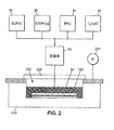
101 基板
102 裏面金属接点
103 吸収体層
104 バッファ層
105 第1窓層
106 前面電気接点
10 金属塩を含む第1の水溶液
20 硫黄前駆体を含む第2の水溶液
30 アンモニア
40 過硫酸塩系無機添加剤を含む第4の水溶液
50 溶液(反応混合物)
200 チャンバ
210 水浴
220 カバー
230 モータ
400 デバイス
Claims (16)
- 少なくとも金属及び硫黄をベースとする層(104)を析出させるための化学浴であって、溶液(50)中に、
− 周期表のIIB及びIIIA族の少なくとも1種の元素の中から選択される金属を含む金属塩(10)と、
− 硫黄前駆体(20)と
を含み、
モルホリン化合物(40)をさらに含むことを特徴とする浴。 - 前記モルホリン化合物は、錯化剤として前記浴において作用するアミン基及びエーテル基を有している、請求項1に記載の浴。
- 前記化合物(40)が、化学式C4H9NOである、請求項1または2に記載の浴。
- 0.05mol/Lと1mol/Lの間の硫黄化合物(20)の濃度に対して、0.001mol/Lと10mol/Lの間の濃度のモルホリン(40)が浴に提供されている、請求項1から3のいずれか一項に記載の浴。
- 前記金属塩(10)を含む溶液が、0.01mol/Lと1mol/Lの間の濃度の硫酸亜鉛、酢酸亜鉛、及び塩化亜鉛の中から選択される溶液である、請求項4に記載の浴。
- 10mol/L未満の濃度で、アンモニア溶液(30)をさらに含む、請求項4又は5に記載の浴。
- アンモニア溶液を含まない、請求項1から5のいずれか一項に記載の浴。
- 前記硫黄化合物(20)を含む溶液が、チオ尿素CS(NH2)2の溶液である、請求項1から7のいずれか一項に記載の浴。
- 前記金属がIIB族の元素である、請求項1から8のいずれか一項に記載の浴。
- 前記金属が亜鉛である、請求項9に記載の浴。
- 溶液(50)中に、
− 周期表のIIB及びIIIA族の少なくとも1種の元素の中から選択される金属を含む金属塩(10)と、
− 硫黄前駆体(20)と
を含む浴において、少なくとも金属及び硫黄をベースとする層(104)を化学的に析出させるための方法であって、
モルホリン化合物(40)が前記浴にさらに提供されることを特徴とする前記方法。 - 前記層(104)が金属硫化物をベースとする、請求項11に記載の方法。
- 前記層(104)が金属オキシ硫化物をベースとする、請求項11に記載の方法。
- 析出の間の前記浴の温度が40℃と100℃の間である、請求項11から13のいずれか一項に記載の方法。
- 金属及び硫黄をベースとする前記層(104)が、光起電力特性を有する層の上に析出され、光起電力特性を有する前記層が、薄膜ソーラーセルの吸収体を形成している、請求項11から14のいずれか一項に記載の方法。
- 前記吸収体が、Cu(In,Ga)(S,Se)2、Cu2(Zn,Sn)(S,Se)4、及びそれらの誘導体の中のカルコパイライト型化合物をベースとする、請求項15に記載の析出方法。
Applications Claiming Priority (2)
| Application Number | Priority Date | Filing Date | Title |
|---|---|---|---|
| FR1362539A FR3014909B1 (fr) | 2013-12-12 | 2013-12-12 | Bain a morpholine et procede pour le depot chimique d'une couche. |
| PCT/FR2015/050350 WO2015087022A1 (fr) | 2013-12-12 | 2015-02-12 | Bain à morpholine et procédé pour le dépôt chimique d'une couche |
Publications (2)
| Publication Number | Publication Date |
|---|---|
| JP2017502173A true JP2017502173A (ja) | 2017-01-19 |
| JP6169283B2 JP6169283B2 (ja) | 2017-07-26 |
Family
ID=50289929
Family Applications (1)
| Application Number | Title | Priority Date | Filing Date |
|---|---|---|---|
| JP2016538718A Active JP6169283B2 (ja) | 2013-12-12 | 2015-02-12 | モルホリン浴、及び層を化学的に析出させるための方法 |
Country Status (6)
| Country | Link |
|---|---|
| US (1) | US20160312347A1 (ja) |
| EP (1) | EP3080334B1 (ja) |
| JP (1) | JP6169283B2 (ja) |
| FR (1) | FR3014909B1 (ja) |
| TW (1) | TW201527592A (ja) |
| WO (1) | WO2015087022A1 (ja) |
Families Citing this family (1)
| Publication number | Priority date | Publication date | Assignee | Title |
|---|---|---|---|---|
| TWI583017B (zh) * | 2015-11-27 | 2017-05-11 | 賴志煌 | 薄膜太陽能電池的製作方法 |
Citations (3)
| Publication number | Priority date | Publication date | Assignee | Title |
|---|---|---|---|---|
| JP2008510310A (ja) * | 2004-08-18 | 2008-04-03 | ハーン−マイトネル−インスチツート ベルリン ゲゼルシャフト ミット ベシュレンクテル ハフツング | 半導体基板、特に黄銅鉱薄膜太陽電池の吸収層上に硫化亜鉛バッファ層を化学浴析出により施与する方法 |
| US20130084401A1 (en) * | 2010-01-28 | 2013-04-04 | Manz Cigs Technology Gmbh | Bath Deposition Solution for the Wet-Chemical Deposition of a Metal Sulfide Layer and Related Production Method |
| JP2013512306A (ja) * | 2009-11-25 | 2013-04-11 | イー・アイ・デュポン・ドウ・ヌムール・アンド・カンパニー | CZTS/Se前駆体インクとCZTS/Se薄フィルムおよびCZTS/Se系光電池の製造方法 |
Family Cites Families (3)
| Publication number | Priority date | Publication date | Assignee | Title |
|---|---|---|---|---|
| US3630763A (en) * | 1969-03-21 | 1971-12-28 | Chapman Chem Co | Control of transit stain on wood products |
| US6454846B2 (en) * | 2000-02-23 | 2002-09-24 | Seiko Epson Corporation | Ink composition suitable for use in ink jet recording |
| US7306663B2 (en) * | 2003-08-05 | 2007-12-11 | Halox, Division Of Hammond Group, Inc. | Corrosion inhibitor |
-
2013
- 2013-12-12 FR FR1362539A patent/FR3014909B1/fr active Active
-
2014
- 2014-12-12 TW TW103143576A patent/TW201527592A/zh unknown
-
2015
- 2015-02-12 WO PCT/FR2015/050350 patent/WO2015087022A1/fr not_active Ceased
- 2015-02-12 EP EP15706911.3A patent/EP3080334B1/fr active Active
- 2015-02-12 JP JP2016538718A patent/JP6169283B2/ja active Active
- 2015-02-12 US US15/103,694 patent/US20160312347A1/en not_active Abandoned
Patent Citations (3)
| Publication number | Priority date | Publication date | Assignee | Title |
|---|---|---|---|---|
| JP2008510310A (ja) * | 2004-08-18 | 2008-04-03 | ハーン−マイトネル−インスチツート ベルリン ゲゼルシャフト ミット ベシュレンクテル ハフツング | 半導体基板、特に黄銅鉱薄膜太陽電池の吸収層上に硫化亜鉛バッファ層を化学浴析出により施与する方法 |
| JP2013512306A (ja) * | 2009-11-25 | 2013-04-11 | イー・アイ・デュポン・ドウ・ヌムール・アンド・カンパニー | CZTS/Se前駆体インクとCZTS/Se薄フィルムおよびCZTS/Se系光電池の製造方法 |
| US20130084401A1 (en) * | 2010-01-28 | 2013-04-04 | Manz Cigs Technology Gmbh | Bath Deposition Solution for the Wet-Chemical Deposition of a Metal Sulfide Layer and Related Production Method |
Also Published As
| Publication number | Publication date |
|---|---|
| EP3080334B1 (fr) | 2021-09-22 |
| US20160312347A1 (en) | 2016-10-27 |
| EP3080334A1 (fr) | 2016-10-19 |
| WO2015087022A1 (fr) | 2015-06-18 |
| WO2015087022A8 (fr) | 2015-11-12 |
| FR3014909A1 (fr) | 2015-06-19 |
| FR3014909B1 (fr) | 2016-01-29 |
| JP6169283B2 (ja) | 2017-07-26 |
| TW201527592A (zh) | 2015-07-16 |
Similar Documents
| Publication | Publication Date | Title |
|---|---|---|
| Romanyuk et al. | All solution‐processed chalcogenide solar cells–from single functional layers towards a 13.8% efficient CIGS device | |
| Li et al. | Phase-selective synthesis of Cu2ZnSnS4 nanocrystals using different sulfur precursors | |
| Wang et al. | Fabrication of a Cu2ZnSn (S, Se) 4 photovoltaic device by a low-toxicity ethanol solution process | |
| Wu et al. | Polytypic nanocrystals of Cu-based ternary chalcogenides: colloidal synthesis and photoelectrochemical properties | |
| US20140220728A1 (en) | Methods of forming semiconductor films including i2-ii-iv-vi4 and i2-(ii,iv)-iv-vi4 semiconductor films and electronic devices including the semiconductor films | |
| Asokan | Solar cells of Cu 2 ZnSnS 4 thin films prepared by chemical bath deposition method | |
| Shi et al. | Kesterite-based next generation high performance thin film solar cell: current progress and future prospects | |
| Seo et al. | Effect of sulfur and copper amounts in sol–gel precursor solution on the growth, crystal properties, and optical properties of Cu2ZnSnS4 films | |
| Khot et al. | Novel-approach for fabrication of CdS thin films for photoelectrochemical solar cell application | |
| JP5564688B2 (ja) | Czts系半導体用cbd溶液、czts系半導体用バッファ層の製造方法及び光電素子 | |
| Saha | A Status Review on Cu2ZnSn (S, Se) 4‐Based Thin‐Film Solar Cells | |
| JP4549570B2 (ja) | ヘテロ接合薄膜太陽電池の製造方法 | |
| Ullah et al. | Electrodeposition of CuGaSe2 and CuGaS2 thin films for photovoltaic applications | |
| Patil et al. | Investigating the Role of Selenium-Ion Concentration on Optoelectronic Properties of the Cu2ZnSn (S1–x Se x) 4 Thin Films | |
| Kauk-Kuusik et al. | Cu 2 ZnSnS 4 monograin layer solar cells for flexible photovoltaic applications | |
| Mkawi et al. | Solution-processed sphere-like Cu2ZnSnS4 nanoparticles for solar cells: effect of oleylamine concentration on properties | |
| Shafi et al. | Optimization of electrodeposition time on the properties of Cu2ZnSnS4 thin films for thin film solar cell applications | |
| JP6035122B2 (ja) | 光電変換素子および光電変換素子のバッファ層の製造方法 | |
| Banu et al. | Analysis of sulphur deficiency defect prevalent in SILAR-CdS films | |
| JP6169283B2 (ja) | モルホリン浴、及び層を化学的に析出させるための方法 | |
| Gopinath et al. | Growth of polycrystalline In2S3 thin films by chemical bath deposition using acetic acid as a complexing agent for solar cell application | |
| Laghchim et al. | Experimental and simulation study for an improved efficiency of 8.46% of a CTS thin-film solar cell: impact of tin (Sn) concentration on structural, optoelectronic properties and photovoltaic performance | |
| Seo et al. | Control of metal salt ratio and MoS2 layer thickness in a Cu2ZnSnS4 thin film solar cell | |
| KR101484156B1 (ko) | 틴이 도핑된 인듐 설파이드 박막의 제조방법 및 이를 버퍼층으로 이용한 cigs 박막태양전지의 제조방법 | |
| Bagade et al. | Synthesis of (CdZn) Se thin films by a facile aqueous phase route and their photoelectrochemical performance for solar cell application |
Legal Events
| Date | Code | Title | Description |
|---|---|---|---|
| A521 | Request for written amendment filed |
Free format text: JAPANESE INTERMEDIATE CODE: A523 Effective date: 20160809 |
|
| A621 | Written request for application examination |
Free format text: JAPANESE INTERMEDIATE CODE: A621 Effective date: 20160809 |
|
| A977 | Report on retrieval |
Free format text: JAPANESE INTERMEDIATE CODE: A971007 Effective date: 20170517 |
|
| TRDD | Decision of grant or rejection written | ||
| A01 | Written decision to grant a patent or to grant a registration (utility model) |
Free format text: JAPANESE INTERMEDIATE CODE: A01 Effective date: 20170529 |
|
| A61 | First payment of annual fees (during grant procedure) |
Free format text: JAPANESE INTERMEDIATE CODE: A61 Effective date: 20170627 |
|
| R150 | Certificate of patent or registration of utility model |
Ref document number: 6169283 Country of ref document: JP Free format text: JAPANESE INTERMEDIATE CODE: R150 |
|
| R250 | Receipt of annual fees |
Free format text: JAPANESE INTERMEDIATE CODE: R250 |
|
| R250 | Receipt of annual fees |
Free format text: JAPANESE INTERMEDIATE CODE: R250 |
|
| R250 | Receipt of annual fees |
Free format text: JAPANESE INTERMEDIATE CODE: R250 |
|
| R250 | Receipt of annual fees |
Free format text: JAPANESE INTERMEDIATE CODE: R250 |
|
| R250 | Receipt of annual fees |
Free format text: JAPANESE INTERMEDIATE CODE: R250 |
|
| R250 | Receipt of annual fees |
Free format text: JAPANESE INTERMEDIATE CODE: R250 |