JP2017526247A - Current sensing circuit using single operational amplifier with DC offset auto-zeroing - Google Patents
Current sensing circuit using single operational amplifier with DC offset auto-zeroing Download PDFInfo
- Publication number
- JP2017526247A JP2017526247A JP2017500914A JP2017500914A JP2017526247A JP 2017526247 A JP2017526247 A JP 2017526247A JP 2017500914 A JP2017500914 A JP 2017500914A JP 2017500914 A JP2017500914 A JP 2017500914A JP 2017526247 A JP2017526247 A JP 2017526247A
- Authority
- JP
- Japan
- Prior art keywords
- circuit
- amplifier
- capacitor
- output
- configuration
- Prior art date
- Legal status (The legal status is an assumption and is not a legal conclusion. Google has not performed a legal analysis and makes no representation as to the accuracy of the status listed.)
- Pending
Links
Images




Classifications
-
- H—ELECTRICITY
- H03—ELECTRONIC CIRCUITRY
- H03F—AMPLIFIERS
- H03F3/00—Amplifiers with only discharge tubes or only semiconductor devices as amplifying elements
- H03F3/005—Amplifiers with only discharge tubes or only semiconductor devices as amplifying elements using switched capacitors, e.g. dynamic amplifiers; using switched capacitors as resistors in differential amplifiers
-
- H—ELECTRICITY
- H03—ELECTRONIC CIRCUITRY
- H03F—AMPLIFIERS
- H03F1/00—Details of amplifiers with only discharge tubes, only semiconductor devices or only unspecified devices as amplifying elements
- H03F1/30—Modifications of amplifiers to reduce influence of variations of temperature or supply voltage or other physical parameters
- H03F1/303—Modifications of amplifiers to reduce influence of variations of temperature or supply voltage or other physical parameters using a switching device
-
- H—ELECTRICITY
- H03—ELECTRONIC CIRCUITRY
- H03F—AMPLIFIERS
- H03F3/00—Amplifiers with only discharge tubes or only semiconductor devices as amplifying elements
- H03F3/45—Differential amplifiers
- H03F3/45071—Differential amplifiers with semiconductor devices only
- H03F3/45076—Differential amplifiers with semiconductor devices only characterised by the way of implementation of the active amplifying circuit in the differential amplifier
- H03F3/45179—Differential amplifiers with semiconductor devices only characterised by the way of implementation of the active amplifying circuit in the differential amplifier using MOSFET transistors as the active amplifying circuit
-
- H—ELECTRICITY
- H03—ELECTRONIC CIRCUITRY
- H03F—AMPLIFIERS
- H03F2200/00—Indexing scheme relating to amplifiers
- H03F2200/231—Indexing scheme relating to amplifiers the input of an amplifier can be switched on or off by a switch to amplify or not an input signal
-
- H—ELECTRICITY
- H03—ELECTRONIC CIRCUITRY
- H03F—AMPLIFIERS
- H03F2203/00—Indexing scheme relating to amplifiers with only discharge tubes or only semiconductor devices as amplifying elements covered by H03F3/00
- H03F2203/45—Indexing scheme relating to differential amplifiers
- H03F2203/45156—At least one capacitor being added at the input of a dif amp
-
- H—ELECTRICITY
- H03—ELECTRONIC CIRCUITRY
- H03K—PULSE TECHNIQUE
- H03K2217/00—Indexing scheme related to electronic switching or gating, i.e. not by contact-making or -breaking covered by H03K17/00
- H03K2217/0027—Measuring means of, e.g. currents through or voltages across the switch
Landscapes
- Engineering & Computer Science (AREA)
- Power Engineering (AREA)
- Amplifiers (AREA)
- Continuous-Control Power Sources That Use Transistors (AREA)
Abstract
DCオフセット感知及び補償を提供すると同時に、連続的な電流感知動作を可能にする、シングルオペアンプDCオフセット自動ゼロ化機能を有する電流感知回路。シングルオペアンプ設計は、第1の位相において、電流感知回路の出力段をドライブするために出力を供給しつつ、DCオフセットを感知及び格納するように動作することができる。シングルオペアンプ設計は、第2の位相において、感知されたDCオフセットを使用して、出力段をドライブすることができ且つ第1の位相において使用されることができる正確な出力を生成するように動作することができる。【選択図】 図4A current sensing circuit having a single operational amplifier DC offset auto-zeroing function that provides continuous offset current sensing while providing DC offset sensing and compensation. The single op amp design can operate to sense and store the DC offset in the first phase while providing an output to drive the output stage of the current sensing circuit. The single op amp design operates in the second phase to use the sensed DC offset to drive the output stage and produce an accurate output that can be used in the first phase. can do. [Selection] Figure 4
Description
[0001]本願は、2014年7月11日に出願された米国特許出願第14/329,615号の優先権を主張し、その内容は、全ての目的で全体として参照によって本明細書に組み込まれる。 [0001] This application claims priority to US patent application Ser. No. 14 / 329,615 filed Jul. 11, 2014, the contents of which are hereby incorporated by reference in their entirety for all purposes. It is.
[0002]別途明記されない限り、前述のものは、本明細書に記載されている本願請求項の先行技術であると認められず、そのように解釈されるべきではない。 [0002] Unless stated otherwise, the foregoing is not to be construed as prior art to the claims set forth herein and should not be construed as such.
[0003]負荷に伝達されている電流量を知ることは、広範囲のアプリケーションにおいて有益であり得る。例えば、低電力電子デバイス(例えば、スマートフォン、コンピュータタブレット及び他の家庭用電化製品)では、バッテリ寿命に対するシステムのインパクトを理解するために、電源電流がモニタリングされ得る。負荷電流はまた、過電流保護回路においてセーフティクリティカル判断を行うために使用され得る。一般に、電流センサは、電流(例えば、負荷を通る電流)を検知し、検知された電流を表す出力電流を生成することができる回路である。幾つかの回路アプリケーションでは、出力電流は、検知された電流に比例する測定しやすい出力電圧に変換されることができる。 [0003] Knowing the amount of current being transferred to a load can be beneficial in a wide range of applications. For example, in low power electronic devices (eg, smartphones, computer tablets and other consumer electronics), the power supply current can be monitored to understand the impact of the system on battery life. The load current can also be used to make safety critical decisions in the overcurrent protection circuit. In general, a current sensor is a circuit that can sense a current (eg, a current through a load) and generate an output current representative of the sensed current. In some circuit applications, the output current can be converted to a measurable output voltage that is proportional to the sensed current.
[0004]典型的な電流感知回路設計では、負荷に電流を供給するパスデバイス(pass device)を流れる電流(感知されている電流)を正確に表す(複製する)センス電流を生成することが可能であることは重要である。パスデバイスを流れる電流のセンス電流を生成することの精度限界の分析は、チャネルの一方端から他方端のレプリカデバイスの電圧降下がパスデバイスのチャネルの一方端から他方端の電圧降下と極めて正確に一致しなければならないことを示している。典型的に、アクティブな高利得フィードバックループが使用され、これは、1つ又は複数の増幅器を用いる。各増幅器におけるオフセットは、正確なセンス電流を生成するために、極めて低い値に低減されるべきである。 [0004] A typical current sensing circuit design can generate a sense current that accurately represents (duplicates) the current flowing through a pass device that supplies current to the load (the current being sensed). It is important to be. An analysis of the accuracy limits of generating the sense current of the current flowing through the pass device has shown that the voltage drop across the channel from one end of the channel to the other end is very accurate with the voltage drop across the pass device channel from one end to the other. Indicates that they must match. Typically, an active high gain feedback loop is used, which uses one or more amplifiers. The offset in each amplifier should be reduced to a very low value in order to generate an accurate sense current.
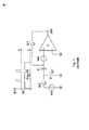
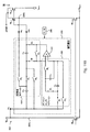
[0005]「自動ゼロ化」と呼ばれる技法は、増幅器のDCオフセットを自動的にゼロにドライブすることができる。自動ゼロ化は、スイッチドキャパシタ技法を使用する。従来のスイッチドキャパシタ自動ゼロ技法は、増幅器が、キャパシタがそのオフセットをサンプルする反復サイクルの一部の間に使用されることを防ぐものである。図1は、例えば、基本的なスイッチドキャパシタ自動ゼロ設計を示す。時間Φ1では、スイッチS1及びS2が閉じており、スイッチS3が開いており、これにより、キャパシタCは、増幅器AのDCオフセットVosを感知及び格納することができる。時間Φ2では、スイッチS1及びS2が開いており、スイッチS3が閉じており、これにより、増幅器Aは、キャパシタCに格納されている電圧を使用して信号x(t)に作用して、増幅器AのDCオフセットをキャンセルすることができる。しかしながら、時間Φ1中、DCオフセットがキャパシタCによって感知されているとき、増幅器Aは、信号x(t)を処理するために使用されることができない。この間欠性は、増幅器Aを使用する回路の性能を劣化させ得る。この欠点を示さない代替例は、各々2つの入力を有する2つのオペアンプを使用する。そのような設計は、従って大きく、より大きなダイ面積を必要とし、より多くの電力を消費する。 [0005] A technique called "auto-zeroing" can automatically drive the amplifier's DC offset to zero. Automatic zeroing uses a switched capacitor technique. Conventional switched capacitor auto-zero techniques prevent the amplifier from being used during a portion of the repetitive cycle in which the capacitor samples its offset. FIG. 1 shows, for example, a basic switched capacitor automatic zero design. At time Φ1, switches S1 and S2 are closed and switch S3 is open so that capacitor C can sense and store the DC offset Vos of amplifier A. At time Φ2, switches S1 and S2 are open and switch S3 is closed, so that amplifier A operates on signal x (t) using the voltage stored in capacitor C, and the amplifier The DC offset of A can be canceled. However, amplifier A cannot be used to process signal x (t) when a DC offset is being sensed by capacitor C during time Φ1. This intermittency can degrade the performance of the circuit using amplifier A. An alternative that does not show this drawback uses two operational amplifiers, each with two inputs. Such a design is therefore large, requires a larger die area and consumes more power.
[0006]実施形態では、回路には、集積器セクション、増幅器セクション及びオフセットヌル化セクションを有する増幅器セクションが含まれる。増幅器セクションは、回路の出力に接続されること又はそれから切断されることができる。増幅器セクションは、オフセットヌル化セクションが増幅器セクションのオフセットを格納しているとき、回路の出力から切断されることができる。集積器セクションは、増幅器セクションが出力から切断されているとき、回路の出力をドライブし、回路の入力において誤差信号を感知することができる。増幅器セクションは、集積器セクションが増幅器セクションに接続されているとき、制御信号を生成するために、回路の出力に接続されることができる。オフセットヌル化セクションは、増幅器セクションのDCオフセットを補償することができる。 [0006] In an embodiment, the circuit includes an amplifier section having an integrator section, an amplifier section, and an offset nulling section. The amplifier section can be connected to or disconnected from the output of the circuit. The amplifier section can be disconnected from the output of the circuit when the offset nulling section stores the amplifier section offset. The integrator section can drive the output of the circuit and sense an error signal at the input of the circuit when the amplifier section is disconnected from the output. The amplifier section can be connected to the output of the circuit to generate a control signal when the integrator section is connected to the amplifier section. The offset nulling section can compensate for the DC offset of the amplifier section.
[0007]幾つかの実施形態では、増幅器セクションは、シングルオペアンプを含む。幾つかの実施形態では、増幅器は、差動モード増幅器である。 [0007] In some embodiments, the amplifier section includes a single operational amplifier. In some embodiments, the amplifier is a differential mode amplifier.
[0008]幾つかの実施形態では、回路は、電流感知回路に接続され得る。 [0008] In some embodiments, the circuit may be connected to a current sensing circuit.
[0009]幾つかの実施形態では、回路は、増幅器セクション、集積器セクション及びオフセットヌル化セクションの間の接続を構成するためのスイッチを含み得る。 [0009] In some embodiments, the circuit may include a switch for configuring a connection between the amplifier section, the integrator section, and the offset nulling section.
[0010]以下の詳細な説明及び添付の図面は、本開示の性質及び利点のより良い理解を与える。 [0010] The following detailed description and the accompanying drawings provide a better understanding of the nature and advantages of the present disclosure.
[0011]以下の説明及び特に図面に関して、示される詳細が、実例となる説明を目的に複数の例を表し、本開示の原理の説明及び概念的な態様を提供するために提示されることが強調される。この点に関して、本開示の根本的な理解に必要とされるものを超える実装形態の詳細を示すための試みは行われない。以下の説明は、図面と併せて、本開示に係る実施形態がどのように実施され得るかを当業者に明らかにする。添付の図面は以下の通りである。 [0011] With the following description and with particular reference to the drawings, the details presented are presented for illustrative purposes and provide a description of the principles and conceptual aspects of the present disclosure for illustrative purposes. To be emphasized. In this regard, no attempt is made to show implementation details beyond what is required for a fundamental understanding of the present disclosure. The following description, in conjunction with the drawings, makes it clear to those skilled in the art how the embodiments according to the present disclosure can be implemented. The attached drawings are as follows.
[0026]以下の説明では、説明の目的で、本開示の完全な理解を与えるために、多数の例及び特定の詳細が示される。しかしながら、特許請求の範囲で明記されている本開示が、これらの例の特徴のうちの幾つか又は全てを、単独で又は以下で説明される他の特徴と組み合わせて含み得ること、及び、本明細書で説明されるこれらの特徴及び概念の変更例又は等価物を更に含み得ることは当業者には明らかになるであろう。 [0026] In the following description, for purposes of explanation, numerous examples and specific details are set forth in order to provide a thorough understanding of the present disclosure. However, the disclosure as defined in the claims may include some or all of these example features, either alone or in combination with other features described below, and It will be apparent to those skilled in the art that modifications or equivalents of these features and concepts described in the specification may be further included.
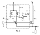
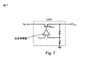
[0027]図2は、本開示に係る、電子回路(図示されない)における電流フローを感知するための電流感知回路200を示す。電流感知回路200は、パスデバイスMpassを通って、制御デバイス14によって制御される負荷12へと流れる電流フローIloadを感知し得る。幾つかの実施形態では、例えば、パスデバイスMpass及び制御デバイス14は、低ドロップアウト(LDO)レギュレータを構成し得る。制御デバイス14は、LDOの誤差増幅器であり得る(例えば、図7参照)。しかしながら、他の実施形態では、パスデバイスMpass及び制御デバイス14が、負荷12をドライブするための任意の適用可能な電子回路の構成要素であることが認識されるだろう。
[0027] FIG. 2 illustrates a
[0028]幾つかの実施形態では、電流感知回路200は、パスデバイスMpassを電流ミラーとして構成された感知デバイスMsenseを備え得る。Mpass及びMsenseの制御入力(例えば、電界効果トランジスタFETのケースではゲート端子)は、制御デバイス14に接続され得、Mpass及びMsenseの出力(例えば、ソース端子)は、負荷に接続され得る。
[0028] In some embodiments, the
[0029]Mpassを通る電流を正確にミラーリングするために、Mpassのチャネル及びMsenseのチャネルの一方端から他方端の電圧降下VDSは一致すべきである。従って、電流感知回路200は、入力ノード208aにおける電圧レベルと一致するようにMsenseの入力ノード208b(例えば、ドレイン端子)における電圧レベルを調整するために、出力段204をドライブするための増幅器段(増幅器回路)202を含む高利得フィードバックループを利用し得る。以下で説明されるように、幾つかの実施形態では、増幅器段202は、タイミング回路206からのタイミング信号に基づいて動作し得る。
[0029] In order to mirror exactly the current through M pass, the voltage drop V DS at the other end from one end of the channel of the channel and M sense of M pass should match. Thus, the
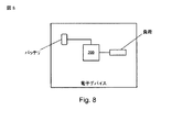
[0030]出力段204は、電流源として動作するFET Mmir1を備え得る。増幅器段202の出力(Out)は、Mmir1を流れる電流量を制御し得る。出力段204は、Mmir1を電流ミラーとして構成されたFET Mmir2を更に備え得る。Mmir2を通る電流フロー(センス電流)Imeasは、負荷電流Iloadを表す。幾つかの実施形態では、Mmir2のサイズは、電流増幅比がImeasに対して適切な信号を生成するように、Mmir1に対して寸法(ゲート幅、ゲート長)が決定され得る。幾つかの実施形態では、電流ミラーMmir1,Mmir2は、電流感知回路200を組み込む電子デバイス(例えば、図8)において生成され得る内部電圧レベルVddを使用してバイアスが掛けられ得る。例えば、図8に例示されるようなバッテリによって動作されるデバイス(例えば、セルラ電話、コンピュータタブレット、等)では、内部電圧Vddは、バッテリからもたらされ得る。幾つかの実施形態では、電流感知回路200は、例えば、バックコンバータ内のスイッチング電力コンバータ(図示されない)の出力を(例えば、バッテリ電圧未満に)副調整する際に使用され得る。
[0030] The
[0031]動作中、増幅器段202は、入力In1,In2間で感知されるノード208a,208bにおける電圧差(誤差)をゼロにドライブするようにフィードバックループにおいてMmir1を調整し得る。負荷電流Iloadが変動すると、In1における電圧も変化するだろう。Mmir1を通る電流は、In2において同じ電圧を供給するように調整され得る。FET Mmir2は、Mmir1を通る電流をミラーリングし、故に、負荷電流Iloadを表すセンス電流Imeasを供給する。本開示に従って、増幅器段202におけるDCオフセットは、Msenseのチャネル及びMpassのチャネルの一方端から他方端の電圧降下VDSの正確な一致を維持するために大幅に低減され得る。増幅器段202の追加の詳細が以下に提供されるだろう。
[0031] In operation,
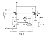
[0032]図2の電流感知回路200は、パスデバイスMpassがNMOSデバイスである設計に適切である。図3を参照すると、パスデバイスMpassがPMOSデバイスである設計において使用され得る電流感知回路300が示される。出力段304は、Msenseをカスコードとして構成されたFET Mcascを備え得る。この実施形態では、Mcascの出力は、センス電流Imeasを生成する。増幅器段202の入力In1,In2は、それぞれMpass及びMsenseのノード308a,308b(例えば、ドレイン端子)に接続され得る。動作中、増幅器段202は、入力In1,In2において感知されるノード208a,208b間の電圧の差分をゼロに低減するようにフィードバックループにおいてMcascを調整する。負荷電流Iloadが変動すると、In1における電圧も変化するだろう。Mcascを通る電流は、ノード308bにおける電圧と同じ電圧がIn2において現れるように調整されるだろう。故に、Mcascから出力される電流は、負荷電流Iloadを表す出力センス電流Imeasを供給する。
[0032] The
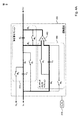
[0033]図4を参照して、本開示に係る、増幅器段202の追加の詳細がここから説明されるだろう。幾つかの実施形態では、増幅器段202は、2つの入力In1,In2及び1つの出力Outを備え得る。増幅器段202内の構成要素は、増幅器セクション(増幅器)402、集積器セクション404及びオフセットヌル化セクション406を含み得る。増幅器402は、反転(−)入力及び非反転(+)入力を有する、従来の2入力演算増幅器(オペアンプ)であり得る。本開示に従って、増幅器402は、シングルオペアンプを備える。
[0033] With reference to FIG. 4, additional details of the
[0034]増幅器段202は、OPEN及びCLOSEという2つの異なる構成を行き来するスイッチΦ1及びΦ2を更に含み得る。幾つかの実施形態では、タイミング回路206(例えば、クロック回路)は、OPEN状態又はCLOSE状態にスイッチを動作するための制御信号Φ1,Φ2を生成し得る。例えば、Φ1によって識別されるスイッチは、制御信号Φ1に従って、OPEN及びCLOSEすることができ、Φ2によって識別されるスイッチは、制御信号Φ2に従ってOPEN及びCLOSEすることができる。幾つかの実施形態では、タイミング回路206は、2つのスイッチ構成を行き来するために2つの制御信号Φ1、Φ2を使用するが、他の実施形態では、タイミング回路が、構成間でスイッチを制御するために追加の信号を使用し得ることは、以下の説明から認識されるだろう。
[0034] The
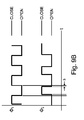
[0035]少しの間図9Aを参照すると、幾つかの実施形態では、制御信号Φ1及びΦ2は、クロックパルスであり得る。各Φ1クロック及びΦ2クロックは、50%デューティサイクルと、互いに対して180度の位相のズレを有し得る。実際、Φ1スイッチ及びΦ2スイッチが同時にCLOSEすることは、回路における短絡及び他の望ましくない回路条件を引き起こす可能性があるため、そうしないことが好ましい。従って、幾つかの実施形態では、Φ1及びΦ2クロックの一方又は両方のデューティサイクルは、Φ1スイッチとΦ2スイッチとの間でブレークビフォアメイク(break-before-make)動作を確実にすべく、僅かな遅延がこれらクロックの立ち下がりエッジと立ち上がりエッジとの間に導入されることができるように調整され得る。例えば、図9Bは、遅延δが、Φ1の立ち下がりエッジとΦ2の立ち上がりエッジの間に、及びΦ1の立ち上がりエッジとΦ2の立ち下がりエッジとの間に導入される、クロックパルスΦ1,Φ2を示す。 [0035] Referring briefly to FIG. 9A, in some embodiments, the control signals Φ1 and Φ2 may be clock pulses. Each Φ1 clock and Φ2 clock may have a 50% duty cycle and a 180 degree phase shift with respect to each other. In fact, it is preferable not to do so because the Φ1 and Φ2 switches CLOSE at the same time can cause short circuits in the circuit and other undesirable circuit conditions. Thus, in some embodiments, the duty cycle of one or both of the Φ1 and Φ2 clocks is slightly increased to ensure a break-before-make operation between the Φ1 and Φ2 switches. Delays can be adjusted so that delays can be introduced between the falling and rising edges of these clocks. For example, FIG. 9B shows clock pulses Φ1, Φ2 in which the delay δ is introduced between the falling edge of Φ1 and the rising edge of Φ2, and between the rising edge of Φ1 and the falling edge of Φ2. .
[0036]続けて図4を参照すると、幾つかの実施形態では、集積器セクション404は、キャパシタ(出力キャパシタ)C2及びキャパシタ(誤差キャパシタ)C3を備え得る。キャパシタC2の片側は、増幅器段202の出力(Out)に接続される。キャパシタC3の片側は、増幅器段202のIn1入力に接続される。スイッチの一構成では、キャパシタC2,C3は、直列に接続され、フィードバックループにおいて増幅器402に接続され得る。スイッチの別の構成では、キャパシタC2,C3及び増幅器420は、共通基準(「仮想接地」)としてIn1入力だけを共有するか、そうでなければ、互いから切断される。
[0036] With continued reference to FIG. 4, in some embodiments, the
[0037]幾つかの実施形態では、オフセットヌル化セクション406は、キャパシタ(オフセットキャパシタ)C1を備え得る。スイッチの一構成では、キャパシタC1は、増幅器402のDCオフセット電圧を感知及び格納するために接続され得る。スイッチの別の構成では、キャパシタC1は、増幅器のDCオフセットを補償するために、格納された電圧を増幅器402に印加するために接続され得る。
[0037] In some embodiments, the offset
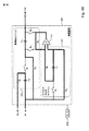
[0038]ここで図4Aを参照して、位相Φ1における増幅器段202の動作が説明されるだろう。スイッチのこの構成でセットアップされる電子経路が太線で示される。位相Φ1において、キャパシタC3は、増幅器402に接続される。増幅器402の出力は、C3に格納された電荷に基づいて、増幅器段202の出力(Out)をドライブするだろう。
[0038] Referring now to FIG. 4A, the operation of
[0039]キャパシタC2が負のフィードバックループにおいて接続されているため、当業者は、増幅器402が、C3に格納される電荷を、C2に既に格納されている電荷に効率的に追加するであろうことを理解するだろう。負のフィードバックループは、C2に格納される電荷の量を、C3の電荷の量に制限するだろう。過度に多い電荷又は過度に少ない電荷をC2に蓄積させるであろう増幅器402におけるDCオフセットは、キャパシタC1によって補償され得、これは、位相Φ2中の増幅器段202の動作の説明からより明らかになるであろう。
[0039] Because capacitor C2 is connected in a negative feedback loop, those skilled in the art will effectively add
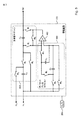
[0040]ここで図4Bを参照すると、位相Φ2における増幅器段202の動作が説明されるだろう。スイッチのこの構成によってセットアップされる電子経路が太線で示される。位相Φ2において、集積器セクション404は、増幅器402から切断され、増幅器402の出力は、増幅器段202の出力(Out)から切断される。図4Aでは、位相Φ1中、キャパシタC2がキャパシタC3を介して増幅器段202のIn1入力を基準とすることに留意されたい。位相Φ2において、C2が依然としてIn1を基準としていることから、キャパシタC2に格納されている電荷は、増幅器段202の出力(Out)をドライブすることができる。故に、位相Φ2において増幅器402は出力Outから切断されるが、出力Outは、依然として、C2によってドライブされることができる。位相Φ2において、C3は、C2から切断され、増幅器段202のIn1入力とIn2入力との間の電位を感知及び格納するためにIn1入力及びIn2入力の間に接続される。
[0040] Referring now to FIG. 4B, the operation of
[0041]位相Φ2において、増幅器402は、直結利得フィードバックで構成される。キャパシタC1は、増幅器402の複数の入力の間に接続され、増幅器段202のIn1入力を基準とする。増幅器402によってC1に格納される電荷は、増幅器のDCオフセットを表す。従って、キャパシタC1は、位相Φ2において増幅器402のDCオフセットをサンプリング及び格納し、それは、次に、上述したように、位相Φ1において、DCオフセットを補償するために使用される。
[0041] In phase Φ2,
[0042]図5を参照すると、幾つかの実施形態では、追加のキャパシタC4が、キャパシタC1と動作するために提供され得る。キャパシタC4は、C1によってサンプリングされたDCオフセットがサンプルごとに変動し得る使用ケースにおいて、このDCオフセットのよりロバストな格納を提供するために、フィルタ処理機能を提供し得る。動作中、位相Φ2においてC1がDCオフセットをサンプリングしているとき、C4は、残りの回路から切断され、C4に蓄積された電荷は何れもC4上に留まる。位相Φ1において、C1及びC4は、並列に接続されており、C1とC4との間での電荷共有が生じる。位相Φ1と位相Φ2との間の多数のサイクルの間に、C1及びC4の間の電圧は、増幅器402のDCオフセットへと次第に増大するだろう。位相Φ2においてC1によって感知されるDCオフセットの変動は、位相Φ1においてC4によって「平滑化」され得る。他の実施形態では、追加のそのようなフィルタ処理キャパシタが提供され得ることが認識されることができる。
[0042] Referring to FIG. 5, in some embodiments, an additional capacitor C4 may be provided to operate with capacitor C1. Capacitor C4 may provide a filtering function to provide a more robust storage of this DC offset in use cases where the DC offset sampled by C1 may vary from sample to sample. In operation, when C1 is sampling the DC offset in phase Φ2, C4 is disconnected from the rest of the circuit and any charge stored in C4 remains on C4. In the phase Φ1, C1 and C4 are connected in parallel, and charge sharing occurs between C1 and C4. During multiple cycles between phase Φ1 and phase Φ2, the voltage between C1 and C4 will gradually increase to the DC offset of
[0043]図6を参照すると、幾つかの実施形態では、増幅器402の非反転入力が、In1入力の代わりに基準電圧Vrefを基準とし得る。この構成は、In1と増幅器402(例えば、VIN)への電源との間の電圧差が過度に小さい特定の使用ケースにおいて適切であり得る。そのような使用ケースの例が図10Aに例示される。増幅器402が適切に動作するためのヘッドルーム要件が存在する。例えば、増幅器402を直結利得フィードバックに配置することは、増幅器の電源がIn1よりも十分大きくない場合、問題である。そのケースでは、増幅器フィードバックループは、正しく動作することができない。図6Aは、増幅器402の非反転入力のための基準として機能するためのIn1入力又は基準電圧Vrefを選択するのにセレクタ602が使用されることができる実施形態を例示する。図6及び6Aは、上述した追加のフィルタ処理キャパシタC4を示す。当然ながら、幾つかの実施形態では、フィルタ処理キャパシタC4が省略されることができることは認識されるだろう。
[0043] Referring to FIG. 6, in some embodiments, the non-inverting input of
[0044]少しの間図2を参照して、本開示に係る電流感知のための基本の動作が、以下に要約され得る。
・キャパシタを用いて、モニタリングされているノード(例えば、208a)と制御ノード(例えば、208b)との間の電位差(誤差)を測定すること。
・集積器を使用してキャパシタ上の電荷を第2のキャパシタ上に集積する。
・誤差をゼロにドライブするために負のフィードバックループにおいて集積器を使用すること。
[0044] Referring briefly to FIG. 2, the basic operation for current sensing according to the present disclosure may be summarized as follows.
• Using a capacitor to measure the potential difference (error) between the monitored node (eg, 208a) and the control node (eg, 208b).
Use the integrator to integrate the charge on the capacitor onto the second capacitor.
Use an integrator in the negative feedback loop to drive the error to zero.
[0045]本開示に係る特定の動作が、以下に要約され得る。
・1つの位相(例えば、Φ2)において、
−オフセットキャパシタ(例えば、C1)上に増幅器のDCオフセットをサンプリングする。
−誤差キャパシタ(例えば、C3)上に誤差をサンプリングする。
−誤差を低減するために出力キャパシタ(例えば、C2)を使用する。
・別の位相(例えば、Φ1)において、
−サンプリングされた誤差を出力キャパシタ上に集積するために増幅器を使用する。
−誤差を低減するために増幅器を使用する。
−DCオフセットを補償するためにオフセットキャパシタを使用する。
[0045] Certain operations according to the present disclosure may be summarized below.
In one phase (for example, Φ2)
Sample the DC offset of the amplifier on the offset capacitor (eg C1).
-Sampling the error on the error capacitor (eg C3).
Use an output capacitor (eg C2) to reduce the error.
In another phase (eg, Φ1)
Use an amplifier to integrate the sampled error onto the output capacitor.
-Use an amplifier to reduce the error.
Use an offset capacitor to compensate for the DC offset.
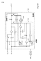
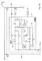
[0046]図10A及び10Bを参照して、図3に示される電流感知回路300の文脈において増幅器段202の動作の説明が、ここから説明されるだろう。図10Aは、フィルタ処理キャパシタC4及び電圧基準Vrefを有する増幅器段202の実施形態を示す。図3に関連して上で説明したように、増幅器段202は、ノード308aと308bとの間の電圧差を感知し、ノード308bにおける電圧をノード308aにおける電圧と等しく保つようにMcascを調整する。図10A及び10Bの構成では、In1がVOUTに接続されているため、回路ヘッドルーム(VINとVOUTとの間の差分)が過度に小さい場合、In1が基準(「仮想接地」)として使用され、VINが増幅器に電源供給するとき、増幅器402のためのヘッドルームは不十分であり得る。従って、図10A及び10Bに示されるように、別個の基準電圧(Vref)が、増幅器402のための十分なヘッドルームを確実にするために提供され得る。
[0046] Referring to FIGS. 10A and 10B, a description of the operation of
[0047]図10Aを参照すると、位相Φ2のための構成であるスイッチが示される。スイッチのこの構成では、キャパシタC3は、In1及びIn2の間に、且つ、ノード308aと308b間の電圧差を感知するために接続されている。従って、C3は、Mpassデバイス及びMsenseデバイスのVDS間の誤差を感知及び格納する。増幅器段202は、Mcascを通る電流フローを維持するために、出力Outに接続されているキャパシタC2を使用してMcascのゲート電圧を「保持」するだろう。故に、増幅器402が、出力Outから切断されていても、Mcascは、依然として、C2上の電荷のおかげで位相Φ2中適切に動作することができる。Mcascを通る電流Imeasは、負荷電流Iloadを表す。出力Outから切断されている増幅器402は、増幅器のDCオフセット電圧をC1に格納するために、直結利得ループにおいてキャパシタC1と接続されることができる。
[0047] Referring to FIG. 10A, a switch that is configured for phase Φ2 is shown. In this configuration of the switch, capacitor C3 is connected between In 1 and In 2 and to sense the voltage difference between
[0048]図10Bを参照すると、スイッチは、位相Φ1のための構成である。この位相では、キャパシタC3上の電圧は、Φ2中に感知されるノード308aと308bとの間の電圧差を格納する。この電圧差は、訂正される必要があるノード308a,308b間の誤差を表す。増幅器402の出力(Out)が、キャパシタC2及びMcascに接続されているため、増幅器は、C3内の電荷をC2上に集積し、同時に、ノード308a,308b間の誤差に従ってMcascを調整することができる。C2に格納される電荷は、DCオフセット感知を行うために増幅器402がMcascから切断されているとき、C2が、Φ2においてMcascのゲート電圧を保持し続けることを可能にする。Φ1中の増幅器402のDCオフセットの補正は、キャパシタC1(そして、幾つかの実施形態ではC4)がC3と直列に接続されているおかげで生じる。この配置は、負荷電流の正確な感知のためにDCオフセット補正が生じることを可能にしつつ、負荷電流感知回路300の連続的なON動作を可能にする。
[0048] Referring to FIG. 10B, the switch is configured for phase Φ1. In this phase, the voltage on capacitor C3 stores the voltage difference between
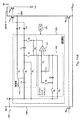
[0049]図11A及び11Bを参照して、図2に示される電流感知回路200の文脈において、増幅器段202の動作の説明が、ここから説明されるだろう。図11Aは、フィルタ処理キャパシタC4を有する増幅器段202の実施形態を示す。図2に関連して上で説明したように、増幅器段202は、ノード208aと208bとの間の電圧差(誤差)を感知し、ノード208bにおける電圧をノード208aにおける電圧と等しく保つようにMmir1を調整する。FET Mmir2は、負荷電流Iloadを表す出力電流Imeasを生成するために、Mmir1を通る電流フローをミラーリングする。
[0049] With reference to FIGS. 11A and 11B, a description of the operation of
[0050]図11Aでは、スイッチは、位相Φ2のための構成である。増幅器402はMmir1から接続されており、よって、Mmir1を制御しないが、FET Mmir1のゲート電圧は、キャパシタC2上の電荷のおかげで動作され続ける。キャパシタC1は、増幅器402のDCオフセットを感知及び格納する。キャパシタC3は、ノード208a,208b間の電圧(誤差)を感知及び格納する。
[0050] In FIG. 11A, the switch is configured for phase Φ2.
[0051]図11Bでは、スイッチは、位相Φ1のための構成になっている。位相Φ2中C3によって感知される誤差は、Mmir1を調整するための信号を生成するために、及び位相Φ2中C2がMmir1のゲート電圧を保持し続けることができるようにC2を充電するために増幅器402によって使用される。増幅器402のDCオフセットは、C1(そして、幾つかの実施形態ではC4)によって補償される。
[0051] In FIG. 11B, the switch is configured for phase Φ1. The error sensed by C3 during phase Φ2 is to generate a signal to adjust M mir1 and to charge C2 so that C2 during phase Φ2 can continue to hold the gate voltage of M mir1. Used by the
[0052]スイッチΦ1及びΦ2の動作からの電荷注入は、キャパシタに格納されている電荷に影響を及ぼすことができ、故に、キャパシタ上の電圧に影響を及ぼし、DCオフセット機能の正確性にインパクトを与えることができる。(コモンモード効果を抑制する)差動回路を使用することによって、電荷注入は、大部分が、コモンモード効果となるように作られ得、故に、大部分は、差動回路によって拒否されるだろう。 [0052] Charge injection from the operation of switches Φ1 and Φ2 can affect the charge stored in the capacitor, thus affecting the voltage on the capacitor and impacting the accuracy of the DC offset function. Can be given. By using a differential circuit (suppressing the common mode effect), charge injection can be made mostly to be a common mode effect, and therefore most will be rejected by the differential circuit. Let's go.
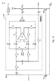
[0053]ここで図12を参照すると、本開示の別の実施形態に係る増幅器段1202は、差動集積器設計を用い得る。差動集積器を使用することは、差動設計の性質により、コモンモード拒否を改善する利益を提供する。図12は、NMOS LDOを示す。しかしながら、差動構成がPMOS LDOに組み込まれ得ることは当業者によって認識されるだろう。
[0053] Referring now to FIG. 12, an
[0054]位相Φ1及び位相Φ2における動作は、前述の実施形態に類似するが、差動の文脈では異なる。差動増幅器A1の差動入力は、対応するキャパシタC1a/C1b及びC2a/C2bを有する。A2は、出力OUTにおいける制御信号へと、A1からの差動出力を変換することができる差動/シングルエンド増幅器/コンバータであり得る。 [0054] The operation in phase Φ1 and phase Φ2 is similar to the previous embodiment, but different in a differential context. The differential input of the differential amplifier A1 has corresponding capacitors C1a / C1b and C2a / C2b. A2 can be a differential / single-ended amplifier / converter that can convert the differential output from A1 to a control signal at output OUT.
[0055]キャパシタC1a及びC1bは、位相Φ2中、差動増幅器A1の差動入力においてDCオフセットを感知及び格納し、位相Φ1中、ヌル化キャパシタとして機能する。キャパシタC3は、Φ2中に感知されるノード308aと308bとの間の電圧差を格納する。キャパシタC3に格納される電荷は、位相Φ1中、キャパシタC2a及びC2bに集積され得、それらは、次に、A2への入力を維持し、そしてOUTにおいて出力を維持するために、位相Φ2中に保持キャパシタとして機能することができる。
[0055] Capacitors C1a and C1b sense and store a DC offset at the differential input of differential amplifier A1 during phase Φ2, and function as nulling capacitors during phase Φ1. Capacitor C3 stores the voltage difference between
利点及び技術的効果
[0056]本開示に係る実施形態は、より正確な電流感知を供給することができる。特定の実施形態では、電流感知における正確性は、感知トランジスタ上への伝送トランジスタの電圧降下のより正確な複製によって達成されることができる。本開示に係る実施形態は、連続したオン動作を提供することができるシングルオペアンプ自動ゼロ化設計を使用して増幅器におけるDCオフセットを低減することができる。
Advantages and technical effects
[0056] Embodiments according to the present disclosure can provide more accurate current sensing. In certain embodiments, accuracy in current sensing can be achieved by more accurate replication of the voltage drop of the transfer transistor over the sensing transistor. Embodiments according to the present disclosure can reduce DC offset in the amplifier using a single op amp auto-zeroing design that can provide continuous on-operation.
[0057]上の説明は、特定の実施形態の態様がどのように実装され得るかについての例とともに、本開示の様々な実施形態を例示する。上の例は、唯一の実施形態であるとみなされるべきではなく、以下の特許請求の範囲によって定義される特定の実施形態の柔軟性及び利点を例示するために提示されている。上の開示と以下の特許請求の範囲に基づいて、他の配置、実施形態、実装、及び等価物が、特許請求の範囲で定義される本開示の範囲から逸脱することなく用いられ得る。 [0057] The above description illustrates various embodiments of the present disclosure, along with examples of how aspects of particular embodiments may be implemented. The above examples should not be considered to be the only embodiments, but are presented to illustrate the flexibility and advantages of certain embodiments as defined by the following claims. Based on the above disclosure and the following claims, other arrangements, embodiments, implementations, and equivalents may be used without departing from the scope of the present disclosure as defined in the claims.
[0058]以下を特許請求する。 [0058] The following are claimed.
Claims (26)
第1の回路入力及び第2の回路入力と、
回路出力と、
第1のキャパシタと、
前記回路出力に接続された第2のキャパシタと、
第1の増幅器入力及び第2の増幅器入力並びに増幅器出力を有する増幅器と、
第1の構成で動作可能であり、第2の構成で動作可能である複数のスイッチと
を備え、
前記スイッチの前記第1の構成では、
前記増幅器出力は、前記回路出力から切断され、
前記第1のキャパシタは、前記増幅器のDCオフセットを感知するために、前記増幅器入力間に接続され、
前記第2のキャパシタは、前記回路出力と前記回路入力のうちの1つとの間にのみ接続され、
前記スイッチの前記第2の構成では、
前記増幅器出力は、前記回路出力に接続され、
前記第1のキャパシタは、前記増幅器の前記DCオフセットを補償するために、前記増幅器入力のうちの1つに接続され、
前記第2のキャパシタは、フィードバックループにおいて前記増幅器に接続される、
回路。 A circuit,
A first circuit input and a second circuit input;
Circuit output,
A first capacitor;
A second capacitor connected to the circuit output;
An amplifier having a first amplifier input and a second amplifier input and an amplifier output;
A plurality of switches operable in the first configuration and operable in the second configuration,
In the first configuration of the switch,
The amplifier output is disconnected from the circuit output;
The first capacitor is connected between the amplifier inputs to sense a DC offset of the amplifier;
The second capacitor is connected only between the circuit output and one of the circuit inputs;
In the second configuration of the switch,
The amplifier output is connected to the circuit output;
The first capacitor is connected to one of the amplifier inputs to compensate for the DC offset of the amplifier;
The second capacitor is connected to the amplifier in a feedback loop;
circuit.
第1の回路入力及び第2の回路入力と、
回路出力と、
出力を有する増幅器と、ここで、前記出力は、前記回路出力に接続されない第1の構成と、前記回路出力に接続される第2の構成とを有し、
前記回路出力に接続された出力キャパシタと、ここで、前記出力キャパシタは、フィードバックループにおいて前記増幅器に接続された第1の構成と、前記増幅器に接続されない第2の構成とを有し、
前記第1の回路入力に接続された入力キャパシタと、前記入力キャパシタは、前記出力キャパシタを有するフィードバックループにおいて前記増幅器に接続された第1の構成と、前記第2の回路入力にのみ接続された第2の構成とを有する、
前記増幅器の第1の入力及び第2の入力に接続された第1の構成を有し、前記入力キャパシタが前記出力キャパシタを有する前記フィードバックループにおいて前記増幅器に接続されたときに、前記入力キャパシタと直列に接続された第2の構成を有する第1のオフセットキャパシタと
を備える回路。 A circuit,
A first circuit input and a second circuit input;
Circuit output,
An amplifier having an output, wherein the output has a first configuration not connected to the circuit output and a second configuration connected to the circuit output;
An output capacitor connected to the circuit output, wherein the output capacitor has a first configuration connected to the amplifier in a feedback loop and a second configuration not connected to the amplifier;
An input capacitor connected to the first circuit input; the input capacitor connected only to the second circuit input; and a first configuration connected to the amplifier in a feedback loop having the output capacitor. A second configuration;
A first configuration connected to a first input and a second input of the amplifier; and when the input capacitor is connected to the amplifier in the feedback loop having the output capacitor; And a first offset capacitor having a second configuration connected in series.
負荷に接続可能な出力端子を有する伝送トランジスタと、
前記伝送トランジスタを通る電流フローをミラーリングするために前記伝送トランジスタに接続された感知トランジスタと、
前記感知トランジスタに接続された出力段と、
前記パストランジスタに接続された第1の回路入力と、前記感知トランジスタに接続された第2の回路入力と、前記出力段に接続された回路出力とを有する増幅器回路と
を備え、前記増幅器回路は、
選択的に、前記回路出力に接続可能又は前記回路出力から切断可能である出力を有する増幅器セクションと、
前記回路出力に接続され、且つ、選択的に、前記増幅器セクションと接続可能又は前記増幅器セクションと切断可能である集積器セクションと、
前記増幅器セクションに接続されたオフセットヌル化セクションと
を備え、
ここにおいて、前記増幅器セクションは、前記オフセットヌル化セクションが前記増幅器のオフセットをサンプリングしているときに、前記回路出力から切断され、
前記集積器セクションは、前記増幅器セクションが前記回路出力から切断されているときに、前記出力段をドライブするために前記回路出力の出力を供給する、
回路。 A circuit,
A transmission transistor having an output terminal connectable to a load;
A sensing transistor connected to the transmission transistor to mirror current flow through the transmission transistor;
An output stage connected to the sensing transistor;
An amplifier circuit having a first circuit input connected to the pass transistor, a second circuit input connected to the sensing transistor, and a circuit output connected to the output stage, the amplifier circuit comprising: ,
Optionally, an amplifier section having an output that is connectable to or disconnectable from the circuit output;
An integrator section connected to the circuit output and optionally connectable to or disconnectable from the amplifier section;
An offset nulling section connected to the amplifier section, and
Wherein the amplifier section is disconnected from the circuit output when the offset nulling section is sampling the offset of the amplifier;
The integrator section provides an output of the circuit output to drive the output stage when the amplifier section is disconnected from the circuit output;
circuit.
第1の回路入力及び第2の回路入力と、
回路出力と、
第1のキャパシタと、
第2のキャパシタと、
第1の増幅器入力及び第2の増幅器入力並びに差動出力を有する差動増幅器と、
前記回路出力に接続された出力増幅器と、ここで、前記第2のキャパシタは、前記出力増幅器に接続され、
第1の構成で動作可能であり、第2の構成で動作可能である複数のスイッチと
を備え、
ここにおいて、前記スイッチの前記第1の構成では、
前記差動出力は、前記出力増幅器から切断され、
前記第1のキャパシタは、前記差動増幅器のDCオフセットを感知するために前記増幅器の入力間に接続される、
前記第2のキャパシタは、前記出力増幅器と前記増幅器入力との間にのみ接続され、
前記スイッチの前記第2の構成では、
前記差動出力は、前記出力増幅器に接続され、
前記第1のキャパシタは、前記増幅器の前記DCオフセットを補償するために、前記増幅器入力に接続され、
前記第2のキャパシタは、フィードバックループにおいて前記差動増幅器に接続される、
回路。 A circuit,
A first circuit input and a second circuit input;
Circuit output,
A first capacitor;
A second capacitor;
A differential amplifier having a first amplifier input and a second amplifier input and a differential output;
An output amplifier connected to the circuit output, wherein the second capacitor is connected to the output amplifier;
A plurality of switches operable in the first configuration and operable in the second configuration,
Here, in the first configuration of the switch,
The differential output is disconnected from the output amplifier;
The first capacitor is connected between the inputs of the amplifier to sense a DC offset of the differential amplifier.
The second capacitor is connected only between the output amplifier and the amplifier input;
In the second configuration of the switch,
The differential output is connected to the output amplifier;
The first capacitor is connected to the amplifier input to compensate for the DC offset of the amplifier;
The second capacitor is connected to the differential amplifier in a feedback loop;
circuit.
Applications Claiming Priority (3)
| Application Number | Priority Date | Filing Date | Title |
|---|---|---|---|
| US14/329,615 US9444414B2 (en) | 2014-07-11 | 2014-07-11 | Current sense circuit using a single opamp having DC offset auto-zeroing |
| US14/329,615 | 2014-07-11 | ||
| PCT/US2015/038126 WO2016007316A1 (en) | 2014-07-11 | 2015-06-26 | Current sense circuit using a single opamp having dc offset auto-zeroing |
Publications (2)
| Publication Number | Publication Date |
|---|---|
| JP2017526247A true JP2017526247A (en) | 2017-09-07 |
| JP2017526247A5 JP2017526247A5 (en) | 2018-07-19 |
Family
ID=53525307
Family Applications (1)
| Application Number | Title | Priority Date | Filing Date |
|---|---|---|---|
| JP2017500914A Pending JP2017526247A (en) | 2014-07-11 | 2015-06-26 | Current sensing circuit using single operational amplifier with DC offset auto-zeroing |
Country Status (5)
| Country | Link |
|---|---|
| US (1) | US9444414B2 (en) |
| EP (1) | EP3167546B1 (en) |
| JP (1) | JP2017526247A (en) |
| CN (1) | CN106464215B (en) |
| WO (1) | WO2016007316A1 (en) |
Cited By (2)
| Publication number | Priority date | Publication date | Assignee | Title |
|---|---|---|---|---|
| JP2019168892A (en) * | 2018-03-23 | 2019-10-03 | 富士電機株式会社 | Operational amplification circuit and current detector using same |
| JP2019185786A (en) * | 2018-04-12 | 2019-10-24 | アナログ・ディヴァイシス・グローバル・アンリミテッド・カンパニー | Low power half-vdd generation circuit with high driving capability |
Families Citing this family (21)
| Publication number | Priority date | Publication date | Assignee | Title |
|---|---|---|---|---|
| US10038408B2 (en) * | 2015-06-26 | 2018-07-31 | Cactus Semiconductor, Inc. | Pseudo-random chopper amplifier |
| US9973183B2 (en) * | 2015-09-28 | 2018-05-15 | Power Integrations, Inc. | Field-effect transistor device with partial finger current sensing FETs |
| US9983239B2 (en) | 2016-05-13 | 2018-05-29 | Power Integrations, Inc. | Integrated linear current sense circuitry for semiconductor transistor devices |
| TWI638145B (en) * | 2016-06-27 | 2018-10-11 | 友達光電股份有限公司 | Sensing circuit and method for controlling sensing circuit |
| WO2018030990A1 (en) | 2016-08-08 | 2018-02-15 | Power Integrations, Inc. | Integrated circuit fast temperature sensing of a semiconductor switching device |
| IT201700058135A1 (en) * | 2017-05-29 | 2018-11-29 | St Microelectronics Srl | RELEVANT DETECTION CIRCUIT, DEVICE AND PROCEDURE |
| EP3537336B1 (en) * | 2017-11-07 | 2021-03-17 | Shenzhen Goodix Technology Co., Ltd. | Fingerprint sensor and terminal device |
| JP6937705B2 (en) * | 2018-01-30 | 2021-09-22 | ルネサスエレクトロニクス株式会社 | Semiconductor devices, current detection methods and load drive systems |
| US11047946B2 (en) * | 2018-05-08 | 2021-06-29 | Qualcomm Incorporated | Differential current sensing with robust path, voltage offset removal and process, voltage, temperature (PVT) tolerance |
| US10784829B2 (en) | 2018-07-04 | 2020-09-22 | Texas Instruments Incorporated | Current sense circuit stabilized over wide range of load current |
| WO2020010125A1 (en) * | 2018-07-04 | 2020-01-09 | Texas Instruments Incorporated | Current sense circuit stabilized over wide range of load current |
| US11012037B2 (en) | 2019-03-22 | 2021-05-18 | Analog Devices International Unlimited Company | Techniques for controlling an auto-zero amplifier |
| JP7161432B2 (en) * | 2019-03-25 | 2022-10-26 | ルネサスエレクトロニクス株式会社 | CURRENT DETECTION CIRCUIT, SEMICONDUCTOR DEVICE, AND SEMICONDUCTOR SYSTEM |
| US10833639B2 (en) | 2019-04-12 | 2020-11-10 | Analog Devices International Unlimited Company | Method for aliasing reduction in auto zero amplifier |
| EP3951551B1 (en) * | 2020-08-07 | 2023-02-22 | Scalinx | Voltage regulator and method |
| US11422168B2 (en) | 2020-09-16 | 2022-08-23 | Nxp Usa, Inc. | On-chip, low-voltage, current sensing circuit |
| US11499995B2 (en) | 2020-10-26 | 2022-11-15 | Analog Devices, Inc. | Leakage compensation technique for current sensor |
| CN116406494B (en) * | 2021-06-06 | 2023-10-24 | 趣眼有限公司 | Electronic integrating circuit with offset and collected charge reduction circuitry and related methods |
| US12321185B2 (en) | 2022-01-07 | 2025-06-03 | Samsung Electronics Co., Ltd. | Low dropout regulator providing variable offset and analog to digital conversion circuit including the same |
| JP2023121617A (en) * | 2022-02-21 | 2023-08-31 | 富士電機株式会社 | semiconductor equipment |
| US12607658B2 (en) | 2023-03-21 | 2026-04-21 | Qualcomm Incorporated | Current sensor with a time-interleaved impedance compensation scheme |
Citations (8)
| Publication number | Priority date | Publication date | Assignee | Title |
|---|---|---|---|---|
| JP2004222018A (en) * | 2003-01-16 | 2004-08-05 | Seiko Instruments Inc | Switched capacitor amplifier circuit |
| JP2005020291A (en) * | 2003-06-25 | 2005-01-20 | Toyota Motor Corp | Offset cancellation type operational amplifier circuit |
| JP2005100296A (en) * | 2003-08-29 | 2005-04-14 | Ricoh Co Ltd | Constant voltage circuit |
| JP2007208924A (en) * | 2006-02-06 | 2007-08-16 | Seiko Instruments Inc | Switched capacitor amplifier and method of operating switched capacitor amplifier |
| JP2008067050A (en) * | 2006-09-07 | 2008-03-21 | Handotai Rikougaku Kenkyu Center:Kk | Feedback amplifier circuit |
| US20080116966A1 (en) * | 2006-11-21 | 2008-05-22 | Youngcheol Chae | Switched capacitor circuit with inverting amplifier and offset unit |
| US20100079204A1 (en) * | 2008-09-29 | 2010-04-01 | Detlef Ummelmann | Switched-capacitor amplifier arrangement having a low input current |
| JP2012044347A (en) * | 2010-08-17 | 2012-03-01 | Seiko Epson Corp | Integrated circuit device and electronic apparatus |
Family Cites Families (7)
| Publication number | Priority date | Publication date | Assignee | Title |
|---|---|---|---|---|
| US5479130A (en) * | 1994-02-15 | 1995-12-26 | Analog Devices, Inc. | Auto-zero switched-capacitor integrator |
| US6781450B1 (en) * | 2003-03-07 | 2004-08-24 | National Semiconductor Corporation | Low-frequency auto-zeroed amplifier |
| US7321260B2 (en) | 2006-03-07 | 2008-01-22 | Honeywell International, Inc. | Ping-pong auto-zero amplifier with glitch reduction |
| US20090273392A1 (en) | 2008-05-01 | 2009-11-05 | Custom One Design, Inc. | Methods and apparatus for reducing non-ideal effects in correlated double sampling compensated circuits |
| US8743630B2 (en) * | 2011-05-23 | 2014-06-03 | Infineon Technologies Ag | Current sense amplifier with replica bias scheme |
| US8624766B2 (en) | 2011-11-30 | 2014-01-07 | Standard Microsystems Corporation | Method and system for auto-ranging analog-to-digital converter for current sensing |
| TW201506873A (en) * | 2013-08-02 | 2015-02-16 | Integrated Solutions Technology Inc | Driver circuit of organic light emitting display and offset voltage adjustment unit thereof |
-
2014
- 2014-07-11 US US14/329,615 patent/US9444414B2/en active Active
-
2015
- 2015-06-26 WO PCT/US2015/038126 patent/WO2016007316A1/en not_active Ceased
- 2015-06-26 EP EP15735829.2A patent/EP3167546B1/en active Active
- 2015-06-26 JP JP2017500914A patent/JP2017526247A/en active Pending
- 2015-06-26 CN CN201580033648.1A patent/CN106464215B/en active Active
Patent Citations (8)
| Publication number | Priority date | Publication date | Assignee | Title |
|---|---|---|---|---|
| JP2004222018A (en) * | 2003-01-16 | 2004-08-05 | Seiko Instruments Inc | Switched capacitor amplifier circuit |
| JP2005020291A (en) * | 2003-06-25 | 2005-01-20 | Toyota Motor Corp | Offset cancellation type operational amplifier circuit |
| JP2005100296A (en) * | 2003-08-29 | 2005-04-14 | Ricoh Co Ltd | Constant voltage circuit |
| JP2007208924A (en) * | 2006-02-06 | 2007-08-16 | Seiko Instruments Inc | Switched capacitor amplifier and method of operating switched capacitor amplifier |
| JP2008067050A (en) * | 2006-09-07 | 2008-03-21 | Handotai Rikougaku Kenkyu Center:Kk | Feedback amplifier circuit |
| US20080116966A1 (en) * | 2006-11-21 | 2008-05-22 | Youngcheol Chae | Switched capacitor circuit with inverting amplifier and offset unit |
| US20100079204A1 (en) * | 2008-09-29 | 2010-04-01 | Detlef Ummelmann | Switched-capacitor amplifier arrangement having a low input current |
| JP2012044347A (en) * | 2010-08-17 | 2012-03-01 | Seiko Epson Corp | Integrated circuit device and electronic apparatus |
Cited By (3)
| Publication number | Priority date | Publication date | Assignee | Title |
|---|---|---|---|---|
| JP2019168892A (en) * | 2018-03-23 | 2019-10-03 | 富士電機株式会社 | Operational amplification circuit and current detector using same |
| JP7106916B2 (en) | 2018-03-23 | 2022-07-27 | 富士電機株式会社 | Operational amplifier circuit and current detection device using the same |
| JP2019185786A (en) * | 2018-04-12 | 2019-10-24 | アナログ・ディヴァイシス・グローバル・アンリミテッド・カンパニー | Low power half-vdd generation circuit with high driving capability |
Also Published As
| Publication number | Publication date |
|---|---|
| EP3167546B1 (en) | 2018-08-29 |
| US9444414B2 (en) | 2016-09-13 |
| CN106464215B (en) | 2019-11-08 |
| US20160013765A1 (en) | 2016-01-14 |
| CN106464215A (en) | 2017-02-22 |
| WO2016007316A1 (en) | 2016-01-14 |
| EP3167546A1 (en) | 2017-05-17 |
Similar Documents
| Publication | Publication Date | Title |
|---|---|---|
| JP2017526247A (en) | Current sensing circuit using single operational amplifier with DC offset auto-zeroing | |
| US9166541B2 (en) | Signal processing circuit, resolver digital converter, and multipath nested mirror amplifier | |
| US10234487B2 (en) | Accurate current sensing | |
| US8854125B2 (en) | Linear amplifier that perform level shift and method of level shifting | |
| US9128127B2 (en) | Sensor device | |
| EP3311178B1 (en) | Voltage monitor circuit | |
| EP1435693B1 (en) | Amplification circuit | |
| EP2933910A1 (en) | A multiple output offset comparator | |
| US9755588B2 (en) | Signal output circuit | |
| US8810311B2 (en) | Auto-zeroed amplifier with low input leakage | |
| US20230018651A1 (en) | Regulator circuit and control circuit of dc/dc converter | |
| US9369098B2 (en) | Inverting amplifier | |
| US8064622B1 (en) | Self-biased amplifier device for an electrecret microphone | |
| US20250038711A1 (en) | Multi-stage amplifier circuits | |
| US7956690B2 (en) | Operational amplification circuit | |
| JP5616781B2 (en) | Switched capacitor integrator | |
| EP2779445A1 (en) | Three Stage Amplifier | |
| US8416021B2 (en) | Amplifier circuit | |
| US9768758B2 (en) | Comparison circuit | |
| US20130069728A1 (en) | Automatic bias operational amplifying circuit and system | |
| JP4331550B2 (en) | Phase compensation circuit | |
| JP5876807B2 (en) | Low dropout voltage regulator circuit | |
| JP5239875B2 (en) | Bias current generating circuit, amplifier and communication transmitting / receiving circuit | |
| JP2010063072A (en) | Voltage/current conversion circuit | |
| CN118760310A (en) | Voltage regulating circuit, chip and electronic device |
Legal Events
| Date | Code | Title | Description |
|---|---|---|---|
| A521 | Request for written amendment filed |
Free format text: JAPANESE INTERMEDIATE CODE: A523 Effective date: 20180606 |
|
| A621 | Written request for application examination |
Free format text: JAPANESE INTERMEDIATE CODE: A621 Effective date: 20180606 |
|
| A977 | Report on retrieval |
Free format text: JAPANESE INTERMEDIATE CODE: A971007 Effective date: 20190329 |
|
| A131 | Notification of reasons for refusal |
Free format text: JAPANESE INTERMEDIATE CODE: A131 Effective date: 20190507 |
|
| A02 | Decision of refusal |
Free format text: JAPANESE INTERMEDIATE CODE: A02 Effective date: 20191203 |