JP2017526247A - Dcオフセット自動ゼロ化を有するシングルオペアンプを使用した電流感知回路 - Google Patents
Dcオフセット自動ゼロ化を有するシングルオペアンプを使用した電流感知回路 Download PDFInfo
- Publication number
- JP2017526247A JP2017526247A JP2017500914A JP2017500914A JP2017526247A JP 2017526247 A JP2017526247 A JP 2017526247A JP 2017500914 A JP2017500914 A JP 2017500914A JP 2017500914 A JP2017500914 A JP 2017500914A JP 2017526247 A JP2017526247 A JP 2017526247A
- Authority
- JP
- Japan
- Prior art keywords
- circuit
- amplifier
- capacitor
- output
- configuration
- Prior art date
- Legal status (The legal status is an assumption and is not a legal conclusion. Google has not performed a legal analysis and makes no representation as to the accuracy of the status listed.)
- Pending
Links
Images




Classifications
-
- H—ELECTRICITY
- H03—ELECTRONIC CIRCUITRY
- H03F—AMPLIFIERS
- H03F3/00—Amplifiers with only discharge tubes or only semiconductor devices as amplifying elements
- H03F3/005—Amplifiers with only discharge tubes or only semiconductor devices as amplifying elements using switched capacitors, e.g. dynamic amplifiers; using switched capacitors as resistors in differential amplifiers
-
- H—ELECTRICITY
- H03—ELECTRONIC CIRCUITRY
- H03F—AMPLIFIERS
- H03F1/00—Details of amplifiers with only discharge tubes, only semiconductor devices or only unspecified devices as amplifying elements
- H03F1/30—Modifications of amplifiers to reduce influence of variations of temperature or supply voltage or other physical parameters
- H03F1/303—Modifications of amplifiers to reduce influence of variations of temperature or supply voltage or other physical parameters using a switching device
-
- H—ELECTRICITY
- H03—ELECTRONIC CIRCUITRY
- H03F—AMPLIFIERS
- H03F3/00—Amplifiers with only discharge tubes or only semiconductor devices as amplifying elements
- H03F3/45—Differential amplifiers
- H03F3/45071—Differential amplifiers with semiconductor devices only
- H03F3/45076—Differential amplifiers with semiconductor devices only characterised by the way of implementation of the active amplifying circuit in the differential amplifier
- H03F3/45179—Differential amplifiers with semiconductor devices only characterised by the way of implementation of the active amplifying circuit in the differential amplifier using MOSFET transistors as the active amplifying circuit
-
- H—ELECTRICITY
- H03—ELECTRONIC CIRCUITRY
- H03F—AMPLIFIERS
- H03F2200/00—Indexing scheme relating to amplifiers
- H03F2200/231—Indexing scheme relating to amplifiers the input of an amplifier can be switched on or off by a switch to amplify or not an input signal
-
- H—ELECTRICITY
- H03—ELECTRONIC CIRCUITRY
- H03F—AMPLIFIERS
- H03F2203/00—Indexing scheme relating to amplifiers with only discharge tubes or only semiconductor devices as amplifying elements covered by H03F3/00
- H03F2203/45—Indexing scheme relating to differential amplifiers
- H03F2203/45156—At least one capacitor being added at the input of a dif amp
-
- H—ELECTRICITY
- H03—ELECTRONIC CIRCUITRY
- H03K—PULSE TECHNIQUE
- H03K2217/00—Indexing scheme related to electronic switching or gating, i.e. not by contact-making or -breaking covered by H03K17/00
- H03K2217/0027—Measuring means of, e.g. currents through or voltages across the switch
Landscapes
- Engineering & Computer Science (AREA)
- Power Engineering (AREA)
- Amplifiers (AREA)
- Continuous-Control Power Sources That Use Transistors (AREA)
Abstract
Description
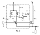
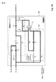
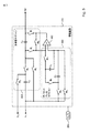
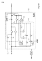
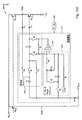
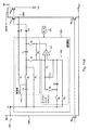
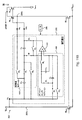
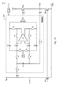
・キャパシタを用いて、モニタリングされているノード(例えば、208a)と制御ノード(例えば、208b)との間の電位差(誤差)を測定すること。
・集積器を使用してキャパシタ上の電荷を第2のキャパシタ上に集積する。
・誤差をゼロにドライブするために負のフィードバックループにおいて集積器を使用すること。
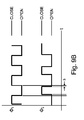
・1つの位相(例えば、Φ2)において、
−オフセットキャパシタ(例えば、C1)上に増幅器のDCオフセットをサンプリングする。
−誤差キャパシタ(例えば、C3)上に誤差をサンプリングする。
−誤差を低減するために出力キャパシタ(例えば、C2)を使用する。
・別の位相(例えば、Φ1)において、
−サンプリングされた誤差を出力キャパシタ上に集積するために増幅器を使用する。
−誤差を低減するために増幅器を使用する。
−DCオフセットを補償するためにオフセットキャパシタを使用する。
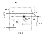
[0056]本開示に係る実施形態は、より正確な電流感知を供給することができる。特定の実施形態では、電流感知における正確性は、感知トランジスタ上への伝送トランジスタの電圧降下のより正確な複製によって達成されることができる。本開示に係る実施形態は、連続したオン動作を提供することができるシングルオペアンプ自動ゼロ化設計を使用して増幅器におけるDCオフセットを低減することができる。
Claims (26)
- 回路であって、
第1の回路入力及び第2の回路入力と、
回路出力と、
第1のキャパシタと、
前記回路出力に接続された第2のキャパシタと、
第1の増幅器入力及び第2の増幅器入力並びに増幅器出力を有する増幅器と、
第1の構成で動作可能であり、第2の構成で動作可能である複数のスイッチと
を備え、
前記スイッチの前記第1の構成では、
前記増幅器出力は、前記回路出力から切断され、
前記第1のキャパシタは、前記増幅器のDCオフセットを感知するために、前記増幅器入力間に接続され、
前記第2のキャパシタは、前記回路出力と前記回路入力のうちの1つとの間にのみ接続され、
前記スイッチの前記第2の構成では、
前記増幅器出力は、前記回路出力に接続され、
前記第1のキャパシタは、前記増幅器の前記DCオフセットを補償するために、前記増幅器入力のうちの1つに接続され、
前記第2のキャパシタは、フィードバックループにおいて前記増幅器に接続される、
回路。 - 第3のキャパシタを更に備え、ここにおいて、前記スイッチの前記第1の構成では、前記第3のキャパシタは、前記回路入力間にのみ接続され、前記スイッチの前記第2の構成では、前記第3のキャパシタは、前記第3のキャパシタの電荷を前記増幅器を使用して前記第2のキャパシタに集積するために、前記第2のキャパシタ及び前記増幅器の両方に接続される、請求項1に記載の回路。
- 前記スイッチの前記第1の構成及び前記スイッチの前記第2の構成の両方において、前記回路入力のうちの1つは、前記第1のキャパシタ、前記第2のキャパシタ及び前記増幅器に共通である電圧基準点を提供するために接続される、請求項1に記載の回路。
- 前記スイッチの前記第1の構成において、前記第1のキャパシタは、前記増幅器入力のうちの1つと前記回路入力のうちの1つとの間に接続される、請求項1に記載の回路。
- 前記第1の回路入力は、第1のトランジスタに接続され、前記第2の回路入力は、第2のトランジスタに接続される、請求項1に記載の回路。
- 前記第1のトランジスタ及び前記第2のトランジスタは、電流ミラー構成で接続される、請求項5に記載の回路。
- 前記回路出力は、第1のトランジスタを備える出力段に接続される、請求項1に記載の回路。
- 前記第1のトランジスタは、カスコードとして第2のトランジスタに接続される、請求項7に記載の回路。
- 前記第1のトランジスタは、電流ミラーとして第2のトランジスタに接続される、請求項7に記載の回路。
- 回路であって、
第1の回路入力及び第2の回路入力と、
回路出力と、
出力を有する増幅器と、ここで、前記出力は、前記回路出力に接続されない第1の構成と、前記回路出力に接続される第2の構成とを有し、
前記回路出力に接続された出力キャパシタと、ここで、前記出力キャパシタは、フィードバックループにおいて前記増幅器に接続された第1の構成と、前記増幅器に接続されない第2の構成とを有し、
前記第1の回路入力に接続された入力キャパシタと、前記入力キャパシタは、前記出力キャパシタを有するフィードバックループにおいて前記増幅器に接続された第1の構成と、前記第2の回路入力にのみ接続された第2の構成とを有する、
前記増幅器の第1の入力及び第2の入力に接続された第1の構成を有し、前記入力キャパシタが前記出力キャパシタを有する前記フィードバックループにおいて前記増幅器に接続されたときに、前記入力キャパシタと直列に接続された第2の構成を有する第1のオフセットキャパシタと
を備える回路。 - 前記増幅器、前記出力キャパシタ、前記入力キャパシタ及び前記オフセットキャパシタに接続された複数のスイッチを更に備え、各スイッチは、開位置及び閉位置へと選択的に動作可能である、請求項10に記載の回路。
- 前記スイッチを動作するための制御信号を受けるために1つ以上の制御入力を更に備える、請求項11に記載の回路。
- 前記増幅器を前記第1の構成に、前記出力キャパシタを前記第1の構成に、前記入力キャパシタを前記第1の構成に、前記オフセットキャパシタを前記第1の構成に構成するように、及び前記増幅器を前記第2の構成に、前記出力キャパシタを前記第2の構成に、前記入力キャパシタを前記第2の構成に、前記オフセットキャパシタを前記第2の構成に構成するように動作可能な複数のスイッチを更に備える、請求項10に記載の回路。
- 前記第1のオフセットキャパシタが前記第1の構成であるときに前記第1のオフセットキャパシタから切断されるように、及び前記第1のオフセットキャパシタが前記第2の構成であるときに前記第1のオフセットキャパシタと並列に接続されるように構成可能である第2のオフセットキャパシタを更に備える、請求項10に記載の回路。
- 前記増幅器が前記第1の構成であるときに、前記出力キャパシタは、前記第1の構成であり、前記入力キャパシタは、前記第1の構成であり、前記オフセットキャパシタは、前記第1の構成である、請求項10に記載の回路。
- 前記増幅器が前記第2の構成にあるときに、前記出力キャパシタは、前記第2の構成であり、前記入力キャパシタは、前記第2の構成であり、前記オフセットキャパシタは、前記第2の構成である、請求項15に記載の回路。
- 前記増幅器は、シングルオペアンプを備える、請求項10に記載の回路。
- 回路であって、
負荷に接続可能な出力端子を有する伝送トランジスタと、
前記伝送トランジスタを通る電流フローをミラーリングするために前記伝送トランジスタに接続された感知トランジスタと、
前記感知トランジスタに接続された出力段と、
前記パストランジスタに接続された第1の回路入力と、前記感知トランジスタに接続された第2の回路入力と、前記出力段に接続された回路出力とを有する増幅器回路と
を備え、前記増幅器回路は、
選択的に、前記回路出力に接続可能又は前記回路出力から切断可能である出力を有する増幅器セクションと、
前記回路出力に接続され、且つ、選択的に、前記増幅器セクションと接続可能又は前記増幅器セクションと切断可能である集積器セクションと、
前記増幅器セクションに接続されたオフセットヌル化セクションと
を備え、
ここにおいて、前記増幅器セクションは、前記オフセットヌル化セクションが前記増幅器のオフセットをサンプリングしているときに、前記回路出力から切断され、
前記集積器セクションは、前記増幅器セクションが前記回路出力から切断されているときに、前記出力段をドライブするために前記回路出力の出力を供給する、
回路。 - 前記集積器セクションは、前記増幅器セクションが前記回路出力から切断されているときに、前記増幅器回路の前記第1の回路入力と前記第2の回路入力との間の電圧差を更に格納する、請求項18に記載の回路。
- 前記増幅器セクションは、前記集積器セクションが、フィードバックループ構成において前記増幅器セクションに接続されているときに、前記出力段をドライブするために前記回路出力に接続される、請求項18に記載の回路。
- 前記オフセットヌル化セクションは、前記集積器セクションが前記増幅器セクションに接続されているときに、サンプリングされたDCオフセットを使用して前記増幅器セクションのDCオフセットを補償する、請求項20に記載の回路。
- 前記出力段は、カスコードとして前記感知トランジスタに接続されたトランジスタを備える、請求項18に記載の回路。
- 前記出力段は、電流ミラーを備える、請求項18に記載の回路。
- 前記伝送トランジスタは、制御源に接続可能な制御入力を更に有する、請求項18に記載の回路。
- 前記制御源は、低ドロップアウトレギュレータの誤差増幅器である、請求項24に記載の回路。
- 回路であって、
第1の回路入力及び第2の回路入力と、
回路出力と、
第1のキャパシタと、
第2のキャパシタと、
第1の増幅器入力及び第2の増幅器入力並びに差動出力を有する差動増幅器と、
前記回路出力に接続された出力増幅器と、ここで、前記第2のキャパシタは、前記出力増幅器に接続され、
第1の構成で動作可能であり、第2の構成で動作可能である複数のスイッチと
を備え、
ここにおいて、前記スイッチの前記第1の構成では、
前記差動出力は、前記出力増幅器から切断され、
前記第1のキャパシタは、前記差動増幅器のDCオフセットを感知するために前記増幅器の入力間に接続される、
前記第2のキャパシタは、前記出力増幅器と前記増幅器入力との間にのみ接続され、
前記スイッチの前記第2の構成では、
前記差動出力は、前記出力増幅器に接続され、
前記第1のキャパシタは、前記増幅器の前記DCオフセットを補償するために、前記増幅器入力に接続され、
前記第2のキャパシタは、フィードバックループにおいて前記差動増幅器に接続される、
回路。
Applications Claiming Priority (3)
| Application Number | Priority Date | Filing Date | Title |
|---|---|---|---|
| US14/329,615 US9444414B2 (en) | 2014-07-11 | 2014-07-11 | Current sense circuit using a single opamp having DC offset auto-zeroing |
| US14/329,615 | 2014-07-11 | ||
| PCT/US2015/038126 WO2016007316A1 (en) | 2014-07-11 | 2015-06-26 | Current sense circuit using a single opamp having dc offset auto-zeroing |
Publications (2)
| Publication Number | Publication Date |
|---|---|
| JP2017526247A true JP2017526247A (ja) | 2017-09-07 |
| JP2017526247A5 JP2017526247A5 (ja) | 2018-07-19 |
Family
ID=53525307
Family Applications (1)
| Application Number | Title | Priority Date | Filing Date |
|---|---|---|---|
| JP2017500914A Pending JP2017526247A (ja) | 2014-07-11 | 2015-06-26 | Dcオフセット自動ゼロ化を有するシングルオペアンプを使用した電流感知回路 |
Country Status (5)
| Country | Link |
|---|---|
| US (1) | US9444414B2 (ja) |
| EP (1) | EP3167546B1 (ja) |
| JP (1) | JP2017526247A (ja) |
| CN (1) | CN106464215B (ja) |
| WO (1) | WO2016007316A1 (ja) |
Cited By (3)
| Publication number | Priority date | Publication date | Assignee | Title |
|---|---|---|---|---|
| JP2019168892A (ja) * | 2018-03-23 | 2019-10-03 | 富士電機株式会社 | 演算増幅回路及びこれを使用した電流検出装置 |
| JP2019185786A (ja) * | 2018-04-12 | 2019-10-24 | アナログ・ディヴァイシス・グローバル・アンリミテッド・カンパニー | 高駆動能力を有する低電力ハーフvdd生成回路 |
| JP2023121617A (ja) * | 2022-02-21 | 2023-08-31 | 富士電機株式会社 | 半導体装置 |
Families Citing this family (20)
| Publication number | Priority date | Publication date | Assignee | Title |
|---|---|---|---|---|
| US10038408B2 (en) * | 2015-06-26 | 2018-07-31 | Cactus Semiconductor, Inc. | Pseudo-random chopper amplifier |
| US9973183B2 (en) * | 2015-09-28 | 2018-05-15 | Power Integrations, Inc. | Field-effect transistor device with partial finger current sensing FETs |
| US9983239B2 (en) | 2016-05-13 | 2018-05-29 | Power Integrations, Inc. | Integrated linear current sense circuitry for semiconductor transistor devices |
| TWI638145B (zh) * | 2016-06-27 | 2018-10-11 | 友達光電股份有限公司 | 感測電路及感測電路的控制方法 |
| JP6953512B2 (ja) | 2016-08-08 | 2021-10-27 | パワー・インテグレーションズ・インコーポレーテッド | 半導体スイッチングデバイスの高速温度検出のための集積回路 |
| IT201700058135A1 (it) * | 2017-05-29 | 2018-11-29 | St Microelectronics Srl | Circuito di rilevazione, dispositivo e procedimento corrispondenti |
| EP3537336B1 (en) * | 2017-11-07 | 2021-03-17 | Shenzhen Goodix Technology Co., Ltd. | Fingerprint sensor and terminal device |
| JP6937705B2 (ja) * | 2018-01-30 | 2021-09-22 | ルネサスエレクトロニクス株式会社 | 半導体装置、電流検出方法および負荷駆動システム |
| US11047946B2 (en) * | 2018-05-08 | 2021-06-29 | Qualcomm Incorporated | Differential current sensing with robust path, voltage offset removal and process, voltage, temperature (PVT) tolerance |
| WO2020010125A1 (en) * | 2018-07-04 | 2020-01-09 | Texas Instruments Incorporated | Current sense circuit stabilized over wide range of load current |
| US10784829B2 (en) | 2018-07-04 | 2020-09-22 | Texas Instruments Incorporated | Current sense circuit stabilized over wide range of load current |
| US11012037B2 (en) | 2019-03-22 | 2021-05-18 | Analog Devices International Unlimited Company | Techniques for controlling an auto-zero amplifier |
| JP7161432B2 (ja) * | 2019-03-25 | 2022-10-26 | ルネサスエレクトロニクス株式会社 | 電流検出回路、半導体装置、及び、半導体システム |
| US10833639B2 (en) | 2019-04-12 | 2020-11-10 | Analog Devices International Unlimited Company | Method for aliasing reduction in auto zero amplifier |
| EP3951551B1 (en) * | 2020-08-07 | 2023-02-22 | Scalinx | Voltage regulator and method |
| US11422168B2 (en) | 2020-09-16 | 2022-08-23 | Nxp Usa, Inc. | On-chip, low-voltage, current sensing circuit |
| US11499995B2 (en) | 2020-10-26 | 2022-11-15 | Analog Devices, Inc. | Leakage compensation technique for current sensor |
| US11923815B2 (en) | 2021-06-06 | 2024-03-05 | Trieye Ltd. | Electronic integration circuit having offset and collected charge reduction circuitries and associated methods |
| US12321185B2 (en) | 2022-01-07 | 2025-06-03 | Samsung Electronics Co., Ltd. | Low dropout regulator providing variable offset and analog to digital conversion circuit including the same |
| US12607658B2 (en) | 2023-03-21 | 2026-04-21 | Qualcomm Incorporated | Current sensor with a time-interleaved impedance compensation scheme |
Citations (8)
| Publication number | Priority date | Publication date | Assignee | Title |
|---|---|---|---|---|
| JP2004222018A (ja) * | 2003-01-16 | 2004-08-05 | Seiko Instruments Inc | スイッチトキャパシタ増幅回路 |
| JP2005020291A (ja) * | 2003-06-25 | 2005-01-20 | Toyota Motor Corp | オフセットキャンセル型オペアンプ回路 |
| JP2005100296A (ja) * | 2003-08-29 | 2005-04-14 | Ricoh Co Ltd | 定電圧回路 |
| JP2007208924A (ja) * | 2006-02-06 | 2007-08-16 | Seiko Instruments Inc | スイッチドキャパシタアンプ及びスイッチドキャパシタアンプの動作方法 |
| JP2008067050A (ja) * | 2006-09-07 | 2008-03-21 | Handotai Rikougaku Kenkyu Center:Kk | 帰還型増幅回路 |
| US20080116966A1 (en) * | 2006-11-21 | 2008-05-22 | Youngcheol Chae | Switched capacitor circuit with inverting amplifier and offset unit |
| US20100079204A1 (en) * | 2008-09-29 | 2010-04-01 | Detlef Ummelmann | Switched-capacitor amplifier arrangement having a low input current |
| JP2012044347A (ja) * | 2010-08-17 | 2012-03-01 | Seiko Epson Corp | 集積回路装置及び電子機器 |
Family Cites Families (7)
| Publication number | Priority date | Publication date | Assignee | Title |
|---|---|---|---|---|
| US5479130A (en) * | 1994-02-15 | 1995-12-26 | Analog Devices, Inc. | Auto-zero switched-capacitor integrator |
| US6781450B1 (en) * | 2003-03-07 | 2004-08-24 | National Semiconductor Corporation | Low-frequency auto-zeroed amplifier |
| US7321260B2 (en) | 2006-03-07 | 2008-01-22 | Honeywell International, Inc. | Ping-pong auto-zero amplifier with glitch reduction |
| US20090273392A1 (en) | 2008-05-01 | 2009-11-05 | Custom One Design, Inc. | Methods and apparatus for reducing non-ideal effects in correlated double sampling compensated circuits |
| US8743630B2 (en) * | 2011-05-23 | 2014-06-03 | Infineon Technologies Ag | Current sense amplifier with replica bias scheme |
| US8624766B2 (en) | 2011-11-30 | 2014-01-07 | Standard Microsystems Corporation | Method and system for auto-ranging analog-to-digital converter for current sensing |
| TW201506873A (zh) * | 2013-08-02 | 2015-02-16 | Integrated Solutions Technology Inc | 有機發光顯示器的驅動電路以及偏移電壓調整單元 |
-
2014
- 2014-07-11 US US14/329,615 patent/US9444414B2/en active Active
-
2015
- 2015-06-26 JP JP2017500914A patent/JP2017526247A/ja active Pending
- 2015-06-26 WO PCT/US2015/038126 patent/WO2016007316A1/en not_active Ceased
- 2015-06-26 CN CN201580033648.1A patent/CN106464215B/zh active Active
- 2015-06-26 EP EP15735829.2A patent/EP3167546B1/en active Active
Patent Citations (8)
| Publication number | Priority date | Publication date | Assignee | Title |
|---|---|---|---|---|
| JP2004222018A (ja) * | 2003-01-16 | 2004-08-05 | Seiko Instruments Inc | スイッチトキャパシタ増幅回路 |
| JP2005020291A (ja) * | 2003-06-25 | 2005-01-20 | Toyota Motor Corp | オフセットキャンセル型オペアンプ回路 |
| JP2005100296A (ja) * | 2003-08-29 | 2005-04-14 | Ricoh Co Ltd | 定電圧回路 |
| JP2007208924A (ja) * | 2006-02-06 | 2007-08-16 | Seiko Instruments Inc | スイッチドキャパシタアンプ及びスイッチドキャパシタアンプの動作方法 |
| JP2008067050A (ja) * | 2006-09-07 | 2008-03-21 | Handotai Rikougaku Kenkyu Center:Kk | 帰還型増幅回路 |
| US20080116966A1 (en) * | 2006-11-21 | 2008-05-22 | Youngcheol Chae | Switched capacitor circuit with inverting amplifier and offset unit |
| US20100079204A1 (en) * | 2008-09-29 | 2010-04-01 | Detlef Ummelmann | Switched-capacitor amplifier arrangement having a low input current |
| JP2012044347A (ja) * | 2010-08-17 | 2012-03-01 | Seiko Epson Corp | 集積回路装置及び電子機器 |
Cited By (4)
| Publication number | Priority date | Publication date | Assignee | Title |
|---|---|---|---|---|
| JP2019168892A (ja) * | 2018-03-23 | 2019-10-03 | 富士電機株式会社 | 演算増幅回路及びこれを使用した電流検出装置 |
| JP7106916B2 (ja) | 2018-03-23 | 2022-07-27 | 富士電機株式会社 | 演算増幅回路及びこれを使用した電流検出装置 |
| JP2019185786A (ja) * | 2018-04-12 | 2019-10-24 | アナログ・ディヴァイシス・グローバル・アンリミテッド・カンパニー | 高駆動能力を有する低電力ハーフvdd生成回路 |
| JP2023121617A (ja) * | 2022-02-21 | 2023-08-31 | 富士電機株式会社 | 半導体装置 |
Also Published As
| Publication number | Publication date |
|---|---|
| EP3167546A1 (en) | 2017-05-17 |
| US20160013765A1 (en) | 2016-01-14 |
| CN106464215A (zh) | 2017-02-22 |
| US9444414B2 (en) | 2016-09-13 |
| WO2016007316A1 (en) | 2016-01-14 |
| CN106464215B (zh) | 2019-11-08 |
| EP3167546B1 (en) | 2018-08-29 |
Similar Documents
| Publication | Publication Date | Title |
|---|---|---|
| US9444414B2 (en) | Current sense circuit using a single opamp having DC offset auto-zeroing | |
| US9166541B2 (en) | Signal processing circuit, resolver digital converter, and multipath nested mirror amplifier | |
| US10234487B2 (en) | Accurate current sensing | |
| US8854125B2 (en) | Linear amplifier that perform level shift and method of level shifting | |
| CN106292824B (zh) | 低压差稳压器电路 | |
| US9128127B2 (en) | Sensor device | |
| US10473698B2 (en) | Voltage monitor | |
| EP1435693B1 (en) | Amplification circuit | |
| JP6602766B2 (ja) | バッテリ用電流感知回路内の増幅器のための補償技術 | |
| CN101043208B (zh) | 放大电路及其增益控制方法 | |
| EP2933910A1 (en) | A multiple output offset comparator | |
| US9755588B2 (en) | Signal output circuit | |
| US8810311B2 (en) | Auto-zeroed amplifier with low input leakage | |
| US20230018651A1 (en) | Regulator circuit and control circuit of dc/dc converter | |
| US9369098B2 (en) | Inverting amplifier | |
| US20250038711A1 (en) | Multi-stage amplifier circuits | |
| US7956690B2 (en) | Operational amplification circuit | |
| JP5616781B2 (ja) | スイッチトキャパシタ型積分器 | |
| EP2779445A1 (en) | Three Stage Amplifier | |
| US8416021B2 (en) | Amplifier circuit | |
| US9768758B2 (en) | Comparison circuit | |
| US20130069728A1 (en) | Automatic bias operational amplifying circuit and system | |
| JP5239875B2 (ja) | バイアス電流生成回路、増幅器及び通信送受信回路 | |
| JP5876807B2 (ja) | 低ドロップアウト電圧レギュレータ回路 | |
| JP2010063072A (ja) | 電圧電流変換回路 |
Legal Events
| Date | Code | Title | Description |
|---|---|---|---|
| A521 | Request for written amendment filed |
Free format text: JAPANESE INTERMEDIATE CODE: A523 Effective date: 20180606 |
|
| A621 | Written request for application examination |
Free format text: JAPANESE INTERMEDIATE CODE: A621 Effective date: 20180606 |
|
| A977 | Report on retrieval |
Free format text: JAPANESE INTERMEDIATE CODE: A971007 Effective date: 20190329 |
|
| A131 | Notification of reasons for refusal |
Free format text: JAPANESE INTERMEDIATE CODE: A131 Effective date: 20190507 |
|
| A02 | Decision of refusal |
Free format text: JAPANESE INTERMEDIATE CODE: A02 Effective date: 20191203 |