JP2017534083A - 軟質電気光学セルを生成する方法 - Google Patents
軟質電気光学セルを生成する方法 Download PDFInfo
- Publication number
- JP2017534083A JP2017534083A JP2017526079A JP2017526079A JP2017534083A JP 2017534083 A JP2017534083 A JP 2017534083A JP 2017526079 A JP2017526079 A JP 2017526079A JP 2017526079 A JP2017526079 A JP 2017526079A JP 2017534083 A JP2017534083 A JP 2017534083A
- Authority
- JP
- Japan
- Prior art keywords
- substrate
- electro
- boundary
- optic material
- liquid crystal
- Prior art date
- Legal status (The legal status is an assumption and is not a legal conclusion. Google has not performed a legal analysis and makes no representation as to the accuracy of the status listed.)
- Granted
Links
Images






Classifications
-
- G—PHYSICS
- G02—OPTICS
- G02F—OPTICAL DEVICES OR ARRANGEMENTS FOR THE CONTROL OF LIGHT BY MODIFICATION OF THE OPTICAL PROPERTIES OF THE MEDIA OF THE ELEMENTS INVOLVED THEREIN; NON-LINEAR OPTICS; FREQUENCY-CHANGING OF LIGHT; OPTICAL LOGIC ELEMENTS; OPTICAL ANALOGUE/DIGITAL CONVERTERS
- G02F1/00—Devices or arrangements for the control of the intensity, colour, phase, polarisation or direction of light arriving from an independent light source, e.g. switching, gating or modulating; Non-linear optics
- G02F1/01—Devices or arrangements for the control of the intensity, colour, phase, polarisation or direction of light arriving from an independent light source, e.g. switching, gating or modulating; Non-linear optics for the control of the intensity, phase, polarisation or colour
- G02F1/13—Devices or arrangements for the control of the intensity, colour, phase, polarisation or direction of light arriving from an independent light source, e.g. switching, gating or modulating; Non-linear optics for the control of the intensity, phase, polarisation or colour based on liquid crystals, e.g. single liquid crystal display cells
- G02F1/133—Constructional arrangements; Operation of liquid crystal cells; Circuit arrangements
- G02F1/1333—Constructional arrangements; Manufacturing methods
- G02F1/1341—Filling or closing of cells
-
- G—PHYSICS
- G02—OPTICS
- G02F—OPTICAL DEVICES OR ARRANGEMENTS FOR THE CONTROL OF LIGHT BY MODIFICATION OF THE OPTICAL PROPERTIES OF THE MEDIA OF THE ELEMENTS INVOLVED THEREIN; NON-LINEAR OPTICS; FREQUENCY-CHANGING OF LIGHT; OPTICAL LOGIC ELEMENTS; OPTICAL ANALOGUE/DIGITAL CONVERTERS
- G02F1/00—Devices or arrangements for the control of the intensity, colour, phase, polarisation or direction of light arriving from an independent light source, e.g. switching, gating or modulating; Non-linear optics
- G02F1/01—Devices or arrangements for the control of the intensity, colour, phase, polarisation or direction of light arriving from an independent light source, e.g. switching, gating or modulating; Non-linear optics for the control of the intensity, phase, polarisation or colour
- G02F1/13—Devices or arrangements for the control of the intensity, colour, phase, polarisation or direction of light arriving from an independent light source, e.g. switching, gating or modulating; Non-linear optics for the control of the intensity, phase, polarisation or colour based on liquid crystals, e.g. single liquid crystal display cells
- G02F1/1303—Apparatus specially adapted to the manufacture of LCDs
-
- G—PHYSICS
- G02—OPTICS
- G02F—OPTICAL DEVICES OR ARRANGEMENTS FOR THE CONTROL OF LIGHT BY MODIFICATION OF THE OPTICAL PROPERTIES OF THE MEDIA OF THE ELEMENTS INVOLVED THEREIN; NON-LINEAR OPTICS; FREQUENCY-CHANGING OF LIGHT; OPTICAL LOGIC ELEMENTS; OPTICAL ANALOGUE/DIGITAL CONVERTERS
- G02F1/00—Devices or arrangements for the control of the intensity, colour, phase, polarisation or direction of light arriving from an independent light source, e.g. switching, gating or modulating; Non-linear optics
- G02F1/01—Devices or arrangements for the control of the intensity, colour, phase, polarisation or direction of light arriving from an independent light source, e.g. switching, gating or modulating; Non-linear optics for the control of the intensity, phase, polarisation or colour
- G02F1/13—Devices or arrangements for the control of the intensity, colour, phase, polarisation or direction of light arriving from an independent light source, e.g. switching, gating or modulating; Non-linear optics for the control of the intensity, phase, polarisation or colour based on liquid crystals, e.g. single liquid crystal display cells
- G02F1/133—Constructional arrangements; Operation of liquid crystal cells; Circuit arrangements
- G02F1/1333—Constructional arrangements; Manufacturing methods
- G02F1/133305—Flexible substrates, e.g. plastics, organic film
-
- G—PHYSICS
- G02—OPTICS
- G02F—OPTICAL DEVICES OR ARRANGEMENTS FOR THE CONTROL OF LIGHT BY MODIFICATION OF THE OPTICAL PROPERTIES OF THE MEDIA OF THE ELEMENTS INVOLVED THEREIN; NON-LINEAR OPTICS; FREQUENCY-CHANGING OF LIGHT; OPTICAL LOGIC ELEMENTS; OPTICAL ANALOGUE/DIGITAL CONVERTERS
- G02F1/00—Devices or arrangements for the control of the intensity, colour, phase, polarisation or direction of light arriving from an independent light source, e.g. switching, gating or modulating; Non-linear optics
- G02F1/01—Devices or arrangements for the control of the intensity, colour, phase, polarisation or direction of light arriving from an independent light source, e.g. switching, gating or modulating; Non-linear optics for the control of the intensity, phase, polarisation or colour
- G02F1/13—Devices or arrangements for the control of the intensity, colour, phase, polarisation or direction of light arriving from an independent light source, e.g. switching, gating or modulating; Non-linear optics for the control of the intensity, phase, polarisation or colour based on liquid crystals, e.g. single liquid crystal display cells
- G02F1/133—Constructional arrangements; Operation of liquid crystal cells; Circuit arrangements
- G02F1/1333—Constructional arrangements; Manufacturing methods
- G02F1/133351—Manufacturing of individual cells out of a plurality of cells, e.g. by dicing
-
- G—PHYSICS
- G02—OPTICS
- G02F—OPTICAL DEVICES OR ARRANGEMENTS FOR THE CONTROL OF LIGHT BY MODIFICATION OF THE OPTICAL PROPERTIES OF THE MEDIA OF THE ELEMENTS INVOLVED THEREIN; NON-LINEAR OPTICS; FREQUENCY-CHANGING OF LIGHT; OPTICAL LOGIC ELEMENTS; OPTICAL ANALOGUE/DIGITAL CONVERTERS
- G02F1/00—Devices or arrangements for the control of the intensity, colour, phase, polarisation or direction of light arriving from an independent light source, e.g. switching, gating or modulating; Non-linear optics
- G02F1/01—Devices or arrangements for the control of the intensity, colour, phase, polarisation or direction of light arriving from an independent light source, e.g. switching, gating or modulating; Non-linear optics for the control of the intensity, phase, polarisation or colour
- G02F1/13—Devices or arrangements for the control of the intensity, colour, phase, polarisation or direction of light arriving from an independent light source, e.g. switching, gating or modulating; Non-linear optics for the control of the intensity, phase, polarisation or colour based on liquid crystals, e.g. single liquid crystal display cells
- G02F1/133—Constructional arrangements; Operation of liquid crystal cells; Circuit arrangements
- G02F1/1333—Constructional arrangements; Manufacturing methods
- G02F1/133377—Cells with plural compartments or having plurality of liquid crystal microcells partitioned by walls, e.g. one microcell per pixel
-
- G—PHYSICS
- G02—OPTICS
- G02F—OPTICAL DEVICES OR ARRANGEMENTS FOR THE CONTROL OF LIGHT BY MODIFICATION OF THE OPTICAL PROPERTIES OF THE MEDIA OF THE ELEMENTS INVOLVED THEREIN; NON-LINEAR OPTICS; FREQUENCY-CHANGING OF LIGHT; OPTICAL LOGIC ELEMENTS; OPTICAL ANALOGUE/DIGITAL CONVERTERS
- G02F1/00—Devices or arrangements for the control of the intensity, colour, phase, polarisation or direction of light arriving from an independent light source, e.g. switching, gating or modulating; Non-linear optics
- G02F1/01—Devices or arrangements for the control of the intensity, colour, phase, polarisation or direction of light arriving from an independent light source, e.g. switching, gating or modulating; Non-linear optics for the control of the intensity, phase, polarisation or colour
- G02F1/13—Devices or arrangements for the control of the intensity, colour, phase, polarisation or direction of light arriving from an independent light source, e.g. switching, gating or modulating; Non-linear optics for the control of the intensity, phase, polarisation or colour based on liquid crystals, e.g. single liquid crystal display cells
- G02F1/133—Constructional arrangements; Operation of liquid crystal cells; Circuit arrangements
- G02F1/1333—Constructional arrangements; Manufacturing methods
- G02F1/1337—Surface-induced orientation of the liquid crystal molecules, e.g. by alignment layers
-
- G—PHYSICS
- G02—OPTICS
- G02F—OPTICAL DEVICES OR ARRANGEMENTS FOR THE CONTROL OF LIGHT BY MODIFICATION OF THE OPTICAL PROPERTIES OF THE MEDIA OF THE ELEMENTS INVOLVED THEREIN; NON-LINEAR OPTICS; FREQUENCY-CHANGING OF LIGHT; OPTICAL LOGIC ELEMENTS; OPTICAL ANALOGUE/DIGITAL CONVERTERS
- G02F1/00—Devices or arrangements for the control of the intensity, colour, phase, polarisation or direction of light arriving from an independent light source, e.g. switching, gating or modulating; Non-linear optics
- G02F1/01—Devices or arrangements for the control of the intensity, colour, phase, polarisation or direction of light arriving from an independent light source, e.g. switching, gating or modulating; Non-linear optics for the control of the intensity, phase, polarisation or colour
- G02F1/13—Devices or arrangements for the control of the intensity, colour, phase, polarisation or direction of light arriving from an independent light source, e.g. switching, gating or modulating; Non-linear optics for the control of the intensity, phase, polarisation or colour based on liquid crystals, e.g. single liquid crystal display cells
- G02F1/133—Constructional arrangements; Operation of liquid crystal cells; Circuit arrangements
- G02F1/1333—Constructional arrangements; Manufacturing methods
- G02F1/1339—Gaskets; Spacers; Sealing of cells
-
- G—PHYSICS
- G02—OPTICS
- G02F—OPTICAL DEVICES OR ARRANGEMENTS FOR THE CONTROL OF LIGHT BY MODIFICATION OF THE OPTICAL PROPERTIES OF THE MEDIA OF THE ELEMENTS INVOLVED THEREIN; NON-LINEAR OPTICS; FREQUENCY-CHANGING OF LIGHT; OPTICAL LOGIC ELEMENTS; OPTICAL ANALOGUE/DIGITAL CONVERTERS
- G02F1/00—Devices or arrangements for the control of the intensity, colour, phase, polarisation or direction of light arriving from an independent light source, e.g. switching, gating or modulating; Non-linear optics
- G02F1/01—Devices or arrangements for the control of the intensity, colour, phase, polarisation or direction of light arriving from an independent light source, e.g. switching, gating or modulating; Non-linear optics for the control of the intensity, phase, polarisation or colour
- G02F1/13—Devices or arrangements for the control of the intensity, colour, phase, polarisation or direction of light arriving from an independent light source, e.g. switching, gating or modulating; Non-linear optics for the control of the intensity, phase, polarisation or colour based on liquid crystals, e.g. single liquid crystal display cells
- G02F1/133—Constructional arrangements; Operation of liquid crystal cells; Circuit arrangements
- G02F1/1333—Constructional arrangements; Manufacturing methods
- G02F1/1339—Gaskets; Spacers; Sealing of cells
- G02F1/13392—Gaskets; Spacers; Sealing of cells spacers dispersed on the cell substrate, e.g. spherical particles, microfibres
-
- G—PHYSICS
- G02—OPTICS
- G02F—OPTICAL DEVICES OR ARRANGEMENTS FOR THE CONTROL OF LIGHT BY MODIFICATION OF THE OPTICAL PROPERTIES OF THE MEDIA OF THE ELEMENTS INVOLVED THEREIN; NON-LINEAR OPTICS; FREQUENCY-CHANGING OF LIGHT; OPTICAL LOGIC ELEMENTS; OPTICAL ANALOGUE/DIGITAL CONVERTERS
- G02F1/00—Devices or arrangements for the control of the intensity, colour, phase, polarisation or direction of light arriving from an independent light source, e.g. switching, gating or modulating; Non-linear optics
- G02F1/01—Devices or arrangements for the control of the intensity, colour, phase, polarisation or direction of light arriving from an independent light source, e.g. switching, gating or modulating; Non-linear optics for the control of the intensity, phase, polarisation or colour
- G02F1/13—Devices or arrangements for the control of the intensity, colour, phase, polarisation or direction of light arriving from an independent light source, e.g. switching, gating or modulating; Non-linear optics for the control of the intensity, phase, polarisation or colour based on liquid crystals, e.g. single liquid crystal display cells
- G02F1/133—Constructional arrangements; Operation of liquid crystal cells; Circuit arrangements
- G02F1/1333—Constructional arrangements; Manufacturing methods
- G02F1/1339—Gaskets; Spacers; Sealing of cells
- G02F1/13394—Gaskets; Spacers; Sealing of cells spacers regularly patterned on the cell subtrate, e.g. walls, pillars
-
- G—PHYSICS
- G02—OPTICS
- G02F—OPTICAL DEVICES OR ARRANGEMENTS FOR THE CONTROL OF LIGHT BY MODIFICATION OF THE OPTICAL PROPERTIES OF THE MEDIA OF THE ELEMENTS INVOLVED THEREIN; NON-LINEAR OPTICS; FREQUENCY-CHANGING OF LIGHT; OPTICAL LOGIC ELEMENTS; OPTICAL ANALOGUE/DIGITAL CONVERTERS
- G02F1/00—Devices or arrangements for the control of the intensity, colour, phase, polarisation or direction of light arriving from an independent light source, e.g. switching, gating or modulating; Non-linear optics
- G02F1/01—Devices or arrangements for the control of the intensity, colour, phase, polarisation or direction of light arriving from an independent light source, e.g. switching, gating or modulating; Non-linear optics for the control of the intensity, phase, polarisation or colour
- G02F1/13—Devices or arrangements for the control of the intensity, colour, phase, polarisation or direction of light arriving from an independent light source, e.g. switching, gating or modulating; Non-linear optics for the control of the intensity, phase, polarisation or colour based on liquid crystals, e.g. single liquid crystal display cells
- G02F1/133—Constructional arrangements; Operation of liquid crystal cells; Circuit arrangements
- G02F1/1333—Constructional arrangements; Manufacturing methods
- G02F1/1343—Electrodes
- G02F1/13439—Electrodes characterised by their electrical, optical, physical properties; materials therefor; method of making
-
- G—PHYSICS
- G02—OPTICS
- G02F—OPTICAL DEVICES OR ARRANGEMENTS FOR THE CONTROL OF LIGHT BY MODIFICATION OF THE OPTICAL PROPERTIES OF THE MEDIA OF THE ELEMENTS INVOLVED THEREIN; NON-LINEAR OPTICS; FREQUENCY-CHANGING OF LIGHT; OPTICAL LOGIC ELEMENTS; OPTICAL ANALOGUE/DIGITAL CONVERTERS
- G02F1/00—Devices or arrangements for the control of the intensity, colour, phase, polarisation or direction of light arriving from an independent light source, e.g. switching, gating or modulating; Non-linear optics
- G02F1/01—Devices or arrangements for the control of the intensity, colour, phase, polarisation or direction of light arriving from an independent light source, e.g. switching, gating or modulating; Non-linear optics for the control of the intensity, phase, polarisation or colour
- G02F1/13—Devices or arrangements for the control of the intensity, colour, phase, polarisation or direction of light arriving from an independent light source, e.g. switching, gating or modulating; Non-linear optics for the control of the intensity, phase, polarisation or colour based on liquid crystals, e.g. single liquid crystal display cells
- G02F1/133—Constructional arrangements; Operation of liquid crystal cells; Circuit arrangements
- G02F1/1333—Constructional arrangements; Manufacturing methods
- G02F1/133354—Arrangements for aligning or assembling substrates
-
- G—PHYSICS
- G02—OPTICS
- G02F—OPTICAL DEVICES OR ARRANGEMENTS FOR THE CONTROL OF LIGHT BY MODIFICATION OF THE OPTICAL PROPERTIES OF THE MEDIA OF THE ELEMENTS INVOLVED THEREIN; NON-LINEAR OPTICS; FREQUENCY-CHANGING OF LIGHT; OPTICAL LOGIC ELEMENTS; OPTICAL ANALOGUE/DIGITAL CONVERTERS
- G02F1/00—Devices or arrangements for the control of the intensity, colour, phase, polarisation or direction of light arriving from an independent light source, e.g. switching, gating or modulating; Non-linear optics
- G02F1/01—Devices or arrangements for the control of the intensity, colour, phase, polarisation or direction of light arriving from an independent light source, e.g. switching, gating or modulating; Non-linear optics for the control of the intensity, phase, polarisation or colour
- G02F1/13—Devices or arrangements for the control of the intensity, colour, phase, polarisation or direction of light arriving from an independent light source, e.g. switching, gating or modulating; Non-linear optics for the control of the intensity, phase, polarisation or colour based on liquid crystals, e.g. single liquid crystal display cells
- G02F1/133—Constructional arrangements; Operation of liquid crystal cells; Circuit arrangements
- G02F1/1333—Constructional arrangements; Manufacturing methods
- G02F1/1339—Gaskets; Spacers; Sealing of cells
- G02F1/13398—Spacer materials; Spacer properties
Landscapes
- Physics & Mathematics (AREA)
- Nonlinear Science (AREA)
- Chemical & Material Sciences (AREA)
- Crystallography & Structural Chemistry (AREA)
- General Physics & Mathematics (AREA)
- Optics & Photonics (AREA)
- Mathematical Physics (AREA)
- Engineering & Computer Science (AREA)
- Manufacturing & Machinery (AREA)
- Liquid Crystal (AREA)
- Spectroscopy & Molecular Physics (AREA)
- Electrochromic Elements, Electrophoresis, Or Variable Reflection Or Absorption Elements (AREA)
Abstract
Description
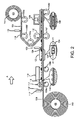
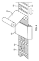
図4に示す製造方法の別の実施形態では、いかなる境界シールもロールフィル工程の前に塗布されない。むしろ、一定量のEOM270が基板272上へ塗布され、次に、要望により予め被覆された2つの基板272、274が一緒にされEOMでロールフィルされ、それらの分離性は一方または両方の基板上でスペーサにより維持される。ロールフィルの工程は単一または二重ローラにより行われ得る。
●ITOとアライメント層PIにより予め被覆された2つの基板が、一方が上部基板を形成し他方は下部基板を形成する一組のローラ上に配置される、
●下部基板は非パターン化スペーサで噴霧される、
●境界封止剤が下部基板上へ印刷される、
●液晶/染料混合物の線が境界封止剤の周囲外に蒸着される、
●ローラは、上部および下部基板を一緒にし、境界封止剤の周囲の内部の活性領域を液晶/染料混合物でロールフィルするために使用される、
●境界封止剤はエッジシールを形成するためにUV硬化される。
図6に示す別の実施例では、下部基板は、セル120をロールフィルするために使用される移動プレート150および単一ローラ(110’)上に配置され、それへ固定され得る。この実施例では、移動ローラ110’がプレートおよび/または下部基板の方向Aの運動を引き起こし得るか、または移動プレート150が下部基板を移動し、ローラを方向Bに転回させ、基板同士を対にし、セルをロールフィルするかのいずれかである。
この実施例では(図7)、一組の上部および下部ローラ200、202が、上部軟質基板204を下部軟質基板206へ嵌合するまたはこれらを対にするために使用される。境界封止剤208が下部基板206へ塗布される。ローラ200、202はローラ自身を介し軟質基板をウェブ方向Aに引っ張る。転回中、蒸着された電気光学混合物210は、2つの基板204、206が対にされている間に、2つの基板204、206間に生成された制御ギャップを同時に満たす。
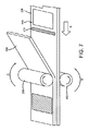
この実施例では、一組の左右ローラ250、252が、基板を垂直下方向に移動させながら軟質基板254と軟質基板256とを対にするために使用される(図8)。
別の実施例では、基板の2つのロールがそれぞれローラ上に配置される。各ロールは三菱プラスチック社の0.076mm(3mil)PETである。基板ロールはMaterion社による導電層(ITO)で予め被覆される。次に、ITO被覆基板はポリイミドアライメント層(Nissan Chemicals社の5661)で被覆される。直径6マイクロメートルのShinshikyuEWプラスチック球(Hiko Industrial社、香港)が被覆処理中にポリイミド内に混合され、基板ロールの少なくとも一方内に存在する。ローラはロールツーロールプロセス中に基板のロールを巻き戻す。1つの巻き戻されたロールが上部基板になり、第2番目は下部基板になる。基板はロールツーロールプロセス中約1.27cm(0.5インチ)/秒から約2.54cm(10インチ)/秒のウェブ速度で移動する。各基板は当該境界封止剤印刷機を有する。この場合、これらの印刷機は回転スクリーン印刷機である。回転スクリーン印刷機は境界封止剤(Loctite3108)を上部および下部基板の活性面のそれぞれの上に印刷する。活性面は完成セル内のEOMに接することになる面である。回転印刷機は境界封止剤を約5マイクロメートル〜約100マイクロメートル(好適には約5マイクロメートル〜約40マイクロメートル)の高さで印刷するだろう。回転印刷後、EOMは注射器および針分注器により下部基板の活性面上に蒸着される。EOMはゲスト−ホスト二色性染料−液晶混合物(AMI577)である。一組の上部および下部積層化ローラは、上部境界封止剤が下部境界封止剤とアライメントされ、EOMが上部および下部活性面の両方と接触しロールフィルプロセス中に全内部境界封止剤領域を満たすように、上部および下部基板同士を嵌合する。積層化ローラは、積層化中に基板両端に定圧を印加する加圧ローラとなるように構成される、または、上部積層化ローラが下部積層化ローラからある設定距離で離間され、上部および下部基板の間の制御ギャップおよびスペーサを加圧することなく上部および下部基板を嵌合できるようにするギャップ設定ローラとなるように構成される。嵌合された基板は、紫外線、熱、またはUVおよび熱硬化の組み合わせにより、積層化後に硬化される。次に、硬化基板は、追加処理のためにロールから切断されシートにされる。
Claims (20)
- 境界シールにより取り囲まれ電気光学材料により満たされる軟質セルユニットであってスペーサにより維持された制御距離だけ分離された第1の基板と第2の基板を有する軟質セルユニットを生成する方法において、前記方法は、
前記第1の基板と前記第2の基板を形成するために軟質プラスチック材料の2つの連続シートを設ける工程と、
非カプセル化・非重合体状態であり1%未満の重合可能材料を含む電気光学材料を少なくとも一方の基板上に蒸着する工程と、
前記電気光学材料が前記第1の基板と前記第2の基板の間の前記制御距離を完全に満たすように、1つまたは複数の積層化ローラを使用することにより前記軟質セルを前記電気光学材料でロールフィルしながら前記第1の基板と前記第2の基板を対にする工程と、を含む方法。 - 前記ロールフィル工程前に前記第1の基板または前記第2の基板またはその両方上に境界封止剤を塗布し、前記ロールフィル工程後に前記境界シールを形成するために前記境界封止剤を硬化する工程をさらに含む請求項1に記載の方法。
- 前記電気光学材料は前記境界封止剤の周囲外の領域、前記境界封止剤の周囲内の領域、または前記境界封止剤の周囲内および周囲外両方の1つまたは複数の領域上に蒸着される、請求項2に記載の方法。
- 前記ロールフィル工程中、前記電気光学材料の粘度に対する境界封止剤粘度の比は10を越える、請求項2に記載の方法。
- 前記第1、前記第2、または両方の基板上に複数の境界封止剤を塗布する工程を含む、請求項2に記載の方法。
- 機械的ダイ切断機、レーザ切断機、またはそれらの組み合せを使用することにより前記軟質プラスチック材料の2つの連続シートから前記軟質セルユニットを切断する工程をさらに含む請求項2乃至5のいずれか一項に記載の方法。
- 前記ロールフィル工程後に、境界シールを形成し、前記軟質プラスチックの2つの連続シートから前記軟質セルユニットを分離するための形状を切断する工程をさらに含む請求項1に記載の方法。
- 前記第1の基板上に、前記第2の基板上に、前記電気光学材料内に、またはこれらの組み合せに、前記スペーサを蒸着する工程をさらに含む請求項1乃至7のいずれか一項に記載の方法。
- スペーサは非パターン化状態である、請求項1乃至8のいずれか一項に記載の方法。
- 前記第1の基板、前記第2の基板、または両方上にアライメント層を塗布する工程をさらに含む請求項1乃至9のいずれか一項に記載の方法。
- 前記アライメント層内に非パターン化スペーサを蒸着する工程をさらに含む請求項9に記載の方法。
- 一方または両方の基板へ隔壁を追加する工程をさらに含む請求項1乃至11のいずれか一項に記載の方法。
- 前記アライメント層は前記第1の基板と前記第2の基板の一方または両方の基板の選択された活性領域上に前記アライメント層を印刷することにより蒸着される、請求項9に記載の方法。
- 前記アライメント層は前記第1の基板と前記第2の基板の一方または両方の基板の全活性領域上に前記アライメント層を印刷することにより蒸着される、請求項9に記載の方法。
- 前記電気光学材料は非離散的液晶または非離散的液晶−染料混合物を含む、請求項1乃至14のいずれか一項に記載の方法。
- 前記軟質セルは8%未満の曇価度を有する光学装置である、請求項1乃至15のいずれか一項に記載の方法。
- 無真空である請求項1乃至16のいずれか一項に記載の方法。
- 前記非パターン化スペーサは球状であり、3〜100μmのサイズである、請求項1乃至17のいずれか一項に記載の方法。
- 前記電気光学材料は前記第1の基板上に液滴、線、形状で選択的に蒸着される、請求項1乃至18のいずれか一項に記載の方法。
- 前記電気光学材料はゲスト−ホスト二色性染料−液晶混合物である、請求項1乃至19のいずれか一項に記載の方法。
Applications Claiming Priority (3)
| Application Number | Priority Date | Filing Date | Title |
|---|---|---|---|
| US201462080630P | 2014-11-17 | 2014-11-17 | |
| US62/080,630 | 2014-11-17 | ||
| PCT/US2015/058737 WO2016081185A1 (en) | 2014-11-17 | 2015-11-03 | Method for producing a flexible electro-optic cell |
Publications (3)
| Publication Number | Publication Date |
|---|---|
| JP2017534083A true JP2017534083A (ja) | 2017-11-16 |
| JP2017534083A5 JP2017534083A5 (ja) | 2018-12-13 |
| JP7027165B2 JP7027165B2 (ja) | 2022-03-01 |
Family
ID=56014388
Family Applications (1)
| Application Number | Title | Priority Date | Filing Date |
|---|---|---|---|
| JP2017526079A Active JP7027165B2 (ja) | 2014-11-17 | 2015-11-03 | 軟質電気光学セルを生成する方法 |
Country Status (8)
| Country | Link |
|---|---|
| US (1) | US10401690B2 (ja) |
| JP (1) | JP7027165B2 (ja) |
| KR (1) | KR102413786B1 (ja) |
| CN (2) | CN107111195A (ja) |
| DE (1) | DE112015005187B4 (ja) |
| GB (1) | GB2546935B (ja) |
| TW (1) | TWI741970B (ja) |
| WO (1) | WO2016081185A1 (ja) |
Cited By (1)
| Publication number | Priority date | Publication date | Assignee | Title |
|---|---|---|---|---|
| JP2020030288A (ja) * | 2018-08-21 | 2020-02-27 | 大日本印刷株式会社 | 調光ユニット、調光部材 |
Families Citing this family (17)
| Publication number | Priority date | Publication date | Assignee | Title |
|---|---|---|---|---|
| US11435610B2 (en) | 2014-11-17 | 2022-09-06 | Alphamicron Incorporated | Method for producing a flexible electro-optic cell |
| US10843535B1 (en) * | 2015-12-01 | 2020-11-24 | Apple Inc. | System and method for dynamic privacy and window tinting |
| KR102056595B1 (ko) * | 2015-12-17 | 2019-12-17 | 주식회사 엘지화학 | 액정 윈도우 및 이를 포함하는 광학 소자 |
| US10326205B2 (en) * | 2016-09-01 | 2019-06-18 | Wafer Llc | Multi-layered software defined antenna and method of manufacture |
| WO2018117256A1 (ja) * | 2016-12-22 | 2018-06-28 | 大日本印刷株式会社 | 調光部材、調光部材の製造方法、調光体、車両 |
| CN206710760U (zh) * | 2017-05-12 | 2017-12-05 | 北京京东方光电科技有限公司 | 一种摄像部件、显示装置 |
| KR20240064046A (ko) * | 2017-07-31 | 2024-05-10 | 다이니폰 인사츠 가부시키가이샤 | 접합 유리, 접합 유리의 제조 방법 |
| CN108594042B (zh) * | 2018-04-23 | 2021-04-02 | 张家港康得新光电材料有限公司 | 一种pdlc膜的在线通电检测方法和检测系统 |
| CN109143653A (zh) * | 2018-11-07 | 2019-01-04 | 深圳秋田微电子股份有限公司 | 柔性液晶显示装置及其制作方法 |
| WO2020237568A1 (zh) * | 2019-05-30 | 2020-12-03 | 京东方科技集团股份有限公司 | 柔性液晶显示屏的制备装置及其制备方法 |
| CN110501774A (zh) * | 2019-07-19 | 2019-11-26 | 华为机器有限公司 | 圆偏光片及制造圆偏光片的方法、发光装置 |
| JP7826290B2 (ja) | 2020-08-31 | 2026-03-09 | アルファマイクロン インコーポレイテッド | グラデーション付き電気光学デバイス |
| WO2023014756A1 (en) | 2021-08-03 | 2023-02-09 | Alphamicron, Inc. | Hybrid variable transmission optical device |
| WO2023049224A1 (en) | 2021-09-22 | 2023-03-30 | Alphamicron Incorporated | Multi-color variable transmission optical device |
| US12222623B2 (en) | 2021-09-22 | 2025-02-11 | Alphamicron Incorporated | Laser-protection variable transmission optical device |
| US12332524B2 (en) | 2021-09-22 | 2025-06-17 | Alphamicron Incorporated | Color-preserving variable transmission optical device |
| WO2025085570A1 (en) | 2023-10-20 | 2025-04-24 | Alphamicron Incorporated | Electronic eyewear system with internal wireless communication |
Citations (15)
| Publication number | Priority date | Publication date | Assignee | Title |
|---|---|---|---|---|
| JPS58140718A (ja) * | 1982-02-17 | 1983-08-20 | Hitachi Ltd | 液晶表示素子の製造方法及び製造装置 |
| JPH01293316A (ja) * | 1988-05-20 | 1989-11-27 | Toray Ind Inc | 液晶表示用スペーサーおよびその製法 |
| JPH05232472A (ja) * | 1992-02-20 | 1993-09-10 | Seiko Instr Inc | 電気光学装置の製造方法 |
| JPH07325280A (ja) * | 1994-04-08 | 1995-12-12 | Dainippon Printing Co Ltd | 液晶/高分子複合型光学素子の作製方法 |
| JPH10186384A (ja) * | 1996-11-08 | 1998-07-14 | Sony Corp | 液晶素子及びその製造方法、並びにその製造装置 |
| JPH11119180A (ja) * | 1997-10-09 | 1999-04-30 | Fuji Photo Film Co Ltd | 液晶表示装置の製造方法 |
| JP2001042349A (ja) * | 1999-07-27 | 2001-02-16 | Minolta Co Ltd | 液晶表示素子 |
| JP2003270642A (ja) * | 2002-03-18 | 2003-09-25 | Minolta Co Ltd | 液晶表示素子 |
| JP2004258673A (ja) * | 2004-04-20 | 2004-09-16 | Semiconductor Energy Lab Co Ltd | 液晶表示装置の作製方法 |
| JP2006349899A (ja) * | 2005-06-15 | 2006-12-28 | Nippon Electric Glass Co Ltd | 液晶表示素子用スペーサーおよび液晶表示素子 |
| WO2008007715A1 (en) * | 2006-07-14 | 2008-01-17 | Asahi Glass Company, Limited | Liquid crystal optical device and process for manufacturing the same |
| WO2008007788A1 (fr) * | 2006-07-14 | 2008-01-17 | Asahi Glass Company, Limited | Structure et son procédé de fabrication |
| WO2008041268A1 (en) * | 2006-09-29 | 2008-04-10 | Fujitsu Limited | Liquid crystal display element, process for producing the same and electronic paper having the element |
| US20110308076A1 (en) * | 2010-06-22 | 2011-12-22 | Yeon Heui Nam | Apparatus for manufacturing liquid crystal display panel |
| JP2012063761A (ja) * | 2010-08-17 | 2012-03-29 | Semiconductor Energy Lab Co Ltd | 液晶装置および液晶装置の作製方法 |
Family Cites Families (42)
| Publication number | Priority date | Publication date | Assignee | Title |
|---|---|---|---|---|
| US4435047A (en) | 1981-09-16 | 1984-03-06 | Manchester R & D Partnership | Encapsulated liquid crystal and method |
| US4647157A (en) * | 1984-12-04 | 1987-03-03 | Polaroid Corporation | Fluoroelastomeric sealants for liquid crystal cells |
| US4904056A (en) * | 1985-07-19 | 1990-02-27 | General Electric Company | Light blocking and cell spacing for liquid crystal matrix displays |
| US5514504A (en) | 1991-01-31 | 1996-05-07 | Dai Nippon Printing Co., Ltd. | Information recording medium, and information recording a reproducing method |
| US5997964A (en) | 1991-04-11 | 1999-12-07 | Sprayex Llc | Liquid crystal display |
| JPH06281941A (ja) | 1993-01-18 | 1994-10-07 | Ricoh Co Ltd | 液晶表示素子及びその製造方法 |
| AU6552998A (en) | 1997-04-29 | 1998-11-24 | Advanced Display Systems, Inc. | Continuous-process machines and methods for manufacturing liquid crystal disp lays |
| US20020124950A1 (en) | 1997-08-21 | 2002-09-12 | Walter Klima | Liquid crystal display |
| JPH11264991A (ja) * | 1998-01-13 | 1999-09-28 | Matsushita Electric Ind Co Ltd | 液晶表示素子の製造方法 |
| US6459467B1 (en) | 1998-05-15 | 2002-10-01 | Minolta Co., Ltd. | Liquid crystal light modulating device, and a manufacturing method and a manufacturing apparatus thereof |
| JP3777837B2 (ja) * | 1998-11-11 | 2006-05-24 | コニカミノルタホールディングス株式会社 | 液晶光変調デバイスの製造方法 |
| EP1072931A3 (en) | 1999-07-27 | 2002-02-13 | Minolta Co., Ltd. | Liquid crystal display and method of producing a liquid crystal display |
| GB2356462A (en) * | 1999-11-16 | 2001-05-23 | Sharp Kk | Optical properties of spacers in liquid crystal devices |
| WO2002001284A1 (en) * | 2000-06-16 | 2002-01-03 | Gl Displays, Inc. | Seamless tiled active matrix liquid crystal display |
| US6804575B2 (en) * | 2000-10-26 | 2004-10-12 | Citizen Watch Co., Ltd. | Method and device for automatically preparing processing program |
| US6795138B2 (en) | 2001-01-11 | 2004-09-21 | Sipix Imaging, Inc. | Transmissive or reflective liquid crystal display and novel process for its manufacture |
| US7649674B2 (en) | 2002-06-10 | 2010-01-19 | E Ink Corporation | Electro-optic display with edge seal |
| TW200416454A (en) * | 2002-08-02 | 2004-09-01 | Chelix Technologies Inc | Flexible electrically switchable glazing structure and methods of forming same |
| TWI337679B (en) | 2003-02-04 | 2011-02-21 | Sipix Imaging Inc | Novel compositions and assembly process for liquid crystal display |
| US20050068629A1 (en) | 2003-09-26 | 2005-03-31 | Primal Fernando | Adjustably opaque window |
| TWI228190B (en) | 2003-09-29 | 2005-02-21 | Ind Tech Res Inst | Method of fabricating a passive matrix plastic display by roll-to-roll process |
| US7427782B2 (en) | 2004-03-29 | 2008-09-23 | Articulated Technologies, Llc | Roll-to-roll fabricated light sheet and encapsulated semiconductor circuit devices |
| GB2424851B (en) * | 2005-04-09 | 2010-09-15 | Hewlett Packard Development Co | Laminated article with flexible substrate |
| US7351506B2 (en) | 2005-07-27 | 2008-04-01 | Kent Displays, Incorporated | Polymerization-encapsulated cholesteric liquid crystal for bistable reflective displays |
| KR100669483B1 (ko) * | 2006-01-20 | 2007-01-16 | 이미지랩(주) | 플라스틱 평판 디스플레이 및 그의 제조방법 |
| US7550834B2 (en) * | 2006-06-29 | 2009-06-23 | Sandisk Corporation | Stacked, interconnected semiconductor packages |
| KR20080002070A (ko) * | 2006-06-30 | 2008-01-04 | 삼성전자주식회사 | 액정 표시 장치 |
| JP2008052168A (ja) * | 2006-08-28 | 2008-03-06 | Toppan Printing Co Ltd | 液晶表示装置の製造方法 |
| TWI368061B (en) | 2007-08-16 | 2012-07-11 | Ind Tech Res Inst | Fabrication methods for liquid crystal display devices |
| KR101376756B1 (ko) * | 2007-10-16 | 2014-03-21 | 삼성디스플레이 주식회사 | 액정표시패널의 엔드 실 형성용 조성물, 액정표시패널 및액정표시패널의 제조방법 |
| JP2009134274A (ja) * | 2007-10-30 | 2009-06-18 | Semiconductor Energy Lab Co Ltd | 液晶表示装置の作製方法 |
| JP2009139486A (ja) * | 2007-12-04 | 2009-06-25 | Asahi Glass Co Ltd | 液晶光学素子およびその製造方法 |
| WO2009128115A1 (ja) | 2008-04-15 | 2009-10-22 | 日東電工株式会社 | 光学フィルム積層体ロールならびにその製造方法および装置 |
| CN102197109B (zh) * | 2008-10-29 | 2014-05-14 | 默克专利股份有限公司 | 液晶显示器 |
| JP4673414B2 (ja) | 2009-03-18 | 2011-04-20 | 日東電工株式会社 | 液晶表示素子の製造方法 |
| KR101358223B1 (ko) * | 2009-12-10 | 2014-02-06 | 엘지디스플레이 주식회사 | 배향막과 액정표시소자, 배향막 형성방법 및 액정표시소자 제조방법 |
| US8976327B2 (en) | 2010-05-05 | 2015-03-10 | 3M Innovative Properties Company | Optical shutter applicable in stereoscopic viewing glasses |
| US8836908B2 (en) * | 2011-11-18 | 2014-09-16 | Shenzhen China Star Optoelectronics Technology Co., Ltd. | COF, COF carrier tape and drive circuit of liquid crystal television |
| US20140320777A1 (en) | 2011-11-29 | 2014-10-30 | Sharp Kabushiki Kaisha | Display device substrate and display device including the same |
| TWI463227B (zh) | 2011-12-23 | 2014-12-01 | Au Optronics Corp | 液晶面板的製作方法 |
| JP2014025348A (ja) * | 2012-07-24 | 2014-02-06 | Yamaha Motor Co Ltd | 鞍乗型車両 |
| TWI533064B (zh) * | 2014-07-09 | 2016-05-11 | 群創光電股份有限公司 | 顯示面板 |
-
2015
- 2015-11-03 KR KR1020177016460A patent/KR102413786B1/ko active Active
- 2015-11-03 DE DE112015005187.2T patent/DE112015005187B4/de active Active
- 2015-11-03 US US15/526,023 patent/US10401690B2/en active Active
- 2015-11-03 TW TW104136180A patent/TWI741970B/zh active
- 2015-11-03 WO PCT/US2015/058737 patent/WO2016081185A1/en not_active Ceased
- 2015-11-03 CN CN201580062129.8A patent/CN107111195A/zh active Pending
- 2015-11-03 GB GB1707328.9A patent/GB2546935B/en active Active
- 2015-11-03 JP JP2017526079A patent/JP7027165B2/ja active Active
- 2015-11-03 CN CN202410203169.0A patent/CN117850105B/zh active Active
Patent Citations (15)
| Publication number | Priority date | Publication date | Assignee | Title |
|---|---|---|---|---|
| JPS58140718A (ja) * | 1982-02-17 | 1983-08-20 | Hitachi Ltd | 液晶表示素子の製造方法及び製造装置 |
| JPH01293316A (ja) * | 1988-05-20 | 1989-11-27 | Toray Ind Inc | 液晶表示用スペーサーおよびその製法 |
| JPH05232472A (ja) * | 1992-02-20 | 1993-09-10 | Seiko Instr Inc | 電気光学装置の製造方法 |
| JPH07325280A (ja) * | 1994-04-08 | 1995-12-12 | Dainippon Printing Co Ltd | 液晶/高分子複合型光学素子の作製方法 |
| JPH10186384A (ja) * | 1996-11-08 | 1998-07-14 | Sony Corp | 液晶素子及びその製造方法、並びにその製造装置 |
| JPH11119180A (ja) * | 1997-10-09 | 1999-04-30 | Fuji Photo Film Co Ltd | 液晶表示装置の製造方法 |
| JP2001042349A (ja) * | 1999-07-27 | 2001-02-16 | Minolta Co Ltd | 液晶表示素子 |
| JP2003270642A (ja) * | 2002-03-18 | 2003-09-25 | Minolta Co Ltd | 液晶表示素子 |
| JP2004258673A (ja) * | 2004-04-20 | 2004-09-16 | Semiconductor Energy Lab Co Ltd | 液晶表示装置の作製方法 |
| JP2006349899A (ja) * | 2005-06-15 | 2006-12-28 | Nippon Electric Glass Co Ltd | 液晶表示素子用スペーサーおよび液晶表示素子 |
| WO2008007715A1 (en) * | 2006-07-14 | 2008-01-17 | Asahi Glass Company, Limited | Liquid crystal optical device and process for manufacturing the same |
| WO2008007788A1 (fr) * | 2006-07-14 | 2008-01-17 | Asahi Glass Company, Limited | Structure et son procédé de fabrication |
| WO2008041268A1 (en) * | 2006-09-29 | 2008-04-10 | Fujitsu Limited | Liquid crystal display element, process for producing the same and electronic paper having the element |
| US20110308076A1 (en) * | 2010-06-22 | 2011-12-22 | Yeon Heui Nam | Apparatus for manufacturing liquid crystal display panel |
| JP2012063761A (ja) * | 2010-08-17 | 2012-03-29 | Semiconductor Energy Lab Co Ltd | 液晶装置および液晶装置の作製方法 |
Cited By (2)
| Publication number | Priority date | Publication date | Assignee | Title |
|---|---|---|---|---|
| JP2020030288A (ja) * | 2018-08-21 | 2020-02-27 | 大日本印刷株式会社 | 調光ユニット、調光部材 |
| JP7133142B2 (ja) | 2018-08-21 | 2022-09-08 | 大日本印刷株式会社 | 調光ユニット、調光部材 |
Also Published As
| Publication number | Publication date |
|---|---|
| CN117850105B (zh) | 2025-03-04 |
| CN107111195A (zh) | 2017-08-29 |
| GB2546935A (en) | 2017-08-02 |
| TW201624083A (zh) | 2016-07-01 |
| US20170329161A1 (en) | 2017-11-16 |
| WO2016081185A1 (en) | 2016-05-26 |
| KR102413786B1 (ko) | 2022-06-28 |
| KR20170086579A (ko) | 2017-07-26 |
| TWI741970B (zh) | 2021-10-11 |
| DE112015005187B4 (de) | 2026-03-19 |
| JP7027165B2 (ja) | 2022-03-01 |
| GB201707328D0 (en) | 2017-06-21 |
| CN117850105A (zh) | 2024-04-09 |
| US10401690B2 (en) | 2019-09-03 |
| DE112015005187T5 (de) | 2017-08-24 |
| GB2546935B (en) | 2021-07-28 |
Similar Documents
| Publication | Publication Date | Title |
|---|---|---|
| JP7027165B2 (ja) | 軟質電気光学セルを生成する方法 | |
| US11435610B2 (en) | Method for producing a flexible electro-optic cell | |
| US10914991B2 (en) | Method for producing a flexible electro-optic cell | |
| JP7435667B2 (ja) | 調光フィルム及び合わせガラス | |
| TWI531838B (zh) | 水平電場型液晶顯示裝置、改變入射光的偏光軸後射出的液晶延遲面板及其製造方法 | |
| US8363299B2 (en) | Electro-optic displays, and processes for the production thereof | |
| US9470950B2 (en) | Electro-optic displays, and processes for the production thereof | |
| JP7073249B2 (ja) | 光の透過を制御するためのデバイス | |
| JP2018141891A (ja) | 調光フィルム及び合わせガラス | |
| EP3422089A1 (en) | Light control cell | |
| JP2016164617A (ja) | 液晶セルの製造方法、調光材の製造方法及び合わせガラスの製造方法 | |
| KR20240090364A (ko) | 다중 곡면형 광학 디바이스 및 이를 형성하기 위한 방법 | |
| JP2016161862A (ja) | 液晶セルの製造方法、調光材の製造方法及び合わせガラスの製造方法 | |
| JP2016184031A (ja) | 液晶用配向膜、リバースモード高分子分散型液晶素子 | |
| HK40108782B (zh) | 用於生产柔性电光元件的方法 | |
| HK40108782A (zh) | 用於生产柔性电光元件的方法 | |
| JP2018005040A (ja) | 調光フィルム、調光フィルムの製造方法 | |
| JP2017151167A (ja) | 調光フィルム、合わせガラス及び調光フィルムの製造方法 | |
| JP7310247B2 (ja) | 調光シート、および、調光シートの製造方法 | |
| HK40111763A (zh) | 包括封装电泳介质的图案区域的显示材料 | |
| JP2017223809A (ja) | 調光フィルムの製造方法、調光フィルム | |
| CN118871854A (zh) | 包括封装电泳介质的图案区域的显示材料 | |
| JP2010102293A (ja) | マイクロカプセル型電気泳動式表示パネルとその製造方法 | |
| JPH03163518A (ja) | 液晶表示素子及び装置 | |
| JP2018105984A (ja) | 調光フィルム用のシール剤及び調光フィルムの製造方法 |
Legal Events
| Date | Code | Title | Description |
|---|---|---|---|
| A521 | Request for written amendment filed |
Free format text: JAPANESE INTERMEDIATE CODE: A523 Effective date: 20181031 |
|
| A621 | Written request for application examination |
Free format text: JAPANESE INTERMEDIATE CODE: A621 Effective date: 20181031 |
|
| RD03 | Notification of appointment of power of attorney |
Free format text: JAPANESE INTERMEDIATE CODE: A7423 Effective date: 20190520 |
|
| RD04 | Notification of resignation of power of attorney |
Free format text: JAPANESE INTERMEDIATE CODE: A7424 Effective date: 20190607 |
|
| RD04 | Notification of resignation of power of attorney |
Free format text: JAPANESE INTERMEDIATE CODE: A7424 Effective date: 20190607 |
|
| A977 | Report on retrieval |
Free format text: JAPANESE INTERMEDIATE CODE: A971007 Effective date: 20190906 |
|
| A131 | Notification of reasons for refusal |
Free format text: JAPANESE INTERMEDIATE CODE: A131 Effective date: 20190930 |
|
| A601 | Written request for extension of time |
Free format text: JAPANESE INTERMEDIATE CODE: A601 Effective date: 20191227 |
|
| A601 | Written request for extension of time |
Free format text: JAPANESE INTERMEDIATE CODE: A601 Effective date: 20200302 |
|
| A521 | Request for written amendment filed |
Free format text: JAPANESE INTERMEDIATE CODE: A523 Effective date: 20200331 |
|
| A131 | Notification of reasons for refusal |
Free format text: JAPANESE INTERMEDIATE CODE: A131 Effective date: 20200907 |
|
| A601 | Written request for extension of time |
Free format text: JAPANESE INTERMEDIATE CODE: A601 Effective date: 20201207 |
|
| A521 | Request for written amendment filed |
Free format text: JAPANESE INTERMEDIATE CODE: A523 Effective date: 20210208 |
|
| A131 | Notification of reasons for refusal |
Free format text: JAPANESE INTERMEDIATE CODE: A131 Effective date: 20210802 |
|
| A601 | Written request for extension of time |
Free format text: JAPANESE INTERMEDIATE CODE: A601 Effective date: 20211101 |
|
| A521 | Request for written amendment filed |
Free format text: JAPANESE INTERMEDIATE CODE: A523 Effective date: 20220104 |
|
| TRDD | Decision of grant or rejection written | ||
| A01 | Written decision to grant a patent or to grant a registration (utility model) |
Free format text: JAPANESE INTERMEDIATE CODE: A01 Effective date: 20220117 |
|
| A61 | First payment of annual fees (during grant procedure) |
Free format text: JAPANESE INTERMEDIATE CODE: A61 Effective date: 20220216 |
|
| R150 | Certificate of patent or registration of utility model |
Ref document number: 7027165 Country of ref document: JP Free format text: JAPANESE INTERMEDIATE CODE: R150 |
|
| R250 | Receipt of annual fees |
Free format text: JAPANESE INTERMEDIATE CODE: R250 |
|
| R250 | Receipt of annual fees |
Free format text: JAPANESE INTERMEDIATE CODE: R250 |