JP2018110194A - 赤外線検知器及び撮像装置 - Google Patents
赤外線検知器及び撮像装置 Download PDFInfo
- Publication number
- JP2018110194A JP2018110194A JP2017000615A JP2017000615A JP2018110194A JP 2018110194 A JP2018110194 A JP 2018110194A JP 2017000615 A JP2017000615 A JP 2017000615A JP 2017000615 A JP2017000615 A JP 2017000615A JP 2018110194 A JP2018110194 A JP 2018110194A
- Authority
- JP
- Japan
- Prior art keywords
- electrode
- light receiving
- receiving element
- infrared detector
- solid electrolyte
- Prior art date
- Legal status (The legal status is an assumption and is not a legal conclusion. Google has not performed a legal analysis and makes no representation as to the accuracy of the status listed.)
- Granted
Links
Images




Landscapes
- Internal Circuitry In Semiconductor Integrated Circuit Devices (AREA)
- Semiconductor Integrated Circuits (AREA)
- Metal-Oxide And Bipolar Metal-Oxide Semiconductor Integrated Circuits (AREA)
- Design And Manufacture Of Integrated Circuits (AREA)
- Solid State Image Pick-Up Elements (AREA)
- Transforming Light Signals Into Electric Signals (AREA)
Abstract
Description
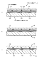
先ず、第1の実施形態について説明する。第1の実施形態は量子型赤外線検知器の一例に関する。図1は、第1の実施形態に係る赤外線検知器を示す斜視図であり、図2は、第1の実施形態に係る赤外線検知器を示す断面図である。
次に、第2の実施形態について説明する。第2の実施形態は赤外線検知器を含む撮像装置の一例に関する。図10は、第2の実施形態に係る撮像装置を示す図である。
読み出し回路アレイと、
前記読み出し回路アレイに実装された受光素子アレイと、
前記読み出し回路アレイと前記受光素子アレイとの間の固体電解質と、
を有し、
画素ごとに、前記固体電解質を間に挟むようにして、第1の電極が前記受光素子アレイに設けられ、第2の電極が前記読み出し回路アレイに設けられており、
前記第1の電極及び前記第2の電極のうちの一方が活性電極であり、他方が不活性電極であることを特徴とする赤外線検知器。
前記固体電解質はポリマー固体電解質であることを特徴とする付記1に記載の赤外線検知器。
前記第1の電極が不活性電極であり、第2の電極が活性電極であることを特徴とする付記1又は2に記載の赤外線検知器。
前記読み出し回路アレイは、前記第1の電極と前記第2の電極との間に電圧を印加して前記固体電解質中の金属架橋の生成及び消滅を制御するバイポーラ型の駆動回路を有することを特徴とする付記1乃至3のいずれか1項に記載の赤外線検知器。
前記駆動回路は、70K以上150K以下の第1の温度にて前記金属架橋を生成する電圧を印加することを特徴とする付記4に記載の赤外線検知器。
前記駆動回路は、前記金属架橋を生成する際に、読み出し時と同じ極性の電圧を印加することを特徴とする付記5に記載の赤外線検知器。
前記駆動回路は、273K以上の第2の温度にて前記金属架橋が消滅しているように電圧を印加することを特徴とする付記4に記載の赤外線検知器。
前記駆動回路は、前記金属架橋を消滅する際に、読み出し時と同じ極性の電圧を印加することを特徴とする付記7に記載の赤外線検知器。
前記第1の電極のピッチと前記第2の電極のピッチとが、70K以上150K以下の第1の温度にて実質的に一致することを特徴とする付記1乃至8のいずれか1項に記載の赤外線検知器。
前記活性電極はCu、Ag又はAlを含み、前記不活性電極はPd、Pt又はRuを含むことを特徴とする付記1乃至9のいずれか1項に記載の赤外線検知器。
(付記11)
付記1乃至9のいずれか1項に記載の赤外線検知器と、
前記赤外線検知器を冷却する冷却装置と、
を有することを特徴とする撮像装置。
110:受光素子アレイ
111:基板
112:受光素子
113:電極
120:読み出し回路アレイ
121:基板
123:電極
130、136、137:固体電解質
131:金属架橋
400:撮像装置
Claims (6)
- 読み出し回路アレイと、
前記読み出し回路アレイに実装された受光素子アレイと、
前記読み出し回路アレイと前記受光素子アレイとの間の固体電解質と、
を有し、
画素ごとに、前記固体電解質を間に挟むようにして、第1の電極が前記受光素子アレイに設けられ、第2の電極が前記読み出し回路アレイに設けられており、
前記第1の電極及び前記第2の電極のうちの一方が活性電極であり、他方が不活性電極であることを特徴とする赤外線検知器。 - 前記固体電解質はポリマー固体電解質であることを特徴とする請求項1に記載の赤外線検知器。
- 前記第1の電極が不活性電極であり、第2の電極が活性電極であることを特徴とする請求項1又は2に記載の赤外線検知器。
- 前記読み出し回路アレイは、前記第1の電極と前記第2の電極との間に電圧を印加して前記固体電解質中の金属架橋の生成及び消滅を制御するバイポーラ型の駆動回路を有することを特徴とする請求項1乃至3のいずれか1項に記載の赤外線検知器。
- 前記第1の電極のピッチと前記第2の電極のピッチとが、70K以上150K以下の第1の温度にて実質的に一致することを特徴とする請求項1乃至4のいずれか1項に記載の赤外線検知器。
- 請求項1乃至5のいずれか1項に記載の赤外線検知器と、
前記赤外線検知器を冷却する冷却装置と、
を有することを特徴とする撮像装置。
Priority Applications (1)
| Application Number | Priority Date | Filing Date | Title |
|---|---|---|---|
| JP2017000615A JP6823256B2 (ja) | 2017-01-05 | 2017-01-05 | 赤外線検知器及び撮像装置 |
Applications Claiming Priority (1)
| Application Number | Priority Date | Filing Date | Title |
|---|---|---|---|
| JP2017000615A JP6823256B2 (ja) | 2017-01-05 | 2017-01-05 | 赤外線検知器及び撮像装置 |
Publications (2)
| Publication Number | Publication Date |
|---|---|
| JP2018110194A true JP2018110194A (ja) | 2018-07-12 |
| JP6823256B2 JP6823256B2 (ja) | 2021-02-03 |
Family
ID=62844567
Family Applications (1)
| Application Number | Title | Priority Date | Filing Date |
|---|---|---|---|
| JP2017000615A Active JP6823256B2 (ja) | 2017-01-05 | 2017-01-05 | 赤外線検知器及び撮像装置 |
Country Status (1)
| Country | Link |
|---|---|
| JP (1) | JP6823256B2 (ja) |
Cited By (1)
| Publication number | Priority date | Publication date | Assignee | Title |
|---|---|---|---|---|
| JP2022147340A (ja) * | 2021-03-23 | 2022-10-06 | 住友電気工業株式会社 | 電子装置およびその製造方法 |
Citations (8)
| Publication number | Priority date | Publication date | Assignee | Title |
|---|---|---|---|---|
| JPH05281025A (ja) * | 1992-03-03 | 1993-10-29 | Fujitsu Ltd | 冷却型赤外線検知器及び冷却容器の製造方法 |
| JPH06181301A (ja) * | 1992-12-14 | 1994-06-28 | Fujitsu Ltd | 固体撮像素子 |
| JP2000091620A (ja) * | 1998-09-09 | 2000-03-31 | Fujitsu Ltd | Hg系II−VI族化合物半導体装置及びその製造方法 |
| JP2000512058A (ja) * | 1996-05-30 | 2000-09-12 | アクソン テクノロジーズ コーポレイション | プログラマブルメタライゼーションセル構造およびその作製方法 |
| JP2004235254A (ja) * | 2003-01-28 | 2004-08-19 | Fujitsu Ltd | 赤外線検出器及びその製造方法 |
| JP2010205858A (ja) * | 2009-03-02 | 2010-09-16 | Sumitomo Electric Ind Ltd | 光検出装置および光検出装置の製造方法 |
| JP2013251341A (ja) * | 2012-05-30 | 2013-12-12 | Sumitomo Electric Ind Ltd | 受光素子、半導体エピタキシャルウエハ、検出装置および受光素子の製造方法 |
| JP2015185771A (ja) * | 2014-03-25 | 2015-10-22 | 日本電気株式会社 | スイッチング素子およびスイッチング素子のプログラム方法 |
-
2017
- 2017-01-05 JP JP2017000615A patent/JP6823256B2/ja active Active
Patent Citations (8)
| Publication number | Priority date | Publication date | Assignee | Title |
|---|---|---|---|---|
| JPH05281025A (ja) * | 1992-03-03 | 1993-10-29 | Fujitsu Ltd | 冷却型赤外線検知器及び冷却容器の製造方法 |
| JPH06181301A (ja) * | 1992-12-14 | 1994-06-28 | Fujitsu Ltd | 固体撮像素子 |
| JP2000512058A (ja) * | 1996-05-30 | 2000-09-12 | アクソン テクノロジーズ コーポレイション | プログラマブルメタライゼーションセル構造およびその作製方法 |
| JP2000091620A (ja) * | 1998-09-09 | 2000-03-31 | Fujitsu Ltd | Hg系II−VI族化合物半導体装置及びその製造方法 |
| JP2004235254A (ja) * | 2003-01-28 | 2004-08-19 | Fujitsu Ltd | 赤外線検出器及びその製造方法 |
| JP2010205858A (ja) * | 2009-03-02 | 2010-09-16 | Sumitomo Electric Ind Ltd | 光検出装置および光検出装置の製造方法 |
| JP2013251341A (ja) * | 2012-05-30 | 2013-12-12 | Sumitomo Electric Ind Ltd | 受光素子、半導体エピタキシャルウエハ、検出装置および受光素子の製造方法 |
| JP2015185771A (ja) * | 2014-03-25 | 2015-10-22 | 日本電気株式会社 | スイッチング素子およびスイッチング素子のプログラム方法 |
Cited By (2)
| Publication number | Priority date | Publication date | Assignee | Title |
|---|---|---|---|---|
| JP2022147340A (ja) * | 2021-03-23 | 2022-10-06 | 住友電気工業株式会社 | 電子装置およびその製造方法 |
| JP7622493B2 (ja) | 2021-03-23 | 2025-01-28 | 住友電気工業株式会社 | 電子装置およびその製造方法 |
Also Published As
| Publication number | Publication date |
|---|---|
| JP6823256B2 (ja) | 2021-02-03 |
Similar Documents
| Publication | Publication Date | Title |
|---|---|---|
| Manda et al. | High-definition visible-SWIR InGaAs image sensor using Cu-Cu bonding of III-V to silicon wafer | |
| US9076702B2 (en) | Frontside-illuminated barrier infrared photodetector device and methods of fabricating the same | |
| JP2721146B2 (ja) | 共通の中間層金属コンタクトを有する2色赤外線同時検出器 | |
| US20090243016A1 (en) | Semiconductor device | |
| TW201448184A (zh) | 影像感測器裝置及其製造方法 | |
| TW201505162A (zh) | 穿孔於阻擋層以增強焦平面陣列之寬頻回應 | |
| JPWO2017126204A1 (ja) | 受光素子、受光素子の製造方法、撮像素子および電子機器 | |
| EP3894813B1 (fr) | Procede de realisation d'un detecteur infrarouge et detecteur infrarouge associe | |
| JP2010205858A (ja) | 光検出装置および光検出装置の製造方法 | |
| JP2011146603A (ja) | 検出装置、受光素子アレイ、電子機器、およびこれらの製造方法 | |
| JP6823256B2 (ja) | 赤外線検知器及び撮像装置 | |
| CN111213246B (zh) | 具有窄带隙半导体的异质结二极管 | |
| US20250022771A1 (en) | Image sensor with actively cooled sensor array | |
| JP2011096921A (ja) | 検出装置、センサ、および、これらの製造方法 | |
| US20240355949A1 (en) | Energy harvest and storage device for semiconductor chips and methods for forming the same | |
| Das et al. | Flip Chip Bonding of 68$\times $68 MWIR LED Arrays | |
| US10957659B2 (en) | Monolithic integration of III-V cells for powering memory erasure devices | |
| JP2018181957A (ja) | 撮像素子及び撮像装置 | |
| JP7666876B2 (ja) | 3d集積電気デバイス用の低応力誘電体層、平坦化方法、及び低温処理 | |
| JP2017157755A (ja) | 光検出器及び光検出器の製造方法 | |
| WO2023193280A1 (en) | Image sensor and electronic device including same | |
| KR101234340B1 (ko) | 이미지센서 모듈, 이를 포함하는 영상장치 및 이미지센서 모듈 제조방법 | |
| KR20180019269A (ko) | 반도체 장치 | |
| US9318517B1 (en) | Wafer level integration of focal plane arrays having a flexible conductive layer to provide an optical aperture for each pixel | |
| JP2023169730A (ja) | 光センサ、光センサの製造方法及び電子機器 |
Legal Events
| Date | Code | Title | Description |
|---|---|---|---|
| A621 | Written request for application examination |
Free format text: JAPANESE INTERMEDIATE CODE: A621 Effective date: 20190910 |
|
| A977 | Report on retrieval |
Free format text: JAPANESE INTERMEDIATE CODE: A971007 Effective date: 20200728 |
|
| A131 | Notification of reasons for refusal |
Free format text: JAPANESE INTERMEDIATE CODE: A131 Effective date: 20200804 |
|
| A521 | Request for written amendment filed |
Free format text: JAPANESE INTERMEDIATE CODE: A523 Effective date: 20201005 |
|
| TRDD | Decision of grant or rejection written | ||
| A01 | Written decision to grant a patent or to grant a registration (utility model) |
Free format text: JAPANESE INTERMEDIATE CODE: A01 Effective date: 20201208 |
|
| A61 | First payment of annual fees (during grant procedure) |
Free format text: JAPANESE INTERMEDIATE CODE: A61 Effective date: 20201221 |
|
| R150 | Certificate of patent or registration of utility model |
Ref document number: 6823256 Country of ref document: JP Free format text: JAPANESE INTERMEDIATE CODE: R150 |
|
| R250 | Receipt of annual fees |
Free format text: JAPANESE INTERMEDIATE CODE: R250 |
|
| R250 | Receipt of annual fees |
Free format text: JAPANESE INTERMEDIATE CODE: R250 |
|
| S111 | Request for change of ownership or part of ownership |
Free format text: JAPANESE INTERMEDIATE CODE: R313113 |
|
| R350 | Written notification of registration of transfer |
Free format text: JAPANESE INTERMEDIATE CODE: R350 |
|
| R250 | Receipt of annual fees |
Free format text: JAPANESE INTERMEDIATE CODE: R250 |