JP2018133473A - Semiconductor device manufacturing method and semiconductor device - Google Patents
Semiconductor device manufacturing method and semiconductor device Download PDFInfo
- Publication number
- JP2018133473A JP2018133473A JP2017026722A JP2017026722A JP2018133473A JP 2018133473 A JP2018133473 A JP 2018133473A JP 2017026722 A JP2017026722 A JP 2017026722A JP 2017026722 A JP2017026722 A JP 2017026722A JP 2018133473 A JP2018133473 A JP 2018133473A
- Authority
- JP
- Japan
- Prior art keywords
- substrate
- film
- thin film
- refractive index
- semiconductor device
- Prior art date
- Legal status (The legal status is an assumption and is not a legal conclusion. Google has not performed a legal analysis and makes no representation as to the accuracy of the status listed.)
- Withdrawn
Links
Images


Landscapes
- Testing Or Measuring Of Semiconductors Or The Like (AREA)
Abstract
Description
本発明は、半導体装置の製造方法および半導体装置に関する。 The present invention relates to a semiconductor device manufacturing method and a semiconductor device.
従来、ボロンシリサイド膜を拡散源として固相拡散法により不純物をシリコン基板にドーピングしていた(例えば、特許文献1参照)。
[先行技術文献]
[特許文献]
[特許文献1] 特開平7−183247号公報
Conventionally, a silicon substrate is doped with impurities by a solid phase diffusion method using a boron silicide film as a diffusion source (see, for example, Patent Document 1).
[Prior art documents]
[Patent Literature]
[Patent Document 1] JP-A-7-183247
シリコン基板へボロンを拡散して不純物領域を形成する場合、不純物領域が所望の不純物濃度で形成されたか否かを確認するべく、通常、BSG膜を除去して、四探針法等により当該不純物領域のシート抵抗を測定する。当該シート抵抗により、不純物領域の不純物濃度を推定することができる。しかしながら、四探針法等によりシート抵抗を測定する場合には、探針と不純物領域とを直接接触させる必要がある。また、工程管理用の基板が別途必要となるので、製造コストが上昇する。さらに、シート抵抗による不純物濃度の推定においては、不純物がオーバードーズされた場合にシリコン基板に生じた結晶欠陥を検知しにくいという問題がある。 When forming an impurity region by diffusing boron into a silicon substrate, the BSG film is usually removed to confirm whether the impurity region has been formed at a desired impurity concentration, and the impurity region is obtained by a four-probe method or the like. Measure the area sheet resistance. The impurity concentration in the impurity region can be estimated from the sheet resistance. However, when measuring the sheet resistance by the four-probe method or the like, it is necessary to directly contact the probe and the impurity region. In addition, since a process management substrate is required separately, the manufacturing cost increases. Furthermore, in the estimation of the impurity concentration by the sheet resistance, there is a problem that it is difficult to detect a crystal defect generated in the silicon substrate when the impurity is overdose.
本発明の第1の態様においては、半導体装置の製造方法を提供する。半導体装置は、シリコンを含む基板を有してよい。半導体装置の製造方法は、薄膜を基板上に形成し、かつ、基板を熱処理する段階と、薄膜の屈折率を測定する段階とを備えてよい。薄膜は、基板に対する不純物を含んでよい。薄膜を基板上に形成し、かつ、基板を熱処理する段階において、基板に不純物領域を形成してよい。不純物領域においては、薄膜から基板へ不純物が拡散されていてよい。 In a first aspect of the present invention, a method for manufacturing a semiconductor device is provided. The semiconductor device may have a substrate containing silicon. The method for manufacturing a semiconductor device may include a step of forming a thin film on the substrate, heat-treating the substrate, and measuring a refractive index of the thin film. The thin film may contain impurities for the substrate. In the step of forming a thin film on the substrate and heat-treating the substrate, impurity regions may be formed in the substrate. In the impurity region, impurities may be diffused from the thin film to the substrate.
半導体装置の製造方法は、薄膜の屈折率に基づいて、不純物領域のシート抵抗を推定する段階をさらに備えてよい。 The method for manufacturing a semiconductor device may further include a step of estimating the sheet resistance of the impurity region based on the refractive index of the thin film.
半導体装置の製造方法は、薄膜の屈折率に基づいて、不純物領域における不純物の濃度を推定する段階をさらに備えてよい。 The method for manufacturing a semiconductor device may further include a step of estimating the impurity concentration in the impurity region based on the refractive index of the thin film.
半導体装置の製造方法は、薄膜の屈折率に基づいて、基板の表面に生じた析出物の数を推定する段階をさらに備えてもよい。 The method for manufacturing a semiconductor device may further include a step of estimating the number of precipitates generated on the surface of the substrate based on the refractive index of the thin film.
さらに、半導体装置の製造方法は、薄膜の屈折率に基づいて、薄膜における不純物の濃度を推定する段階をさらに備えてもよい。 Furthermore, the method for manufacturing a semiconductor device may further include a step of estimating the impurity concentration in the thin film based on the refractive index of the thin film.
薄膜はPSG膜であってよい。また、不純物はリンであってよい。 The thin film may be a PSG film. The impurity may be phosphorus.
不純物領域は、1E+19cm−3以上1E+20cm−3未満の不純物濃度を有してよい。 The impurity region may have an impurity concentration of 1E + 19 cm −3 or more and less than 1E + 20 cm −3 .
薄膜の屈折率を測定する段階は、薄膜を基板上に形成し、かつ、基板を熱処理する段階の後であってよい。半導体装置の製造方法は、薄膜の屈折率を測定する段階の後に、薄膜の屈折率に基づいて、基板を追加的に熱処理する段階をさらに備えてよい。 Measuring the refractive index of the thin film may be after forming the thin film on the substrate and heat treating the substrate. The method for manufacturing a semiconductor device may further include a step of additionally heat-treating the substrate based on the refractive index of the thin film after the step of measuring the refractive index of the thin film.
薄膜の屈折率を測定する段階においては、基板の裏面の全面に接して設けられた薄膜の屈折率を測定してよい。 In the step of measuring the refractive index of the thin film, the refractive index of the thin film provided in contact with the entire back surface of the substrate may be measured.
本発明の第2の態様においては、半導体装置を提供する。半導体装置は、基板と、保護膜と、薄膜とを備えてよい。基板は、シリコンを含んでよい。保護膜は、基板よりも上に設けられてよい。薄膜は、基板に対する不純物を含んでよい。また、薄膜は、少なくとも一部が保護膜に覆われず、かつ、基板の上面視において矩形のリング状に設けられた不純物領域に接してよい。 In a second aspect of the present invention, a semiconductor device is provided. The semiconductor device may include a substrate, a protective film, and a thin film. The substrate may include silicon. The protective film may be provided above the substrate. The thin film may contain impurities for the substrate. Further, the thin film may be at least partially not covered with the protective film and may be in contact with the impurity region provided in a rectangular ring shape when the substrate is viewed from above.
薄膜は、300nm以下の厚みを有してよい。 The thin film may have a thickness of 300 nm or less.
なお、上記の発明の概要は、本発明の必要な特徴の全てを列挙したものではない。また、これらの特徴群のサブコンビネーションもまた、発明となりうる。 It should be noted that the above summary of the invention does not enumerate all the necessary features of the present invention. In addition, a sub-combination of these feature groups can also be an invention.
以下、発明の実施の形態を通じて本発明を説明するが、以下の実施形態は特許請求の範囲にかかる発明を限定するものではない。また、実施形態の中で説明されている特徴の組み合わせの全てが発明の解決手段に必須であるとは限らない。 Hereinafter, the present invention will be described through embodiments of the invention, but the following embodiments do not limit the invention according to the claims. In addition, not all the combinations of features described in the embodiments are essential for the solving means of the invention.
図1は、第1実施形態におけるダイオード100の(a)上面および(b)断面を示す図である。図1の(a)のA‐Aにおける断面が、図1の(b)に対応する。なお、理解を容易にすることを目的として、図1の(b)におけるマスク層20、BSG膜24、PSG膜、アノード電極30および保護膜35を図1の(a)では省略する。
FIG. 1 is a diagram illustrating a top surface and a (b) cross section of a
図1の(a)の上面図において、本例の半導体基板10はX軸およびY軸に平行な四辺を有する。X軸およびY軸は、互いに直交する軸である。なお、本例において、X‐Y平面は半導体基板10の裏面11および表(おもて)面19と平行である。Z軸は、X軸およびY軸と直交する。X軸方向、Y軸方向およびZ軸方向は、いわゆる右手系を成す。
In the top view of FIG. 1A, the
本明細書においては、Z軸の正方向を上と称し、Z軸の負方向を下と称する場合がある。また、Z軸の負方向を半導体基板10の深さ方向と称する場合がある。上および下は、基板、領域、層および膜等の相対的な位置関係を特定する便宜的な表現に過ぎない。例えば、Z軸方向は、必ずしも重力方向または地面に垂直な方向を意味しない。
In this specification, the positive direction of the Z-axis may be referred to as “up” and the negative direction of the Z-axis may be referred to as “down”. Further, the negative direction of the Z axis may be referred to as the depth direction of the
半導体基板10は、半導体チップであってよい。半導体基板10は、シリコンを含んでよい。本例の半導体基板10はシリコン基板であるが、半導体基板10は炭化ケイ素(SiC)基板であってもよい。本例の半導体基板10は、下部カソード領域12と、上部カソード領域14と、アノード領域16と、フィールドリミッティングリング(FLR)18とを有する。
The
下部カソード領域12および上部カソード領域14は、第1導電型の不純物領域である。本例において、第1導電型はn型である。本例の下部カソード領域12はn+型の不純物領域である。本例の下部カソード領域12は裏面11に露出する。
The
本例の下部カソード領域12は、n−型のシリコン基板の裏面11にn型不純物を拡散させることにより形成する。ただし、他の例においては、n+型の下部カソード領域12上にn−型のシリコン層をエピタキシャル成長させることにより、上部カソード領域14を形成してもよい。本例の上部カソード領域14は、n−型の不純物領域である。本例の上部カソード領域14は、下部カソード領域12上に設けられる。本例の上部カソード領域14の最上部は、X‐Y平面においてアノード領域16を囲むように表面19に露出する。
The
アノード領域16は、第2導電型の不純物領域である。本例において、第2導電型はp型である。本例のアノード領域16は、p+型の不純物領域である。本例のアノード領域16は、上部カソード領域14中に設けられる。本例のp+型のアノード領域16の最上部は、表面19に露出する。アノード領域16と上部カソード領域14との境界近傍には、pn接合が形成されてよい。
The
FLR18は、第1導電型の不純物領域である。本例のFLR18は、n+型の不純物領域である。FLR18は、上面視において矩形のリング状に設けられてよい。FLR18は、上面視においてアノード領域16よりも外側であり半導体基板10の外周よりも内側に設けられる。なお、FLR18の外周と半導体基板10の外周との間において、上部カソード領域14の一部が、表面19に露出する。
The
FLR18は、ダイオード100に逆バイアスが印加された場合に、アノード領域16と上部カソード領域14とのpn接合領域に形成される空乏層をX−Y平面方向に拡張させる機能を有してよい。FLR18を設けることにより、FLR18が設けられない場合と比較して、ダイオード100の逆バイアス耐圧を向上させることができる。
The
本例において、第1導電型はn型であり第2導電型はp型であるが、他の例においては、第1導電型がp型であり第2導電型がn型であってもよい。なお、nまたはpは、それぞれ電子または正孔が多数キャリアであることを意味する。nまたはpの右に記載した+または−について、+はそれが記載されていないものよりもキャリア濃度が高く、−はそれが記載されていないものよりもキャリア濃度が低いことを意味する。 In this example, the first conductivity type is n-type and the second conductivity type is p-type. However, in other examples, the first conductivity type is p-type and the second conductivity type is n-type. Good. Here, n or p means that electrons or holes are majority carriers, respectively. For + or − to the right of n or p, + means that the carrier concentration is higher than that where it is not described, and − means that the carrier concentration is lower than that where it is not described.
半導体装置としてのダイオード100は、半導体基板10と、マスク層20と、BSG(Borosilicate glass)膜24と、PSG(Phosphosilicate glss)膜28と、アノード電極30と、保護膜(パッシベーション膜)35と、カソード電極40とを備える。アノード電極30は、アノード領域16上に設けられ、アノード領域16の最上部と直接接してよい。なお、アノード電極30は、上部カソード領域14には直接接しなくてよい。
The
マスク層20は、半導体基板10に直接接して、半導体基板10の表面19上に設けられる。本例のマスク層20は、二酸化シリコン(SiO2)層である。BSG膜24は、マスク層20に直接接して、マスク層20上に設けられる。
The
マスク層20は、気相拡散法における不純物源と半導体基板10の表面19とが接触する領域を定めることを目的として用いられてよい。マスク層20で覆われた領域において、マスク層20から下方には不純物が拡散しないとしてよい。ただし、マスク層20と同じ高さに位置する不純物源からX‐Y平面方向に不純物が拡散して、マスク層20の下に入り込むことは許容されてもよい。
The
BSG膜24は、ダイオード100の製造過程において、半導体基板10に対するp型不純物であるボロンを供給する供給源として機能してよい。BSG膜24は、ダイオード100の製造後において、層間絶縁膜として機能してよい。
The
PSG膜28は、表面19およびBSG膜24に直接接して、表面19およびBSG膜24上に設けられる。PSG膜28は、ダイオード100の製造過程において、半導体基板10に対するn型不純物であるリンを供給する供給源として機能してよい。PSG膜28も、ダイオード100の製造後において、層間絶縁膜として機能してよい。
The
保護膜35は、半導体基板10よりも上に設けられてよい。保護膜35は、ダイオード100の最上部に設けられてよい。本例の保護膜35は、PSG膜28およびアノード電極30上に設けられる。保護膜35は、アノード電極30上に開口37を有してよい。アノード端子は、開口37を介してアノード電極30に接続することができる。
The
本例のカソード電極40は、下部カソード領域12の下に設けられ、裏面11と直接接する。カソード端子は、カソード電極40に接続してよい。
The
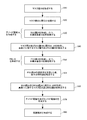
図2は、ダイオード100を製造するための各段階を示すフロー図である。本例においては、段階S10〜S60の順に(即ち、番号が若い順に)、各段階が実行される。
FIG. 2 is a flow diagram illustrating the steps for manufacturing the
図3は、ダイオード100を製造するための各段階を示す図である。説明を容易にすることを目的として、図3においては、各段階におけるダイオード100の断面を示す。図3のS10〜S80は、図2のS10〜S80に対応する。なお、図3の各段階は、ダイオード100がウェハからダイシングされてチップとなる前の状況を示す。それゆえ、図3の説明においては、半導体基板10をウェハと読み替えてもよい。
FIG. 3 is a diagram illustrating steps for manufacturing the
S10は、半導体基板10の表面19上にマスク層20を形成する段階である。マスク層20は、半導体基板10の裏面11および表面19を覆ってよい。マスク層20は、半導体基板10を熱酸化することにより形成される熱酸化膜であってよい。熱酸化膜は二酸化シリコン(SiO2)膜と見なしてよい。
S <b> 10 is a step of forming a
S20は、マスク層20に開口21を設ける段階である。開口21は、既知のフォトリソグラフィーおよびエッチング技術を利用して形成されてよい。開口21は、表面19の一部の領域を露出させてよい。本例の開口21は、アノード領域16に対応する領域に予め定められた形状を有する。つまり、開口21が、表面19におけるアノード領域16の外形を規定してよい。マスク層20に開口21が存在することにより、BSG膜24を表面19およびマスク層20上に形成することで、BSG膜24と表面19との接触領域を規定することができる。
S <b> 20 is a step of providing an
S30は、BSG膜24を形成し、かつ、半導体基板10を熱処理する段階である。つまり、本例のS30は、BSG膜24を形成する段階と、半導体基板10を熱処理する段階とを含む。本例では、複数の半導体基板10の各々の側面を石英ボートに固定することにより、当該複数の半導体基板10を横型CVD装置のチャンバ内部に配置する。チャンバ内部および半導体基板10の温度は、横型CVD装置に備え付けられたヒーターにより調節可能であってよい。
S30 is a stage in which the
本例では、原料ガスをチャンバ内部に導入することにより、半導体基板10の周囲にBSG膜24を形成する。例えば、三臭化ホウ素(BBr3)および酸素(O2)を含む原料ガスをチャンバ内部に導入する。BBr3およびO2はBSG膜24の形成材料であり、BBr3はp型不純物であるボロンの気相拡散源でもある。当該原料ガスをチャンバ内部に導入するとき、チャンバ内部の温度は1000℃以上1100℃以下としてよい。また、当該原料ガスをチャンバ内部に導入してBSG膜24を成膜する時間は、30分としてよい。
In this example, the
チャンバ内部に導入する原料ガスの流量は、マスフローコントローラ(MFC)により制御してよい。BSG膜24の厚みは、10nm以上300nm以下としてよい。本例のBSG膜24の厚みは、100nm以上200nm以下とする。当業者であれば、BSG膜24の厚みと混合ガスの導入時間とに基づいて、混合ガスの流量を適宜決定することができる。本例において、BSG膜24は半導体基板10の両面に形成される。より具体的には、BSG膜24は、マスク層20および表面19上に形成され、かつ、裏面11の下にも形成される。
The flow rate of the source gas introduced into the chamber may be controlled by a mass flow controller (MFC). The thickness of the
BSG膜24の形成およびその直後における半導体基板10の熱処理において、チャンバ内部の温度は同じであってよい。本例においては、原料ガスをチャンバ内部に導入することを止めた後に、所定の温度で所定時間、半導体基板10を熱処理してよい。本例においては、1000℃以上1100℃以下の所定の温度で5時間以上10時間以下の所定時間、半導体基板10を熱処理する。一連のBSG膜24形成および熱処理により、BSG膜24から半導体基板10へp型不純物が拡散された不純物領域であるアノード領域16を形成する。このように、本例においては、気相拡散法によりBSG膜24およびアノード領域16を形成する。なお、裏面11の下は、マスク層20により全面が覆われているので、p型不純物は裏面11には拡散しない。
In the formation of the
本例のアノード領域16は、1E+19cm−3以上1E+20cm−3未満のp型不純物濃度を有する。なお、Eは10のべき乗を意味する。例えば、1E+19は、1×10¹⁹を意味する。不純物濃度を上記範囲とすることで、不純物濃度をある程度高くしつつも、不純物濃度を半導体基板10の固溶限界の範囲内とすることができる。
The
不純物濃度が半導体基板10の固溶限界を超えると(即ち、不純物が半導体基板10にオーバードーズされると)、不純物が半導体基板10に析出する。析出物は、結晶欠陥として機能し得る。なお、本例において、結晶欠陥とは目視検出可能な析出物を意味する。
When the impurity concentration exceeds the solid solution limit of the semiconductor substrate 10 (that is, when the impurity is overdose into the semiconductor substrate 10), the impurity is deposited on the
S40は、マスク層20およびBSG膜24に開口22および25を形成し、裏面11に接するマスク層20およびBSG膜24を除去する段階である。本例では、既知のエッチング技術を利用して、マスク層20に開口22を形成し、BSG膜24に開口25を形成する。開口22は表面19に達し、開口25は開口22に達する。開口22および開口25は、一つながりのコンタクトホールを構成してよい。また、S40において、既知のエッチング技術を利用して、裏面11下のマスク層20およびBSG膜24を全て除去する。
S40 is a stage in which
S50は、PSG膜28を形成し、かつ、半導体基板10を熱処理する段階である。つまり、本例のS50は、S30と同様に、PSG膜28を形成する段階と、半導体基板10を熱処理する段階とを含む。S30と同様に、横型CVD装置を用いて、PSG膜28を形成してよい。なお、PSG膜28は、薄膜の一例である。
S50 is a stage in which the
PSG膜28を形成する原料ガスは、例えば、塩化ホスホリル(POCl3)および酸素(O2)を含んでよい。POCl3およびO2はPSG膜28の形成材料であり、POCl3はn型不純物であるリンの気相拡散源でもある。PSG膜28の厚みは、10nm以上300nm以下としてよい。10nmという厚みは、自然酸化膜よりも厚いので、製造プロセスにおいて形成された膜厚であるとみなしてよい。本例のPSG膜28の厚みは、100nm以上200nm以下とする。PSG膜28の形成およびその直後における半導体基板10の熱処理において、チャンバ内部の温度および処理時間は同じであってよい。チャンバ内部の温度は950℃以上1050℃以下としてよく、原料ガスをチャンバ内部に導入してPSG膜28を成膜する時間は、1時間以上2時間以下としてよい。本例においては、チャンバ内部の温度は1000℃とし、PSG膜28を成膜する時間は1時間30分とする。原料ガスの導入を止めた後、950℃以上1100℃以下の所定の温度で1時間以上2時間以下の所定時間、半導体基板10を熱処理してよい。本例においては、原料ガスの導入を止めた後、1000℃で1時間30分、半導体基板10を熱処理する。
The source gas for forming the
本例では、PSG膜28を形成し、かつ、熱処理することにより、気相拡散法でFLR18および下部カソード領域12を形成する。S50において、裏面11の下はPSG膜28により全面が覆われることにより、裏面11から半導体基板10の所定の深さ位置まで下部カソード領域12が形成される。なお、FLR18は、薄膜から半導体基板10へ不純物が拡散された不純物領域の一例である。
In this example, the
S54は、PSG膜28の屈折率を測定し、その後、種々の特性値を推定する段階である。つまり、S54は、屈折率の測定する段階と、特性値を推定する段階との二つの段階を含む。
S54 is a stage in which the refractive index of the
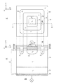
本例においては、横型CVD装置内の複数の半導体基板10のうち少なくとも1つの半導体基板10をチャンバから取り出し、PSG膜28の屈折率を測定する。また、本例においては、レーザー光源110および受光部120を有するエリプソメータによりPSG膜28の屈折率を測定する。レーザー光源110および受光部120を用いることにより、PSG膜28に非接触で、直径数百μmの微小領域におけるPSG膜28の屈折率を測定することができる。なお、PSG膜28の屈折率を非接触で測定することができれば、偏光解析法(エリプソメトリー)に限らず他の測定方法を用いてもよい。
In this example, at least one
種々の特性値は、PSG膜28の不純物濃度と、FLR18のシート抵抗と、FLR18の不純物濃度と、FLR18の析出物の数とを含んでよい。つまり、種々の特性値を推定する段階は、PSG膜28の屈折率に基づいて、PSG膜28におけるn型の不純物濃度を推定する段階と、FLR18のシート抵抗を推定する段階と、FLR18におけるn型の不純物濃度を推定する段階と、FLR18が設けられた領域における半導体基板10の表面19に生じた析出物の数を推定する段階との一以上の段階を含んでよい。
The various characteristic values may include the impurity concentration of the
PSG膜28の屈折率は、PSG膜28中のn型不純物濃度に応じて変化してよい。本例では、PSG膜28中のn型不純物濃度が高いほどPSG膜28の屈折率は高く、PSG膜28中のn型不純物濃度が低いほどPSG膜28の屈折率は低い。
The refractive index of the
また、FLR18の不純物濃度は、不純物源であるPSG膜28中の不純物濃度に応じて変化してよい。本例では、PSG膜28中のn型不純物濃度が高いほどFLR18のn型不純物濃度が高く、PSG膜28中のn型不純物濃度が低いほどFLR18のn型不純物濃度が低い。FLR18の不純物濃度は、PSG膜28中のn型不純物濃度に指数関数的に比例してよい。
Further, the impurity concentration of the
PSG膜28の屈折率と、PSG膜28のn型不純物濃度との第1の対応関係を測定したテーブルまたはグラフ等を予め取得しておくことにより、PSG膜28の屈折率を測定することで、PSG膜28の不純物濃度を推定することができる。また、予め取得した第1の対応関係を利用することにより、PSG膜28の屈折率を測定することで、FLR18の不純物濃度を推定することもできる。
By obtaining in advance a table or graph that measures the first correspondence between the refractive index of the
FLR18において、n型不純物濃度とシート抵抗とは負の相関関係がある。FLR18においてn型不純物濃度が高いほどシート抵抗は低く、n型不純物濃度が低いほどシート抵抗は高い。PSG膜28の屈折率と、FLR18におけるn型不純物濃度およびシート抵抗との第2の対応関係を測定したテーブルまたはグラフを予め取得しておくことにより、PSG膜28の屈折率を測定することで、FLR18におけるシート抵抗を推定することができる。
In
このように、本例では、FLR18に接触することなく、FLR18のシート抵抗を推定することができる。それゆえ、本例においては、四探針法等により不純物領域のシート抵抗を測定する場合と異なり、探針と不純物領域とを直接接触させる必要がない。また、本例においては、屈折率を測定するときに表面19上のマスク層20、BSG膜24およびPSG膜28等を剥離しなくてよいので、シート抵抗の推定に要する作業が四探針法等に比べて容易である。さらに、本例では、探針をFLR18に接触させる精密な作業も不要である。それゆえ、シート抵抗の推定に要する作業時間も四探針法等に比べて短縮することができる。
Thus, in this example, the sheet resistance of the
加えて、本例においては、四探針法等により不純物領域のシート抵抗を測定する場合と異なり、工程管理用の半導体基板10そのものが不要である。つまり、最終製品となる半導体基板10をシート抵抗の推定に用いることができる。それゆえ、工程管理用の半導体基板10を用いる場合に比べて、ダイオード100の製造コストを低減することができる。
In addition, in this example, unlike the case where the sheet resistance of the impurity region is measured by the four-probe method or the like, the
さらに本例では、屈折率を測定することにより、表面19に析出した結晶欠陥の数を推定することができる。当該推定方法は、四探針法等に比べて非常に容易に析出物の数を推定することができる。結晶欠陥は、表面19に析出したBSG、PSGまたはBPSG(Borophosphosilicate glss)であってよい。本例の結晶欠陥はBPSGの塊である。
Furthermore, in this example, the number of crystal defects deposited on the
結晶欠陥は、FLR18に生じる可能性がある。本例では、1E+19cm−3以上1E+20cm−3未満のp型不純物濃度を有するアノード領域16を形成する際に、非常に高濃度のp型不純物を有するBSG膜24を形成した。製造工程中に、ボロンはPSG膜28に混入しFLR18中へと拡散する場合がある。半導体基板10がシリコン基板の場合、1E+20cm−3が固溶限界であると考えてよい。それゆえ、n型不純物およびp型不純物の不純物濃度の合計が1E+20cm−3を超えるとシリコン基板に結晶欠陥が生じ得る。結晶欠陥は、半導体素子の特性不良を引き起こす可能性がある。それゆえ、所定数以上の結晶欠陥を有する半導体基板10は、分別することが望ましい。
Crystal defects can occur in the
半導体基板10に結晶欠陥が生じた場合の屈折率と生じなかった場合の屈折率との差は、半導体基板10に結晶欠陥が生じた場合のシート抵抗と生じなかった場合のシート抵抗との差に比べて、ずっと把握しやすい(後述の図4およびその説明も参照されたい)。それゆえ、四探針法等によりシート抵抗を測定して結晶欠陥の数を推定する場合に比べて、屈折率を測定することにより結晶欠陥の数を推定する方が、より容易にかつ正しく結晶欠陥の数を推定することができる。
The difference between the refractive index when the crystal defect occurs in the
一例において、結晶欠陥の検出方法として、光学顕微鏡等により作業者が半導体基板10の結晶欠陥を目視で検査することが考えられる。これに対して本例では、屈折率を測定することにより、表面19に生じた結晶欠陥の数を推定することができるので、目視検査に比べてより短時間で正確に結晶欠陥の数を推定することができる。これにより、半導体基板10を捨てるべきかまたは次の段階で使用するかについて、正確な判断が行いやすくなるという利点がある。
In one example, as a method for detecting a crystal defect, it is conceivable that an operator visually inspects the crystal defect of the
なお、結晶欠陥は、PSG膜28が接するn+型の下部カソード領域12にも生じ得る。それゆえ、FLR18上に設けられたPSG膜28の屈折率を測定することに加えて、またはこれに代えて、裏面11の裏面の全面に接して設けられたPSG膜28の屈折率を測定してもよい。横型CVD装置のチャンバ内において隣接する半導体基板10からボロンが混入した場合、下部カソード領域12の裏面11近傍にも結晶欠陥が生じ得る。PSG膜28は裏面11下の全面に設けられるので、FLR18上におけるPSG膜28に比べて測定領域が広い。それゆえ、PSG膜28の屈折率がより容易である。
Crystal defects may also occur in the n + -type
S60は、BSG膜24およびPSG膜28に開口23、29を形成し、裏面11に接するPSG膜28を除去する段階である。本例では、既知のエッチング技術を利用して、BSG膜24に開口23を形成し、PSG膜28に開口29を形成する。開口23は表面19(アノード16)に達し、開口29は開口23に達する。開口23および開口29は、一つながりのコンタクトホールを構成してよい。また、既知のエッチング技術を利用して、裏面11下のPSG膜28を全て除去する。
S60 is a stage in which
S70は、アノード電極30およびカソード電極40を形成する段階である。本例では、表面19およびPSG膜28上にアノード電極30を形成した後、アノード領域16上のみにアノード電極30を残すようにアノード電極30の一部をエッチングにより除去する。その後、裏面11の下の全体にカソード電極40を形成する。なお、カソード電極40を形成した後に、アノード電極30を形成してもよい。
S70 is a stage in which the
S80は、保護膜35を形成する段階である。本例では、アノード電極30およびPSG膜28上に保護膜35を形成した後、アノード電極30上のみに開口37を形成するように保護膜35の一部をエッチングにより除去する。
S80 is a stage in which the
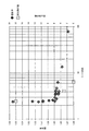
図4は、シート抵抗に対する屈折率および析出物の数を測定した実験結果を示す図である。まず、気相拡散法によりFLR18を形成した各サンプルのPSG膜28の屈折率を測定した。また、PSG膜28を除去して各サンプルのFLR18のシート抵抗を四端子法により測定した。また、いくつかのサンプルについては、光学顕微鏡を用いて表面19に生じた析出物の数を目視によりカウントした。
FIG. 4 is a diagram showing experimental results obtained by measuring the refractive index with respect to the sheet resistance and the number of precipitates. First, the refractive index of the
横軸は対数目盛で表示されたシート抵抗(Ω/□)である。左の縦軸は、PSG膜28の屈折率である。右の縦軸は、表面19における25mm×25mm四方に生じた析出物の数である。図4において、屈折率をひし形で示し、析出物の数を正方形で示す。
The horizontal axis is the sheet resistance (Ω / □) displayed on a logarithmic scale. The vertical axis on the left is the refractive index of the
本実験結果によれば、シート抵抗が高いサンプルほど屈折率が小さく、シート抵抗が低いサンプルほど屈折率が大きいことが観測された。シート抵抗が約2.2(Ω/□)の近傍において、屈折率は急激に変化した。また、シート抵抗3.0(Ω/□)から100(Ω/□)にかけて、屈折率は徐々に減少した。このように、シート抵抗と屈折率との間には、明確な負の相関関係があった。 According to the results of this experiment, it was observed that the sample with higher sheet resistance has a lower refractive index, and the sample with lower sheet resistance has a higher refractive index. In the vicinity of the sheet resistance of about 2.2 (Ω / □), the refractive index changed rapidly. Further, the refractive index gradually decreased from a sheet resistance of 3.0 (Ω / □) to 100 (Ω / □). Thus, there was a clear negative correlation between sheet resistance and refractive index.
シート抵抗と析出物の数との間にも、負の相関関係があった。シート抵抗が低いほどFLR18の不純物濃度が相対的に高く、これに応じて析出物の数も相対的に多いと考えられる。また、シート抵抗が高いほどFLR18の不純物濃度が相対的に低く、これに応じて析出物の数も相対的に少ないと考えられる。
There was also a negative correlation between sheet resistance and the number of precipitates. It is considered that the lower the sheet resistance, the higher the impurity concentration of
シート抵抗が約2.2(Ω/□)のサンプルでは析出物の数は18であり、シート抵抗が約4.1(Ω/□)のサンプルでは析出物の数は3であり、シート抵抗が約6.2(Ω/□)のサンプルでは析出物の数は0であった。このように、数(Ω/□)のシート抵抗の変化において析出物の数は急激に変化した。このように、シート抵抗が僅かに変化するに中で、シート抵抗の測定により析出物の数を推定することは難しい。 In the sample having a sheet resistance of about 2.2 (Ω / □), the number of precipitates is 18, and in the sample having a sheet resistance of about 4.1 (Ω / □), the number of precipitates is 3, and the sheet resistance is about 6. In the sample of 2 (Ω / □), the number of precipitates was zero. Thus, the number of precipitates changed abruptly when the sheet resistance changed by several (Ω / □). As described above, it is difficult to estimate the number of precipitates by measuring the sheet resistance while the sheet resistance slightly changes.
これに対して、屈折率の変化は析出物の数の変化に応じて急激に変化することが図4から明らかである。それゆえ、屈折率を測定することにより析出物の数を推定することで、四端子法によりシート抵抗を測定する場合に比べて、より敏感に析出物の発生を推定することができる。つまり、屈折率は、シート抵抗に比べて析出物の発生を検出することについて優れている。 On the other hand, it is clear from FIG. 4 that the change in the refractive index changes rapidly according to the change in the number of precipitates. Therefore, by estimating the number of precipitates by measuring the refractive index, it is possible to estimate the generation of precipitates more sensitively than when measuring the sheet resistance by the four probe method. That is, the refractive index is superior for detecting the occurrence of precipitates compared to the sheet resistance.
上述のように、半導体基板10がシリコン基板である場合に、例えば、FLR18における不純物濃度の合計が1E+20cm−3を超えると、結晶欠陥が生じ得る。一例において、半導体基板10の特定の領域に5E+19cm−3のボロンがドープされ、かつ、6E+19cm−3のリンがドープされることにより、当該特定の領域に合計で1.1E+20cm−3の不純物がドープされる。これにより、当該特定の領域に結晶欠陥が生じ得る。
As described above, when the
図5は、第1実施形態の第1変形例におけるフロー図である。本例においては、S54の後に、半導体基板10を追加的に熱処理する段階(S56)を更に備える。係る点が、第1実施形態と異なる。他の点は、第1実施形態と同じである。
FIG. 5 is a flowchart in the first modification of the first embodiment. In this example, a step (S56) of additionally heat-treating the
本例においては、屈折率の測定(S54)において得られたPSG膜28の屈折率に基づいて、半導体基板10を追加的に熱処理(S56)する。例えば、S54で測定されたPSG膜28の不純物濃度が予め定められた値よりも低いと推定される場合には、追加熱処理(S56)の温度を高く、および/または、追加熱処理(S56)の時間を長くする。
In this example, the
これにより、PSG膜28から半導体基板10へ拡散する不純物を増加させて、FLR18の不純物濃度を設計値に近づける、または、一致させることができる。つまり、PSG膜28における不純物濃度の設計値からのずれを次段階において補うことができる。これにより、ダイオード100の品質を管理し易くなるので有利である。
Thereby, impurities diffused from the
上述の第1実施形態およびその変形例においては、n+型のFLR18を形成するべく、PSG膜28を形成する例を示した。ただし、他の例においては、PSG膜28を用いて、n型またはn−型のFLR18を形成してもよい。また、さらなる他の例においては、p型またはp+型のFLR18を形成するべくBSG膜24を形成する場合においても、PSG膜28をBSG膜に変更した上で、第1実施形態およびその変形例を適用してよい。
In the above-described first embodiment and its modifications, the example in which the
図6は、第2実施形態におけるダイオード200の(a)上面および(b)断面を示す図である。図6の(a)のB‐Bにおける断面が、図6の(b)に対応する。なお、図1と同様に、図6(b)におけるマスク層20、BSG膜24、PSG膜、アノード電極30および保護膜35を、図6の(a)では省略する。
FIGS. 6A and 6B are diagrams showing a (a) top surface and a (b) cross section of the
本例の保護膜35は、FLR18の上方に開口38を有する。開口38は、少なくとも一部が保護膜35に覆われず、かつ、FLR18に接するPSG膜28を外部に露出する。係る点において、本例は、第1実施形態と異なる。なお、図6(a)においては、保護膜35の開口37および開口38の外形を点線で示す。
The
本例においては、ダイオード200の完成後において、PSG膜28の屈折率を測定することができる。それゆえ、PSG膜28の屈折率に基づいて、PSG膜28におけるn型の不純物の濃度の推定と、FLR18のシート抵抗の推定と、FLR18におけるn型の不純物濃度の推定と、半導体基板10の表面19に生じた析出物の数の推定との一以上を行うことができる。つまり、ダイオード200の製造後においても、ダイオード200の不良解析ができる点が有利である。
In this example, the refractive index of the
PSG膜28の厚みは、300nm以下である。これに対して、半導体デバイスに通常用いられる層間絶縁膜は1μm程度の厚みを有する。1μm程度の厚みに対しては、屈折率の測定が難しい場合がある。これに対して、本例のPSG膜28は、通常の層間絶縁膜よりも十分に薄いので、確実に屈折率を測定することができる。
The thickness of the
上記における半導体装置の例はダイオードのみであるが、本願の技術は、ダイオード以外の半導体装置に適用されてもよい。本願の技術は、IGBT(Insulated Gate Bipolar Transistor)、MOSFET(Metal Oxide Semiconductor Field Effect Transistor)、IGBTとFWD(Free Wheeling Diode)とを内蔵したRC‐IGBT(Reverse Conducting IGBT)に適用されてもよい。 Although the example of the semiconductor device in the above is only a diode, the technique of the present application may be applied to a semiconductor device other than the diode. The technology of the present application is an IGBT (Insulated Gate Bipolar Transistor), a MOSFET (Metal Oxide Field Transistor Transistor), an IGBT and a FWD (Free Wheeling Diode), which is a B-based RC.
以上、本発明を実施の形態を用いて説明したが、本発明の技術的範囲は上記実施の形態に記載の範囲には限定されない。上記実施の形態に、多様な変更又は改良を加えることが可能であることが当業者に明らかである。その様な変更又は改良を加えた形態も本発明の技術的範囲に含まれ得ることが、特許請求の範囲の記載から明らかである。 As mentioned above, although this invention was demonstrated using embodiment, the technical scope of this invention is not limited to the range as described in the said embodiment. It will be apparent to those skilled in the art that various modifications or improvements can be added to the above embodiment. It is apparent from the description of the scope of claims that embodiments with such changes or improvements can be included in the technical scope of the present invention.
特許請求の範囲、明細書、および図面中において示した装置、システム、プログラム、および方法における動作、手順、ステップ、および段階等の各処理の実行順序は、特段「より前に」、「先立って」等と明示しておらず、また、前の処理の出力を後の処理で用いるのでない限り、任意の順序で実現しうることに留意すべきである。特許請求の範囲、明細書、および図面中の動作フローに関して、便宜上「まず、」、「次に、」等を用いて説明したとしても、この順序で実施することが必須であることを意味するものではない。 The order of execution of each process such as operations, procedures, steps, and stages in the apparatus, system, program, and method shown in the claims, the description, and the drawings is particularly “before” or “prior to”. It should be noted that the output can be realized in any order unless the output of the previous process is used in the subsequent process. Even if the operation flow in the claims, the description, and the drawings is described using “first”, “next”, etc. for convenience, it means that it is essential to carry out in this order. It is not a thing.
10・・半導体基板、11・・裏面、12・・下部カソード領域、14・・上部カソード領域、16・・アノード領域、18・・FLR、19・・表面、20・・マスク層、21・・開口、22・・開口、23・・開口、24・・BSG膜、25・・開口、28・・PSG膜、29・・開口、30・・アノード電極、35・・保護膜、37・・開口、38・・開口、40・・カソード電極、100・・ダイオード、110・・レーザー光源、120・・受光部、200・・ダイオード 10..Semiconductor substrate, 11..Back surface, 12..Lower cathode region, 14..Upper cathode region, 16..Anode region, 18..FLR, 19..Front surface, 20..Mask layer, 21 .. Aperture, 22 ... aperture, 23 ... aperture, 24 ... BSG film, 25 ... aperture, 28 ... PSG film, 29 ... aperture, 30 ... anode electrode, 35 ... protective film, 37 ... aperture , 38 .. Opening, 40 .. Cathode electrode, 100 .. Diode, 110 .. Laser light source, 120 .. Light receiving part, 200.
Claims (11)
前記基板に対する不純物を含む薄膜を前記基板上に形成し、かつ、前記薄膜から前記基板へ前記不純物が拡散された不純物領域を前記基板に形成するべく前記基板を熱処理する段階と、
前記薄膜の屈折率を測定する段階と
を備える
半導体装置の製造方法。 A method of manufacturing a semiconductor device having a substrate containing silicon,
Forming a thin film including impurities on the substrate on the substrate, and heat-treating the substrate to form an impurity region on the substrate in which the impurities are diffused from the thin film to the substrate;
Measuring the refractive index of the thin film.
請求項1に記載の半導体装置の製造方法。 The method for manufacturing a semiconductor device according to claim 1, further comprising estimating a sheet resistance of the impurity region based on the refractive index of the thin film.
請求項1または2に記載の半導体装置の製造方法。 The method for manufacturing a semiconductor device according to claim 1, further comprising estimating a concentration of the impurity in the impurity region based on the refractive index of the thin film.
請求項1から3のいずれか一項に記載の半導体装置の製造方法。 4. The method of manufacturing a semiconductor device according to claim 1, further comprising estimating a number of precipitates generated on the surface of the substrate based on the refractive index of the thin film.
請求項1から4のいずれか一項に記載の半導体装置の製造方法。 5. The method of manufacturing a semiconductor device according to claim 1, further comprising estimating a concentration of the impurity in the thin film based on the refractive index of the thin film.
請求項1から5のいずれか一項に記載の半導体装置の製造方法。 The method for manufacturing a semiconductor device according to claim 1, wherein the thin film is a PSG film, and the impurity is phosphorus.
請求項1から6のいずれか一項に記載の半導体装置の製造方法。 The method for manufacturing a semiconductor device according to claim 1, wherein the impurity region has an impurity concentration of 1E + 19 cm −3 or more and less than 1E + 20 cm −3 .
前記薄膜の前記屈折率を測定する段階の後に、前記薄膜の前記屈折率に基づいて、前記基板を追加的に熱処理する段階をさらに備える
請求項1から7のいずれか一項に記載の半導体装置の製造方法。
Measuring the refractive index of the thin film is after forming the thin film on the substrate and heat treating the substrate;
The semiconductor device according to claim 1, further comprising a step of additionally heat-treating the substrate based on the refractive index of the thin film after the step of measuring the refractive index of the thin film. Manufacturing method.
請求項1から8のいずれか一項に記載の半導体装置の製造方法。 The method for manufacturing a semiconductor device according to claim 1, wherein in the step of measuring the refractive index of the thin film, the refractive index of the thin film provided in contact with the entire back surface of the substrate is measured.
シリコンを含む基板と、
前記基板よりも上に設けられた保護膜と、
少なくとも一部が前記保護膜に覆われず、かつ、前記基板の上面視において矩形のリング状に設けられた不純物領域に接し、前記基板に対する不純物を含む薄膜と
を備える
半導体装置。 A semiconductor device,
A substrate containing silicon;
A protective film provided above the substrate;
A semiconductor device comprising: a thin film that is not covered with the protective film and is in contact with an impurity region provided in a rectangular ring shape in a top view of the substrate and includes an impurity with respect to the substrate.
請求項10に記載の半導体装置。 The semiconductor device according to claim 10, wherein the thin film has a thickness of 300 nm or less.
Priority Applications (1)
| Application Number | Priority Date | Filing Date | Title |
|---|---|---|---|
| JP2017026722A JP2018133473A (en) | 2017-02-16 | 2017-02-16 | Semiconductor device manufacturing method and semiconductor device |
Applications Claiming Priority (1)
| Application Number | Priority Date | Filing Date | Title |
|---|---|---|---|
| JP2017026722A JP2018133473A (en) | 2017-02-16 | 2017-02-16 | Semiconductor device manufacturing method and semiconductor device |
Publications (1)
| Publication Number | Publication Date |
|---|---|
| JP2018133473A true JP2018133473A (en) | 2018-08-23 |
Family
ID=63248611
Family Applications (1)
| Application Number | Title | Priority Date | Filing Date |
|---|---|---|---|
| JP2017026722A Withdrawn JP2018133473A (en) | 2017-02-16 | 2017-02-16 | Semiconductor device manufacturing method and semiconductor device |
Country Status (1)
| Country | Link |
|---|---|
| JP (1) | JP2018133473A (en) |
Citations (7)
| Publication number | Priority date | Publication date | Assignee | Title |
|---|---|---|---|---|
| JPS5818976A (en) * | 1981-07-27 | 1983-02-03 | Semiconductor Energy Lab Co Ltd | Photoelectric conversion device manufacturing method |
| JPH0755702A (en) * | 1993-08-12 | 1995-03-03 | Hitachi Ltd | Crystal defect measuring apparatus and semiconductor manufacturing apparatus using the same |
| JPH11214391A (en) * | 1998-01-21 | 1999-08-06 | Yamaha Corp | Titanium oxide and nitride film evaluation method and wiring formation method therefor |
| JP2002540396A (en) * | 1999-03-22 | 2002-11-26 | ボクサー・クロス・インコーポレイテッド | Apparatus and method for determining active dopant profile of semiconductor wafer |
| JP2013533959A (en) * | 2010-06-04 | 2013-08-29 | アイメック | Method for determining the active doping concentration of doped semiconductor regions |
| JP2015106624A (en) * | 2013-11-29 | 2015-06-08 | 京セラ株式会社 | Method for manufacturing solar cell |
| JP2015127708A (en) * | 2004-05-14 | 2015-07-09 | ケーエルエー−テンカー コーポレイション | System and method for measuring or analyzing a specimen |
-
2017
- 2017-02-16 JP JP2017026722A patent/JP2018133473A/en not_active Withdrawn
Patent Citations (7)
| Publication number | Priority date | Publication date | Assignee | Title |
|---|---|---|---|---|
| JPS5818976A (en) * | 1981-07-27 | 1983-02-03 | Semiconductor Energy Lab Co Ltd | Photoelectric conversion device manufacturing method |
| JPH0755702A (en) * | 1993-08-12 | 1995-03-03 | Hitachi Ltd | Crystal defect measuring apparatus and semiconductor manufacturing apparatus using the same |
| JPH11214391A (en) * | 1998-01-21 | 1999-08-06 | Yamaha Corp | Titanium oxide and nitride film evaluation method and wiring formation method therefor |
| JP2002540396A (en) * | 1999-03-22 | 2002-11-26 | ボクサー・クロス・インコーポレイテッド | Apparatus and method for determining active dopant profile of semiconductor wafer |
| JP2015127708A (en) * | 2004-05-14 | 2015-07-09 | ケーエルエー−テンカー コーポレイション | System and method for measuring or analyzing a specimen |
| JP2013533959A (en) * | 2010-06-04 | 2013-08-29 | アイメック | Method for determining the active doping concentration of doped semiconductor regions |
| JP2015106624A (en) * | 2013-11-29 | 2015-06-08 | 京セラ株式会社 | Method for manufacturing solar cell |
Similar Documents
| Publication | Publication Date | Title |
|---|---|---|
| US3465427A (en) | Combined transistor and testing structures and fabrication thereof | |
| CN105518441B (en) | Method for positioning the chip in ingot bar | |
| CN114883213A (en) | Integrated monitoring method of semiconductor process | |
| CN103151281B (en) | A kind of monitoring method of ion implantation technology | |
| CN104303280B (en) | Evaluation method of semiconductor substrate, semiconductor substrate for evaluation, semiconductor device | |
| JP6292929B2 (en) | Semiconductor device, method of manufacturing the semiconductor device, and inspection method | |
| CN104425215B (en) | Method for manufacturing SiC semiconductor device | |
| JP2015514217A (en) | Determination of interstitial oxygen concentration in semiconductor samples. | |
| JP2018133473A (en) | Semiconductor device manufacturing method and semiconductor device | |
| CN111883452B (en) | A method for determining the actual working temperature of a heat treatment machine | |
| JP5652379B2 (en) | Semiconductor substrate evaluation method and semiconductor substrate for evaluation | |
| US9935021B2 (en) | Method for evaluating a semiconductor wafer | |
| JP2956833B2 (en) | Evaluation method of polycrystalline silicon film | |
| CN117059509B (en) | Methods to improve the stability of ion implantation monitoring | |
| JP5436299B2 (en) | Manufacturing method of semiconductor device | |
| US3473977A (en) | Semiconductor fabrication technique permitting examination of epitaxially grown layers | |
| JP2013008869A (en) | Evaluation method of semiconductor substrate | |
| JPH0982768A (en) | Semiconductor wafer evaluation method | |
| CN111829682A (en) | Furnace tube temperature calibration method | |
| JPH11126810A (en) | Measurement method of crystal defect | |
| CN118969659A (en) | Method and system for determining conductivity type of wafer | |
| CN121419580A (en) | Monitoring methods for laser annealing process and monitoring wafers | |
| CN118738204A (en) | TOPCon battery resistance calibration structure and manufacturing method thereof | |
| JP4765949B2 (en) | Semiconductor substrate P contamination evaluation method | |
| JP2006216825A (en) | Evaluation method of dopant contamination of member or fixture used in heat treatment process of semiconductor wafer |
Legal Events
| Date | Code | Title | Description |
|---|---|---|---|
| A621 | Written request for application examination |
Free format text: JAPANESE INTERMEDIATE CODE: A621 Effective date: 20200114 |
|
| A131 | Notification of reasons for refusal |
Free format text: JAPANESE INTERMEDIATE CODE: A131 Effective date: 20201110 |
|
| A977 | Report on retrieval |
Free format text: JAPANESE INTERMEDIATE CODE: A971007 Effective date: 20201112 |
|
| A761 | Written withdrawal of application |
Free format text: JAPANESE INTERMEDIATE CODE: A761 Effective date: 20210216 |