JP2018509751A - ウエハー移送装置 - Google Patents
ウエハー移送装置 Download PDFInfo
- Publication number
- JP2018509751A JP2018509751A JP2017536278A JP2017536278A JP2018509751A JP 2018509751 A JP2018509751 A JP 2018509751A JP 2017536278 A JP2017536278 A JP 2017536278A JP 2017536278 A JP2017536278 A JP 2017536278A JP 2018509751 A JP2018509751 A JP 2018509751A
- Authority
- JP
- Japan
- Prior art keywords
- wafer
- laser
- guide
- thickness
- processing
- Prior art date
- Legal status (The legal status is an assumption and is not a legal conclusion. Google has not performed a legal analysis and makes no representation as to the accuracy of the status listed.)
- Granted
Links
Images



Classifications
-
- H—ELECTRICITY
- H10—SEMICONDUCTOR DEVICES; ELECTRIC SOLID-STATE DEVICES NOT OTHERWISE PROVIDED FOR
- H10P—GENERIC PROCESSES OR APPARATUS FOR THE MANUFACTURE OR TREATMENT OF DEVICES COVERED BY CLASS H10
- H10P74/00—Testing or measuring during manufacture or treatment of wafers, substrates or devices
- H10P74/23—Testing or measuring during manufacture or treatment of wafers, substrates or devices characterised by multiple measurements, corrections, marking or sorting processes
- H10P74/238—Testing or measuring during manufacture or treatment of wafers, substrates or devices characterised by multiple measurements, corrections, marking or sorting processes comprising acting in response to an ongoing measurement without interruption of processing, e.g. endpoint detection or in-situ thickness measurement
-
- H—ELECTRICITY
- H10—SEMICONDUCTOR DEVICES; ELECTRIC SOLID-STATE DEVICES NOT OTHERWISE PROVIDED FOR
- H10P—GENERIC PROCESSES OR APPARATUS FOR THE MANUFACTURE OR TREATMENT OF DEVICES COVERED BY CLASS H10
- H10P72/00—Handling or holding of wafers, substrates or devices during manufacture or treatment thereof
- H10P72/06—Apparatus for monitoring, sorting, marking, testing or measuring
- H10P72/0606—Position monitoring, e.g. misposition detection or presence detection
- H10P72/0608—Position monitoring, e.g. misposition detection or presence detection of substrates stored in a container, a magazine, a carrier, a boat or the like
-
- H—ELECTRICITY
- H10—SEMICONDUCTOR DEVICES; ELECTRIC SOLID-STATE DEVICES NOT OTHERWISE PROVIDED FOR
- H10P—GENERIC PROCESSES OR APPARATUS FOR THE MANUFACTURE OR TREATMENT OF DEVICES COVERED BY CLASS H10
- H10P72/00—Handling or holding of wafers, substrates or devices during manufacture or treatment thereof
- H10P72/30—Handling or holding of wafers, substrates or devices during manufacture or treatment thereof for conveying, e.g. between different workstations
- H10P72/32—Handling or holding of wafers, substrates or devices during manufacture or treatment thereof for conveying, e.g. between different workstations between different workstations
- H10P72/3208—Changing the direction of the conveying path
-
- B—PERFORMING OPERATIONS; TRANSPORTING
- B08—CLEANING
- B08B—CLEANING IN GENERAL; PREVENTION OF FOULING IN GENERAL
- B08B3/00—Cleaning by methods involving the use or presence of liquid or steam
- B08B3/04—Cleaning involving contact with liquid
-
- G—PHYSICS
- G01—MEASURING; TESTING
- G01B—MEASURING LENGTH, THICKNESS OR SIMILAR LINEAR DIMENSIONS; MEASURING ANGLES; MEASURING AREAS; MEASURING IRREGULARITIES OF SURFACES OR CONTOURS
- G01B11/00—Measuring arrangements characterised by the use of optical techniques
- G01B11/02—Measuring arrangements characterised by the use of optical techniques for measuring length, width or thickness
- G01B11/06—Measuring arrangements characterised by the use of optical techniques for measuring length, width or thickness for measuring thickness ; e.g. of sheet material
-
- H—ELECTRICITY
- H10—SEMICONDUCTOR DEVICES; ELECTRIC SOLID-STATE DEVICES NOT OTHERWISE PROVIDED FOR
- H10P—GENERIC PROCESSES OR APPARATUS FOR THE MANUFACTURE OR TREATMENT OF DEVICES COVERED BY CLASS H10
- H10P34/00—Irradiation with electromagnetic or particle radiation of wafers, substrates or parts of devices
- H10P34/40—Irradiation with electromagnetic or particle radiation of wafers, substrates or parts of devices with high-energy radiation
- H10P34/42—Irradiation with electromagnetic or particle radiation of wafers, substrates or parts of devices with high-energy radiation with electromagnetic radiation, e.g. laser annealing
-
- H—ELECTRICITY
- H10—SEMICONDUCTOR DEVICES; ELECTRIC SOLID-STATE DEVICES NOT OTHERWISE PROVIDED FOR
- H10P—GENERIC PROCESSES OR APPARATUS FOR THE MANUFACTURE OR TREATMENT OF DEVICES COVERED BY CLASS H10
- H10P50/00—Etching of wafers, substrates or parts of devices
- H10P50/60—Wet etching
- H10P50/64—Wet etching of semiconductor materials
- H10P50/642—Chemical etching
-
- H—ELECTRICITY
- H10—SEMICONDUCTOR DEVICES; ELECTRIC SOLID-STATE DEVICES NOT OTHERWISE PROVIDED FOR
- H10P—GENERIC PROCESSES OR APPARATUS FOR THE MANUFACTURE OR TREATMENT OF DEVICES COVERED BY CLASS H10
- H10P70/00—Cleaning of wafers, substrates or parts of devices
- H10P70/20—Cleaning during device manufacture
-
- H—ELECTRICITY
- H10—SEMICONDUCTOR DEVICES; ELECTRIC SOLID-STATE DEVICES NOT OTHERWISE PROVIDED FOR
- H10P—GENERIC PROCESSES OR APPARATUS FOR THE MANUFACTURE OR TREATMENT OF DEVICES COVERED BY CLASS H10
- H10P72/00—Handling or holding of wafers, substrates or devices during manufacture or treatment thereof
- H10P72/04—Apparatus for manufacture or treatment
- H10P72/0402—Apparatus for fluid treatment
- H10P72/0404—Apparatus for fluid treatment for general liquid treatment, e.g. etching followed by cleaning
-
- H—ELECTRICITY
- H10—SEMICONDUCTOR DEVICES; ELECTRIC SOLID-STATE DEVICES NOT OTHERWISE PROVIDED FOR
- H10P—GENERIC PROCESSES OR APPARATUS FOR THE MANUFACTURE OR TREATMENT OF DEVICES COVERED BY CLASS H10
- H10P72/00—Handling or holding of wafers, substrates or devices during manufacture or treatment thereof
- H10P72/06—Apparatus for monitoring, sorting, marking, testing or measuring
- H10P72/0604—Process monitoring, e.g. flow or thickness monitoring
-
- H—ELECTRICITY
- H10—SEMICONDUCTOR DEVICES; ELECTRIC SOLID-STATE DEVICES NOT OTHERWISE PROVIDED FOR
- H10P—GENERIC PROCESSES OR APPARATUS FOR THE MANUFACTURE OR TREATMENT OF DEVICES COVERED BY CLASS H10
- H10P72/00—Handling or holding of wafers, substrates or devices during manufacture or treatment thereof
- H10P72/06—Apparatus for monitoring, sorting, marking, testing or measuring
- H10P72/0606—Position monitoring, e.g. misposition detection or presence detection
-
- H—ELECTRICITY
- H10—SEMICONDUCTOR DEVICES; ELECTRIC SOLID-STATE DEVICES NOT OTHERWISE PROVIDED FOR
- H10P—GENERIC PROCESSES OR APPARATUS FOR THE MANUFACTURE OR TREATMENT OF DEVICES COVERED BY CLASS H10
- H10P72/00—Handling or holding of wafers, substrates or devices during manufacture or treatment thereof
- H10P72/30—Handling or holding of wafers, substrates or devices during manufacture or treatment thereof for conveying, e.g. between different workstations
-
- H—ELECTRICITY
- H10—SEMICONDUCTOR DEVICES; ELECTRIC SOLID-STATE DEVICES NOT OTHERWISE PROVIDED FOR
- H10P—GENERIC PROCESSES OR APPARATUS FOR THE MANUFACTURE OR TREATMENT OF DEVICES COVERED BY CLASS H10
- H10P72/00—Handling or holding of wafers, substrates or devices during manufacture or treatment thereof
- H10P72/30—Handling or holding of wafers, substrates or devices during manufacture or treatment thereof for conveying, e.g. between different workstations
- H10P72/32—Handling or holding of wafers, substrates or devices during manufacture or treatment thereof for conveying, e.g. between different workstations between different workstations
- H10P72/3202—Mechanical details, e.g. rollers or belts
-
- H—ELECTRICITY
- H10—SEMICONDUCTOR DEVICES; ELECTRIC SOLID-STATE DEVICES NOT OTHERWISE PROVIDED FOR
- H10P—GENERIC PROCESSES OR APPARATUS FOR THE MANUFACTURE OR TREATMENT OF DEVICES COVERED BY CLASS H10
- H10P72/00—Handling or holding of wafers, substrates or devices during manufacture or treatment thereof
- H10P72/30—Handling or holding of wafers, substrates or devices during manufacture or treatment thereof for conveying, e.g. between different workstations
- H10P72/33—Handling or holding of wafers, substrates or devices during manufacture or treatment thereof for conveying, e.g. between different workstations into and out of processing chamber
- H10P72/3302—Mechanical parts of transfer devices
-
- H—ELECTRICITY
- H10—SEMICONDUCTOR DEVICES; ELECTRIC SOLID-STATE DEVICES NOT OTHERWISE PROVIDED FOR
- H10P—GENERIC PROCESSES OR APPARATUS FOR THE MANUFACTURE OR TREATMENT OF DEVICES COVERED BY CLASS H10
- H10P72/00—Handling or holding of wafers, substrates or devices during manufacture or treatment thereof
- H10P72/30—Handling or holding of wafers, substrates or devices during manufacture or treatment thereof for conveying, e.g. between different workstations
- H10P72/34—Handling or holding of wafers, substrates or devices during manufacture or treatment thereof for conveying, e.g. between different workstations the wafers being stored in a carrier, involving loading and unloading
- H10P72/3402—Mechanical parts of transfer devices
-
- H—ELECTRICITY
- H10—SEMICONDUCTOR DEVICES; ELECTRIC SOLID-STATE DEVICES NOT OTHERWISE PROVIDED FOR
- H10P—GENERIC PROCESSES OR APPARATUS FOR THE MANUFACTURE OR TREATMENT OF DEVICES COVERED BY CLASS H10
- H10P72/00—Handling or holding of wafers, substrates or devices during manufacture or treatment thereof
- H10P72/30—Handling or holding of wafers, substrates or devices during manufacture or treatment thereof for conveying, e.g. between different workstations
- H10P72/34—Handling or holding of wafers, substrates or devices during manufacture or treatment thereof for conveying, e.g. between different workstations the wafers being stored in a carrier, involving loading and unloading
- H10P72/3411—Handling or holding of wafers, substrates or devices during manufacture or treatment thereof for conveying, e.g. between different workstations the wafers being stored in a carrier, involving loading and unloading involving loading and unloading of wafers
- H10P72/3412—Batch transfer of wafers
-
- H—ELECTRICITY
- H10—SEMICONDUCTOR DEVICES; ELECTRIC SOLID-STATE DEVICES NOT OTHERWISE PROVIDED FOR
- H10P—GENERIC PROCESSES OR APPARATUS FOR THE MANUFACTURE OR TREATMENT OF DEVICES COVERED BY CLASS H10
- H10P72/00—Handling or holding of wafers, substrates or devices during manufacture or treatment thereof
- H10P72/50—Handling or holding of wafers, substrates or devices during manufacture or treatment thereof for positioning, orientation or alignment
- H10P72/53—Handling or holding of wafers, substrates or devices during manufacture or treatment thereof for positioning, orientation or alignment using optical controlling means
-
- H—ELECTRICITY
- H10—SEMICONDUCTOR DEVICES; ELECTRIC SOLID-STATE DEVICES NOT OTHERWISE PROVIDED FOR
- H10P—GENERIC PROCESSES OR APPARATUS FOR THE MANUFACTURE OR TREATMENT OF DEVICES COVERED BY CLASS H10
- H10P72/00—Handling or holding of wafers, substrates or devices during manufacture or treatment thereof
- H10P72/70—Handling or holding of wafers, substrates or devices during manufacture or treatment thereof for supporting or gripping
- H10P72/76—Handling or holding of wafers, substrates or devices during manufacture or treatment thereof for supporting or gripping using mechanical means, e.g. clamps or pinches
- H10P72/7602—Handling or holding of wafers, substrates or devices during manufacture or treatment thereof for supporting or gripping using mechanical means, e.g. clamps or pinches the wafers being placed on a robot blade or gripped by a gripper for conveyance
-
- H—ELECTRICITY
- H10—SEMICONDUCTOR DEVICES; ELECTRIC SOLID-STATE DEVICES NOT OTHERWISE PROVIDED FOR
- H10P—GENERIC PROCESSES OR APPARATUS FOR THE MANUFACTURE OR TREATMENT OF DEVICES COVERED BY CLASS H10
- H10P74/00—Testing or measuring during manufacture or treatment of wafers, substrates or devices
- H10P74/20—Testing or measuring during manufacture or treatment of wafers, substrates or devices characterised by the properties tested or measured, e.g. structural or electrical properties
- H10P74/203—Structural properties, e.g. testing or measuring thicknesses, line widths, warpage, bond strengths or physical defects
-
- Y—GENERAL TAGGING OF NEW TECHNOLOGICAL DEVELOPMENTS; GENERAL TAGGING OF CROSS-SECTIONAL TECHNOLOGIES SPANNING OVER SEVERAL SECTIONS OF THE IPC; TECHNICAL SUBJECTS COVERED BY FORMER USPC CROSS-REFERENCE ART COLLECTIONS [XRACs] AND DIGESTS
- Y10—TECHNICAL SUBJECTS COVERED BY FORMER USPC
- Y10S—TECHNICAL SUBJECTS COVERED BY FORMER USPC CROSS-REFERENCE ART COLLECTIONS [XRACs] AND DIGESTS
- Y10S414/00—Material or article handling
- Y10S414/135—Associated with semiconductor wafer handling
- Y10S414/137—Associated with semiconductor wafer handling including means for charging or discharging wafer cassette
- Y10S414/138—Wafers positioned vertically within cassette
-
- Y—GENERAL TAGGING OF NEW TECHNOLOGICAL DEVELOPMENTS; GENERAL TAGGING OF CROSS-SECTIONAL TECHNOLOGIES SPANNING OVER SEVERAL SECTIONS OF THE IPC; TECHNICAL SUBJECTS COVERED BY FORMER USPC CROSS-REFERENCE ART COLLECTIONS [XRACs] AND DIGESTS
- Y10—TECHNICAL SUBJECTS COVERED BY FORMER USPC
- Y10S—TECHNICAL SUBJECTS COVERED BY FORMER USPC CROSS-REFERENCE ART COLLECTIONS [XRACs] AND DIGESTS
- Y10S414/00—Material or article handling
- Y10S414/135—Associated with semiconductor wafer handling
- Y10S414/14—Wafer cassette transporting
-
- Y—GENERAL TAGGING OF NEW TECHNOLOGICAL DEVELOPMENTS; GENERAL TAGGING OF CROSS-SECTIONAL TECHNOLOGIES SPANNING OVER SEVERAL SECTIONS OF THE IPC; TECHNICAL SUBJECTS COVERED BY FORMER USPC CROSS-REFERENCE ART COLLECTIONS [XRACs] AND DIGESTS
- Y10—TECHNICAL SUBJECTS COVERED BY FORMER USPC
- Y10S—TECHNICAL SUBJECTS COVERED BY FORMER USPC CROSS-REFERENCE ART COLLECTIONS [XRACs] AND DIGESTS
- Y10S414/00—Material or article handling
- Y10S414/135—Associated with semiconductor wafer handling
- Y10S414/141—Associated with semiconductor wafer handling includes means for gripping wafer
Landscapes
- Physics & Mathematics (AREA)
- General Physics & Mathematics (AREA)
- Container, Conveyance, Adherence, Positioning, Of Wafer (AREA)
- Length Measuring Devices By Optical Means (AREA)
- Engineering & Computer Science (AREA)
- Robotics (AREA)
- Electromagnetism (AREA)
- Optics & Photonics (AREA)
- Chemical & Material Sciences (AREA)
- Chemical Kinetics & Catalysis (AREA)
- General Chemical & Material Sciences (AREA)
Abstract
Description
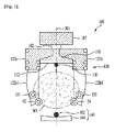
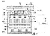
実施例はウエハー製造工程中にウエハーを移送する工程に使われることができる。
Claims (20)
- 垂直方向又は水平方向に移動するガイド(guide);
前記ガイドに取り付けられ、互いに離隔したウエハーを装着させる移送アーム;
前記ガイドに配置され、前記移送アームに装着された互いに離隔したウエハーに第1レーザーを放出するレーザー放出部;及び
前記移送アームの下側に配置され、前記第1レーザーのうち前記互いに離隔したウエハーの間の隙間を通過した第2レーザーを捕集するレーザー感知部を含む、ウエハー移送装置。 - 前記レーザー放出部から照射される第1レーザー、及びレーザー捕集器によって捕集される第2レーザーに基づき、前記互いに離隔したウエハーの厚さを測定する制御部をさらに含む、請求項1に記載のウエハー移送装置。
- 前記第1レーザーの水平方向の放出領域の一端は前記ウエハーのうち第1ウエハーのエッジに整列され、前記第1レーザーの水平方向の放出領域の他端は前記ウエハーのうち最後のウエハーのエッジに整列される、請求項1に記載のウエハー移送装置。
- 前記ガイドと前記レーザー感知部の間に連結され、前記レーザー感知部を前記ガイドに固定させるレーザー感知支持部をさらに含む、請求項1に記載のウエハー移送装置。
- 前記レーザー感知支持部は前記ガイドと一緒に水平方向又は垂直方向に移動する、請求項4に記載のウエハー移送装置。
- 前記レーザー感知支持部は、
前記ガイドの一端と前記レーザー感知部の一端を連結する第1レーザー感知支持部;及び
前記ガイドの他端と前記レーザー感知部の他端を連結する第2レーザー感知支持部を含む、請求項4に記載のウエハー移送装置。 - 前記移送アームは、
前記ガイドの一端に結合される第1及び第2アーム;
前記ガイドの他端に結合される第3及び第4アーム;
前記第1〜第4アームと連結される支持部;及び
前記支持部と連結され、前記ウエハーが載置される載置棒を含む、請求項1に記載のウエハー移送装置。 - 前記第1〜第4アームは前記ガイドに結合された部分を軸として回転移動する、請求項7に記載のウエハー移送装置。
- 前記載置棒は、
一端が前記第1支持部に連結され、他端が第3支持部に連結される第1及び第2載置棒;及び
一端が前記第2支持部に連結され、他端が第4支持部に連結される第3及び第4載置棒を含む、請求項7に記載のウエハー移送装置。 - 前記第1〜第4載置棒は前記ウエハーが装着されるスロット(slot)を含む、請求項9に記載のウエハー移送装置。
- 前記ガイドを水平方向に移動させる移送レールをさらに含む、請求項1に記載のウエハー移送装置。
- 前記ガイドは、
前記移送レールによって水平方向に移動し、前記移送アームと連結される水平ガイド;及び
前記水平ガイドと連結され、前記水平ガイドを垂直方向に移動させる垂直ガイドを含む、請求項11に記載のウエハー移送装置。 - 垂直方向又は水平方向に移動するガイド(guide);
前記ガイドと連結され、互いに離隔したウエハーを装着させる移送アーム;
前記ガイドに配置され、前記移送アームに装着された互いに離隔したウエハーにレーザーを放出するレーザー放出部;
前記移送アームの下側に配置され、前記互いに離隔したウエハーの間の隙間を通過したレーザーを捕集するレーザー感知部;及び
前記レーザー捕集器によって捕集されなかった領域の長さを算出し、算出された長さのそれぞれに対応するウエハーの厚さを測定する制御部を含む、ウエハー移送装置。 - レーザーを照射するレーザー放出部及びレーザーを感知するレーザー感知部を備えるウエハー移送装置に装着されたウエハーを加工するウエハー加工方法であって、
前記レーザー放出部によって、前記ウエハー移送装置に装着されたウエハーにレーザーを照射するレーザー照射段階;
前記レーザー感知部によって、前記ウエハー移送装置に装着されたウエハーの間を通過したレーザーを感知するレーザー感知段階;
前記感知された結果によって、前記ウエハー移送装置に装着されたウエハーの厚さを測定する厚さ測定段階;及び
前記測定された厚さに基づき、前記ウエハー移送装置に装着されたウエハーを加工する加工段階を含む、ウエハー加工方法。 - 前記ウエハー移送装置によって前記ウエハーを移送する段階をさらに含み、
前記レーザー照射段階、前記レーザー感知段階、及び前記厚さ測定段階は前記移送する段階中に行う、請求項14に記載のウエハー加工方法。 - 前記測定されたウエハーの厚さを既設定の厚さ値と比較する比較段階をさらに含み、
前記加工段階は、前記比較段階によって比較された結果によって前記ウエハーの加工進行を決定するかあるいは加工時間を制御する、請求項14に記載のウエハー加工方法。 - 前記加工段階は前記ウエハーを食刻する段階である、請求項14に記載のウエハー加工方法。
- 前記加工段階後、前記レーザー照射段階、前記レーザー感知段階、及び前記厚さ測定段階を行うことで、前記加工段階によって加工されたウエハーの厚さを測定する厚さ測定段階;及び
前記加工段階によって加工されたウエハーの測定された厚さが既設定の厚さと同じになるまで、前記レーザー照射段階、前記レーザー感知段階、前記厚さ測定段階、前記比較段階、及び前記加工段階を繰り返し行う段階をさらに含む、請求項16に記載のウエハー加工方法。 - 前記加工段階は、前記食刻段階で食刻されたウエハーを洗浄する洗浄段階をさらに含む、請求項17に記載のウエハー加工方法。
- 前記加工段階は、前記洗浄段階で洗浄されたウエハーを乾燥させる乾燥段階をさらに含む、請求項19に記載のウエハー加工方法。
Applications Claiming Priority (3)
| Application Number | Priority Date | Filing Date | Title |
|---|---|---|---|
| KR1020150010385A KR101680214B1 (ko) | 2015-01-22 | 2015-01-22 | 웨이퍼 이송 장치 |
| KR10-2015-0010385 | 2015-01-22 | ||
| PCT/KR2015/006131 WO2016117777A1 (ko) | 2015-01-22 | 2015-06-17 | 웨이퍼 이송 장치 |
Publications (2)
| Publication Number | Publication Date |
|---|---|
| JP2018509751A true JP2018509751A (ja) | 2018-04-05 |
| JP6486478B2 JP6486478B2 (ja) | 2019-03-20 |
Family
ID=56417288
Family Applications (1)
| Application Number | Title | Priority Date | Filing Date |
|---|---|---|---|
| JP2017536278A Active JP6486478B2 (ja) | 2015-01-22 | 2015-06-17 | ウエハー移送装置 |
Country Status (6)
| Country | Link |
|---|---|
| US (1) | US10192794B2 (ja) |
| JP (1) | JP6486478B2 (ja) |
| KR (1) | KR101680214B1 (ja) |
| CN (1) | CN107210255B (ja) |
| DE (1) | DE112015006031B4 (ja) |
| WO (1) | WO2016117777A1 (ja) |
Families Citing this family (3)
| Publication number | Priority date | Publication date | Assignee | Title |
|---|---|---|---|---|
| US11352698B2 (en) * | 2019-04-25 | 2022-06-07 | Samsung Electronics Co., Ltd. | Atomic layer deposition apparatus and methods of fabricating semiconductor devices using the same |
| KR102825817B1 (ko) | 2020-08-28 | 2025-06-30 | 삼성전자주식회사 | 두께 추정 방법 및 공정 제어 방법 |
| KR20240146358A (ko) * | 2023-03-29 | 2024-10-08 | 에스케이실트론 주식회사 | 웨이퍼 분리 장치 |
Citations (15)
| Publication number | Priority date | Publication date | Assignee | Title |
|---|---|---|---|---|
| JPH02198152A (ja) * | 1989-01-27 | 1990-08-06 | Hitachi Electron Eng Co Ltd | カセット内ウェハのハンドリング方法および装置 |
| JPH02106830U (ja) * | 1989-02-09 | 1990-08-24 | ||
| JPH03250749A (ja) * | 1990-02-28 | 1991-11-08 | Mitsubishi Electric Corp | 半導体ウエハ移替装置におけるウエハ検出装置および方法 |
| JPH05152423A (ja) * | 1991-08-30 | 1993-06-18 | Dainippon Screen Mfg Co Ltd | 表面処理装置 |
| JPH05315309A (ja) * | 1992-05-01 | 1993-11-26 | Kaijo Corp | 半導体基板自動処理装置 |
| JPH06151401A (ja) * | 1992-11-05 | 1994-05-31 | Tokyo Electron Ltd | 被処理体検出装置 |
| JPH0837229A (ja) * | 1994-07-25 | 1996-02-06 | Nippon Telegr & Teleph Corp <Ntt> | 基板ティーチング装置 |
| JPH0851092A (ja) * | 1994-08-08 | 1996-02-20 | Tokyo Electron Ltd | 処理装置及び洗浄装置 |
| JPH11176912A (ja) * | 1997-12-08 | 1999-07-02 | Mitsubishi Electric Corp | 半導体基板処理装置及びその制御方法 |
| JP2002064075A (ja) * | 2000-06-05 | 2002-02-28 | Tokyo Electron Ltd | 液処理装置および液処理方法 |
| US20030082840A1 (en) * | 2001-10-26 | 2003-05-01 | Larry Frisa | Method and system for determining a thickness of a layer |
| JP2008177329A (ja) * | 2007-01-18 | 2008-07-31 | Mitsubishi Electric Corp | ウエットエッチング方法 |
| US20090227047A1 (en) * | 2008-03-06 | 2009-09-10 | Taiwan Semiconductor Manufacturing Co., Ltd. | Method and apparatus for thinning a substrate |
| JP2013153141A (ja) * | 2011-12-27 | 2013-08-08 | Shibaura Mechatronics Corp | 基板の処理装置及び処理方法 |
| JP2014175608A (ja) * | 2013-03-12 | 2014-09-22 | Tokyo Electron Ltd | 基板搬送装置、基板処理装置、基板取出方法および記憶媒体 |
Family Cites Families (12)
| Publication number | Priority date | Publication date | Assignee | Title |
|---|---|---|---|---|
| JPH02106830A (ja) | 1988-10-17 | 1990-04-18 | Meidensha Corp | 真空インタラプタ用電極の製造方法 |
| US5319216A (en) | 1991-07-26 | 1994-06-07 | Tokyo Electron Limited | Substrate detector with light emitting and receiving elements arranged in staggered fashion and a polarization filter |
| KR0118207B1 (ko) | 1992-09-25 | 1997-09-30 | 기다오까 다까시 | 반도체 세정장치 및 웨이퍼카세트 |
| JP3110218B2 (ja) * | 1992-09-25 | 2000-11-20 | 三菱電機株式会社 | 半導体洗浄装置及び方法、ウエハカセット、専用グローブ並びにウエハ受け治具 |
| JPH08129353A (ja) | 1994-11-01 | 1996-05-21 | Casio Comput Co Ltd | 表示装置 |
| JP3422799B2 (ja) * | 1998-05-01 | 2003-06-30 | 東京エレクトロン株式会社 | 膜厚測定装置、基板処理方法並びに基板処理装置 |
| JP4389305B2 (ja) * | 1999-10-06 | 2009-12-24 | 東京エレクトロン株式会社 | 処理装置 |
| US8313277B2 (en) * | 2003-11-10 | 2012-11-20 | Brooks Automation, Inc. | Semiconductor manufacturing process modules |
| KR20060039134A (ko) | 2004-11-02 | 2006-05-08 | 삼성전자주식회사 | 웨이퍼 카세트 어라인 장치 |
| KR101339002B1 (ko) | 2006-12-13 | 2013-12-09 | (주)스마트에이스 | 기판식각장치 및 식각방법 |
| US8129279B2 (en) * | 2008-10-13 | 2012-03-06 | Taiwan Semiconductor Manufacturing Co., Ltd. | Chemical mechanical polish process control for improvement in within-wafer thickness uniformity |
| KR101469000B1 (ko) | 2013-07-17 | 2014-12-04 | 주식회사 엠엠테크 | 글라스 박형화 장치 및 그 방법 |
-
2015
- 2015-01-22 KR KR1020150010385A patent/KR101680214B1/ko active Active
- 2015-06-17 JP JP2017536278A patent/JP6486478B2/ja active Active
- 2015-06-17 CN CN201580074090.1A patent/CN107210255B/zh active Active
- 2015-06-17 US US15/541,631 patent/US10192794B2/en active Active
- 2015-06-17 WO PCT/KR2015/006131 patent/WO2016117777A1/ko not_active Ceased
- 2015-06-17 DE DE112015006031.6T patent/DE112015006031B4/de active Active
Patent Citations (15)
| Publication number | Priority date | Publication date | Assignee | Title |
|---|---|---|---|---|
| JPH02198152A (ja) * | 1989-01-27 | 1990-08-06 | Hitachi Electron Eng Co Ltd | カセット内ウェハのハンドリング方法および装置 |
| JPH02106830U (ja) * | 1989-02-09 | 1990-08-24 | ||
| JPH03250749A (ja) * | 1990-02-28 | 1991-11-08 | Mitsubishi Electric Corp | 半導体ウエハ移替装置におけるウエハ検出装置および方法 |
| JPH05152423A (ja) * | 1991-08-30 | 1993-06-18 | Dainippon Screen Mfg Co Ltd | 表面処理装置 |
| JPH05315309A (ja) * | 1992-05-01 | 1993-11-26 | Kaijo Corp | 半導体基板自動処理装置 |
| JPH06151401A (ja) * | 1992-11-05 | 1994-05-31 | Tokyo Electron Ltd | 被処理体検出装置 |
| JPH0837229A (ja) * | 1994-07-25 | 1996-02-06 | Nippon Telegr & Teleph Corp <Ntt> | 基板ティーチング装置 |
| JPH0851092A (ja) * | 1994-08-08 | 1996-02-20 | Tokyo Electron Ltd | 処理装置及び洗浄装置 |
| JPH11176912A (ja) * | 1997-12-08 | 1999-07-02 | Mitsubishi Electric Corp | 半導体基板処理装置及びその制御方法 |
| JP2002064075A (ja) * | 2000-06-05 | 2002-02-28 | Tokyo Electron Ltd | 液処理装置および液処理方法 |
| US20030082840A1 (en) * | 2001-10-26 | 2003-05-01 | Larry Frisa | Method and system for determining a thickness of a layer |
| JP2008177329A (ja) * | 2007-01-18 | 2008-07-31 | Mitsubishi Electric Corp | ウエットエッチング方法 |
| US20090227047A1 (en) * | 2008-03-06 | 2009-09-10 | Taiwan Semiconductor Manufacturing Co., Ltd. | Method and apparatus for thinning a substrate |
| JP2013153141A (ja) * | 2011-12-27 | 2013-08-08 | Shibaura Mechatronics Corp | 基板の処理装置及び処理方法 |
| JP2014175608A (ja) * | 2013-03-12 | 2014-09-22 | Tokyo Electron Ltd | 基板搬送装置、基板処理装置、基板取出方法および記憶媒体 |
Also Published As
| Publication number | Publication date |
|---|---|
| KR101680214B1 (ko) | 2016-11-28 |
| CN107210255B (zh) | 2020-05-05 |
| DE112015006031T5 (de) | 2017-09-28 |
| WO2016117777A1 (ko) | 2016-07-28 |
| US10192794B2 (en) | 2019-01-29 |
| DE112015006031B4 (de) | 2022-05-12 |
| CN107210255A (zh) | 2017-09-26 |
| US20180005907A1 (en) | 2018-01-04 |
| JP6486478B2 (ja) | 2019-03-20 |
| KR20160090515A (ko) | 2016-08-01 |
Similar Documents
| Publication | Publication Date | Title |
|---|---|---|
| TWI445651B (zh) | 感測器單元、器械、導軌系統、倉儲系統及管理倉儲之方法 | |
| US9960063B2 (en) | Substrate transport apparatus and substrate transport method | |
| JP5333158B2 (ja) | 液体試料配置機構、それを用いた屈折率測定装置及び屈折率測定方法 | |
| KR20160138293A (ko) | 반도체 웨이퍼 검사용 x-레이 검사 장치들 | |
| JP6486478B2 (ja) | ウエハー移送装置 | |
| US20080227228A1 (en) | Measurement of Overlay Offset in Semiconductor Processing | |
| KR102264851B1 (ko) | 포크 로봇 및 포크의 삽입 거리 산출 방법 | |
| JP4490779B2 (ja) | 基板処理装置 | |
| KR102013671B1 (ko) | 기판 처리 장치 및 처리액 노즐 검사 방법 | |
| CN108168444A (zh) | 用于pcb应用的在空气悬浮上的在线计量 | |
| KR20130114617A (ko) | 그래핀 기판 검사 장치 및 그 방법 | |
| JP6333065B2 (ja) | 塗布装置 | |
| TW201421594A (zh) | 用於檢查基板之靜電之設備及製造基板之方法 | |
| KR101469000B1 (ko) | 글라스 박형화 장치 및 그 방법 | |
| KR102405151B1 (ko) | 접액 노즐의 세정 방법 및 세정 장치 | |
| KR102852464B1 (ko) | 기판 처리 방법 및 기판 처리 장치 | |
| JP2013235915A (ja) | シート抵抗率計測機構付きレーザアニール装置 | |
| KR102740300B1 (ko) | 기판 처리 장치 및 기판 처리 방법 | |
| KR20110070265A (ko) | 레이저 빔 프로파일러를 구비하는 레이저 가공장치 | |
| KR101581372B1 (ko) | 노치리스 웨이퍼 제조 장치 및 이의 제조 방법 | |
| CN110361936A (zh) | 掩模版厚度检测装置、存储机构、传输机构及光刻系统 | |
| US9086352B2 (en) | Stage device and driving method thereof | |
| KR101736849B1 (ko) | 기판 중심 검출 방법, 기판 반송 방법, 반송 유닛 및 이를 포함하는 기판 처리 장치. | |
| JP2008151714A (ja) | 板状部材検査装置 | |
| JP6121732B2 (ja) | 基板検査装置および基板検査方法 |
Legal Events
| Date | Code | Title | Description |
|---|---|---|---|
| A521 | Request for written amendment filed |
Free format text: JAPANESE INTERMEDIATE CODE: A523 Effective date: 20170707 |
|
| A621 | Written request for application examination |
Free format text: JAPANESE INTERMEDIATE CODE: A621 Effective date: 20170707 |
|
| A977 | Report on retrieval |
Free format text: JAPANESE INTERMEDIATE CODE: A971007 Effective date: 20180827 |
|
| A131 | Notification of reasons for refusal |
Free format text: JAPANESE INTERMEDIATE CODE: A131 Effective date: 20180911 |
|
| A521 | Request for written amendment filed |
Free format text: JAPANESE INTERMEDIATE CODE: A523 Effective date: 20181211 |
|
| TRDD | Decision of grant or rejection written | ||
| A01 | Written decision to grant a patent or to grant a registration (utility model) |
Free format text: JAPANESE INTERMEDIATE CODE: A01 Effective date: 20190122 |
|
| A61 | First payment of annual fees (during grant procedure) |
Free format text: JAPANESE INTERMEDIATE CODE: A61 Effective date: 20190219 |
|
| R150 | Certificate of patent or registration of utility model |
Ref document number: 6486478 Country of ref document: JP Free format text: JAPANESE INTERMEDIATE CODE: R150 |
|
| R250 | Receipt of annual fees |
Free format text: JAPANESE INTERMEDIATE CODE: R250 |
|
| R250 | Receipt of annual fees |
Free format text: JAPANESE INTERMEDIATE CODE: R250 |
|
| R250 | Receipt of annual fees |
Free format text: JAPANESE INTERMEDIATE CODE: R250 |
|
| R250 | Receipt of annual fees |
Free format text: JAPANESE INTERMEDIATE CODE: R250 |
|
| R250 | Receipt of annual fees |
Free format text: JAPANESE INTERMEDIATE CODE: R250 |