JP2019088185A - Dc motor drive circuit, drive method, and electronic device using the same - Google Patents
Dc motor drive circuit, drive method, and electronic device using the same Download PDFInfo
- Publication number
- JP2019088185A JP2019088185A JP2018200011A JP2018200011A JP2019088185A JP 2019088185 A JP2019088185 A JP 2019088185A JP 2018200011 A JP2018200011 A JP 2018200011A JP 2018200011 A JP2018200011 A JP 2018200011A JP 2019088185 A JP2019088185 A JP 2019088185A
- Authority
- JP
- Japan
- Prior art keywords
- drive
- motor
- command value
- value
- drive circuit
- Prior art date
- Legal status (The legal status is an assumption and is not a legal conclusion. Google has not performed a legal analysis and makes no representation as to the accuracy of the status listed.)
- Granted
Links
- 238000000034 method Methods 0.000 title claims description 19
- 238000001514 detection method Methods 0.000 claims abstract description 58
- 238000013459 approach Methods 0.000 claims abstract description 16
- 230000007274 generation of a signal involved in cell-cell signaling Effects 0.000 claims description 22
- 230000008859 change Effects 0.000 claims description 17
- 230000007704 transition Effects 0.000 claims description 11
- 239000004065 semiconductor Substances 0.000 claims description 7
- 239000000758 substrate Substances 0.000 claims description 7
- 230000004044 response Effects 0.000 claims description 6
- 230000010354 integration Effects 0.000 claims description 3
- 238000010586 diagram Methods 0.000 description 32
- 230000006870 function Effects 0.000 description 17
- 230000004048 modification Effects 0.000 description 15
- 238000012986 modification Methods 0.000 description 15
- 239000000872 buffer Substances 0.000 description 5
- 230000008569 process Effects 0.000 description 4
- 239000003990 capacitor Substances 0.000 description 3
- 238000012545 processing Methods 0.000 description 3
- CHBBVOLNJBUVGQ-UHFFFAOYSA-N (2,4-dioxo-1h-pyrimidin-5-yl)methyl phosphono hydrogen phosphate Chemical compound OP(O)(=O)OP(O)(=O)OCC1=CNC(=O)NC1=O CHBBVOLNJBUVGQ-UHFFFAOYSA-N 0.000 description 2
- 101100464779 Saccharomyces cerevisiae (strain ATCC 204508 / S288c) CNA1 gene Proteins 0.000 description 2
- 239000000470 constituent Substances 0.000 description 2
- 230000007423 decrease Effects 0.000 description 2
- 238000003708 edge detection Methods 0.000 description 2
- 230000007246 mechanism Effects 0.000 description 2
- 230000009467 reduction Effects 0.000 description 2
- 230000006641 stabilisation Effects 0.000 description 2
- 238000011105 stabilization Methods 0.000 description 2
- 101100524516 Saccharomyces cerevisiae (strain ATCC 204508 / S288c) RFA2 gene Proteins 0.000 description 1
- 230000002159 abnormal effect Effects 0.000 description 1
- 230000005856 abnormality Effects 0.000 description 1
- 239000013256 coordination polymer Substances 0.000 description 1
- 230000003247 decreasing effect Effects 0.000 description 1
- 238000011161 development Methods 0.000 description 1
- 238000006073 displacement reaction Methods 0.000 description 1
- 230000014509 gene expression Effects 0.000 description 1
- 230000006698 induction Effects 0.000 description 1
- 230000002093 peripheral effect Effects 0.000 description 1
- 230000000630 rising effect Effects 0.000 description 1
- 230000002459 sustained effect Effects 0.000 description 1
Images


Landscapes
- Control Of Motors That Do Not Use Commutators (AREA)
Abstract
Description
本発明は、DCモータの駆動回路に関する。 The present invention relates to a drive circuit of a DC motor.
制御対象を位置決めするためにステッピングモータが用いられる。ステッピングモータの制御には、クロック信号(パルスレート信号)が用いられ、入力したクロック信号のパルス数に比例して、モータをオープンループで回転させることができ、またクロック信号を停止した状態では、モータを静止させることができる。こうした制御の容易性から、プリンタやファクシミリ、スキャナ、複合機などのOA機器、あるいは産業機器においては、ステッピングモータが多く用いられている。 A stepping motor is used to position the control target. A clock signal (pulse rate signal) is used to control the stepping motor, and the motor can be rotated in an open loop in proportion to the number of pulses of the input clock signal, and when the clock signal is stopped, The motor can be stationary. Because of such ease of control, stepping motors are often used in office automation equipment such as printers, facsimiles, scanners, multifunction machines, etc., or in industrial equipment.
ところが、ステッピングモータは、静止状態においても、コイルが通電し続けるため、消費電力が大きくなるという問題がある。近年、OA機器をはじめとするさまざまなアプリケーションにおいて、低消費電力化が求められているが、ステッピングモータの消費電力が、OA機器の低消費電力化を妨げる一因となっている。 However, the stepping motor has a problem that power consumption increases because the coil continues to be energized even in the stationary state. In recent years, low power consumption has been required in various applications including OA equipment, but the power consumption of a stepping motor is one factor that hinders the reduction in power consumption of the OA equipment.
ブラシレスDCモータは制御が複雑であるが、消費電力が小さいという特徴を有する。したがって今後、低消費電力化が求められるアプリケーションでは、ステッピングモータをDCモータに置換していくことが求められる。 The brushless DC motor is characterized in that control is complicated but power consumption is small. Therefore, from now on, in applications where low power consumption is required, it is required to replace the stepping motor with a DC motor.
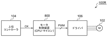
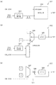
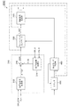
図1は、DCモータを備えるモータ駆動システムのブロック図である。このモータ駆動システムでは、従来のステッピングモータと同様に、クロック信号を利用した制御インタフェースで、DCモータを制御する。モータ駆動システム100Rは、DCモータ102、上位コントローラ104、ドライバ106およびモータ制御装置800を備える。上位コントローラ104は、たとえばマイコンやCPU(Central Processing Unit)であり、DCモータ102のロータの位置を指示するクロック信号CKを生成する。モータ制御装置800もまたCPUやマイコンで構成され、ソフトウェア制御によって、クロック信号をDCモータの駆動に適合したPWM信号に変換する。ドライバ106は、三相インバータを含み、PWM信号にもとづいてDCモータ102を駆動する。このようなシステムは、たとえば特許文献1に記載される。
FIG. 1 is a block diagram of a motor drive system provided with a DC motor. In this motor drive system, the DC motor is controlled by a control interface using a clock signal as in the case of a conventional stepping motor. The
課題1.
CPUやマイコンは高価であるため、DCモータの制御のためのモータ制御装置800をCPUやマイコンで構成すると、機器のコストが高くなるという問題がある。
Since the CPU and the microcomputer are expensive, if the
また、モータ駆動システム100Rの設計者は、クロック信号CKの仕様、駆動対象のDCモータ102の特性等を考慮して、モータ制御装置800が実行するソフトウェアプログラムを作成する必要があり、開発コストの高騰、開発期間の長期化という問題を引き起こす。
In addition, the designer of the
課題2.
多くのアプリケーションにおいて、ステッピングモータを回転動作させる期間と、回転停止させる期間(保持動作)が交互に発生する。外力がない状況では、DCモータへの給電を停止することでDCモータを静止することが可能であるが、外力が加わる状況では、DCモータに外力と釣り合うトルクを発生させる必要がある。
In many applications, a period for rotating the stepping motor and a period for stopping the rotation (holding operation) occur alternately. In the situation where there is no external force, it is possible to stop the DC motor by stopping the power supply to the DC motor, but in the situation where the external force is applied, it is necessary to generate a torque that balances the external force with the external force.
本発明のある態様は、課題1および/または2を解決することが可能な駆動回路の提供にある。
An embodiment of the present invention is to provide a drive circuit capable of solving the
1. 本発明のある態様は、DCモータの駆動回路に関する。駆動回路は、ロジック回路で構成され、上位コントローラからのクロック信号と、エンコーダからのパルス信号と、を受け、パルス信号にもとづくロータの現在位置と、クロック信号にもとづくロータの目標位置との差分である位置誤差値を生成する誤差検出器と、ロジック回路で構成され、位置誤差値がゼロに近づくように指令値を生成するフィードバックコントローラと、ロジック回路で構成され、指令値に応じた駆動信号を生成する駆動信号生成部と、を備え、ひとつの半導体基板に集積化される。 1. One embodiment of the present invention relates to a drive circuit of a DC motor. The drive circuit is composed of a logic circuit, receives the clock signal from the host controller and the pulse signal from the encoder, and is the difference between the current position of the rotor based on the pulse signal and the target position of the rotor based on the clock signal. An error detector that generates a position error value, a feedback controller that generates a command value such that the position error value approaches zero, and a logic circuit that is configured by a logic circuit, and a drive signal that corresponds to the command value And a drive signal generation unit to be generated, and integrated on one semiconductor substrate.
2. 本発明のある態様はDCモータの駆動回路に関する。駆動回路は、上位コントローラからのクロック信号と、エンコーダからのパルス信号と、に応じてDCモータを駆動する。駆動回路は、クロック信号にもとづくロータの目標位置を示す位置指令値と、パルス信号にもとづくロータの現在位置を示す位置検出値との差分に応じた位置誤差値を生成する誤差検出器と、位置誤差値がゼロに近づくようにトルク指令値を生成するフィードバックコントローラと、トルク指令値に応じた駆動信号を生成する駆動信号生成部と、を備える。駆動回路は、回転制御モードと保持モードが切りかえ可能であり、回転制御モードと保持モードでフィードバックコントローラの制御特性が切り替わる。 2. One embodiment of the present invention relates to a drive circuit of a DC motor. The drive circuit drives the DC motor according to the clock signal from the host controller and the pulse signal from the encoder. An error detector that generates a position error value according to a difference between a position command value indicating a target position of the rotor based on the clock signal and a position detection value indicating the current position of the rotor based on the pulse signal; A feedback controller that generates a torque command value so that the error value approaches zero, and a drive signal generation unit that generates a drive signal according to the torque command value. The drive circuit can switch between the rotation control mode and the holding mode, and the control characteristic of the feedback controller is switched between the rotation control mode and the holding mode.
なお、以上の構成要素の任意の組み合わせや本発明の構成要素や表現を、方法、装置、システムなどの間で相互に置換したものもまた、本発明の態様として有効である。 It is to be noted that any combination of the above-described constituent elements, or one in which the constituent elements and expressions of the present invention are mutually replaced among methods, apparatuses, systems, etc. is also effective as an aspect of the present invention.
本発明のある態様によれば、安価にステッピングモータをDCモータに置換できる。また別の態様によれば、回転動作時の応答性を損なわずに、DCモータを停止させることができる。 According to an aspect of the present invention, the stepping motor can be replaced with a DC motor inexpensively. According to another aspect, it is possible to stop the DC motor without impairing the response during the rotation operation.
(実施の形態の概要1)
本明細書に開示される一実施の形態は、モータ駆動回路(駆動IC)に関する。モータ駆動ICは、ロジック回路で構成され、上位コントローラからのクロック信号と、エンコーダからのパルス信号と、を受け、パルス信号にもとづくロータの現在位置と、クロック信号にもとづくロータの目標位置との差分である位置誤差値を生成する誤差検出器と、ロジック回路で構成され、位置誤差値がゼロに近づくように指令値を生成するフィードバックコントローラと、ロジック回路で構成され、指令値に応じた駆動信号を生成する駆動信号生成部と、を備え、ひとつの半導体基板に集積化される。
(Summary of Embodiment 1)
One embodiment disclosed herein relates to a motor drive circuit (drive IC). The motor drive IC comprises a logic circuit, receives a clock signal from the host controller and a pulse signal from the encoder, and a difference between the current position of the rotor based on the pulse signal and the target position of the rotor based on the clock signal. An error detector that generates a position error value, and a feedback controller that is configured with a logic circuit and that generates a command value such that the position error value approaches zero, and a drive signal according to the command value And a drive signal generation unit for generating the signal, which is integrated on one semiconductor substrate.
この駆動ICを用いることにより、マイコンやCPU等が不要となり、ステッピングモータを安価にDCモータに置き換えることができ、システムの消費電力を低減できる。 By using this drive IC, a microcomputer, a CPU, etc. become unnecessary, the stepping motor can be replaced with a DC motor at low cost, and the power consumption of the system can be reduced.
フィードバックコントローラは、PI(比例積分)制御器を含んでもよい。PI制御器の制御特性は、クロック信号の周波数に応じて動的に変化してもよい。これにより、追従性を高めることができる。 The feedback controller may include a PI (proportional integration) controller. The control characteristics of the PI controller may change dynamically according to the frequency of the clock signal. Thereby, followability can be improved.
PI制御器の積分ゲインは一定であり、比例ゲインがクロック信号の周波数に応じて変化してもよい。積分ゲインを一定とすることにより、回転数の振動を抑制できる。 The integral gain of the PI controller is constant, and the proportional gain may change according to the frequency of the clock signal. By making the integral gain constant, vibration of the rotational speed can be suppressed.
誤差検出器は、クロック信号のエッジの個数の積算値に応じたターゲット値を生成する位置指令値生成部と、パルス信号にもとづき、ロータの現在位置を示すフィードバック値を生成する位置検出値生成部と、ターゲット値とフィードバック値の差分を生成する減算器と、を含んでもよい。 The error detector generates a target value according to an integrated value of the number of edges of the clock signal, and a position detection value generator that generates a feedback value indicating the current position of the rotor based on the pulse signal. And a subtractor that generates a difference between the target value and the feedback value.
位置指令値生成部は、クロック信号の1エッジあたりのターゲット値の変化量が複数値から選択可能であってもよい。これにより電子ギアを実現できる。 The position command value generation unit may be capable of selecting the amount of change of the target value per edge of the clock signal from a plurality of values. Thereby, an electronic gear can be realized.
位置検出値生成部は、パルス信号の1個あたりのフィードバック値の変化量が複数値から選択可能であってもよい。これにより電子ギアを実現できる。 The position detection value generation unit may be capable of selecting the amount of change in feedback value per pulse signal from a plurality of values. Thereby, an electronic gear can be realized.
駆動ICは、ターゲット値あるいはフィードバック値の変化量を指定するための設定ピンをさらに備えてもよい。 The drive IC may further include a setting pin for specifying the amount of change in the target value or the feedback value.
駆動ICは、DCモータを駆動するインバータを制御するプリドライバをさらに備えてもよい。 The drive IC may further include a predriver that controls an inverter that drives the DC motor.
(実施の形態の概要2)
本明細書に開示される一実施の形態は、モータ駆動回路に関する。モータ駆動回路は、上位コントローラからのクロック信号と、エンコーダからのパルス信号と、に応じてDCモータを駆動する。
駆動回路は、クロック信号にもとづくロータの目標位置を示す位置指令値と、パルス信号にもとづくロータの現在位置を示す位置検出値との差分に応じた位置誤差値を生成する誤差検出器と、位置誤差値がゼロに近づくようにトルク指令値を生成するフィードバックコントローラと、トルク指令値に応じた駆動信号を生成する駆動信号生成部と、を備える。駆動回路は、回転制御モードと保持モードが切りかえ可能であり、回転制御モードと保持モードでフィードバックコントローラの制御特性(制御パラメータ)が切り替わる。
(Summary of Embodiment 2)
One embodiment disclosed herein relates to a motor drive circuit. The motor drive circuit drives the DC motor according to the clock signal from the host controller and the pulse signal from the encoder.
An error detector that generates a position error value according to a difference between a position command value indicating a target position of the rotor based on the clock signal and a position detection value indicating the current position of the rotor based on the pulse signal; A feedback controller that generates a torque command value so that the error value approaches zero, and a drive signal generation unit that generates a drive signal according to the torque command value. The drive circuit can switch between the rotation control mode and the holding mode, and the control characteristic (control parameter) of the feedback controller is switched between the rotation control mode and the holding mode.
回転制御モードではクロック信号にもとづく回転指令に対する追従性を重視した制御パラメータを与え、保持モードでは、追従性ではなく、安定性を重視した制御パラメータを与えることで、DCモータをステッピングモータのように駆動することが可能となる。 In the rotation control mode, a control parameter that emphasizes the followability to the rotation command based on the clock signal is given, and in the hold mode, a control parameter that emphasizes stability, not the followability, gives the DC motor like a stepping motor. It becomes possible to drive.
フィードバックコントローラはPI(Proportional Integral)制御器を含んでもよい。回転制御モードと保持モードとで、比例ゲインと積分ゲインの少なくとも一方が異なってもよい。 The feedback controller may include a PI (Proportional Integral) controller. At least one of the proportional gain and the integral gain may be different between the rotation control mode and the holding mode.
積分値が残留した状態でモードが切り替わると、積分値がゼロになるまでトルクが発生し続け、不要な振動を引き起こしたり、制御が安定するまでの遅延が長くなる可能性がある。そこで回転制御モードと保持モードが切り替わる際に、積分値がゼロリセットすることにより、不要な振動を抑制し、あるいは安定時間を短縮できる。 If the mode is switched while the integral value remains, torque may continue to be generated until the integral value becomes zero, which may cause unnecessary vibration or a long delay until the control is stabilized. Therefore, when the rotation control mode and the holding mode are switched, by resetting the integral value to zero, unnecessary vibration can be suppressed or the stabilization time can be shortened.
駆動回路は、クロック信号の入力状態にもとづいて、回転制御モードと保持モードを判定するモード判定部をさらに備えてもよい。クロック信号の無入力状態はモータの停止指示であるから、追加の制御線を必要とせずに、回転制御モードと保持モードを切り替えることができる。 The drive circuit may further include a mode determination unit that determines the rotation control mode and the holding mode based on the input state of the clock signal. Since the non-input state of the clock signal is a motor stop instruction, the rotation control mode and the holding mode can be switched without requiring an additional control line.
モード判定部は、クロック信号の無入力状態の持続時間を測定するカウンタを含み、クロック信号の無入力状態が所定時間持続すると、回転制御モードから保持モードに移行してもよい。 The mode determination unit may include a counter that measures the duration of the non-input state of the clock signal, and may shift from the rotation control mode to the hold mode when the non-input state of the clock signal continues for a predetermined time.
フィードバックコントローラは、回転制御モードに関連する第1コントローラと、保持モードに関連する第2コントローラと、を含んでもよい。コントローラを2系統用意することにより、シームレスな切り替えが可能となる。 The feedback controller may include a first controller associated with the rotational control mode and a second controller associated with the hold mode. By preparing two systems of controllers, seamless switching becomes possible.
フィードバックコントローラは、単一のコントローラを含み、回転制御モードと保持モードとで、ゲインが変更されてもよい。 The feedback controller includes a single controller, and the gain may be changed in the rotation control mode and the hold mode.
駆動信号生成部は、トルク指令値に応じたデューティ比を有するPWM(Pulse Width Modulation)信号を生成するパルス幅変調器と、PWM信号とホールコンパレータの出力とにもとづいて駆動信号を生成する通電ロジックと、を含んでもよい。 The drive signal generation unit generates a drive signal based on the pulse width modulator that generates a PWM (Pulse Width Modulation) signal having a duty ratio corresponding to the torque command value, and the PWM signal and the output of the hall comparator. And may be included.
駆動回路はDCモータを駆動するインバータを制御するプリドライバをさらに備えてもよい。 The drive circuit may further include a predriver that controls an inverter that drives the DC motor.
駆動回路は、ひとつの半導体基板に一体集積化されてもよい。「一体集積化」とは、回路の構成要素のすべてが半導体基板上に形成される場合や、回路の主要構成要素が一体集積化される場合が含まれ、回路定数の調節用に一部の抵抗やキャパシタなどが半導体基板の外部に設けられていてもよい。回路を1つのチップ上に集積化することにより、回路面積を削減することができるとともに、回路素子の特性を均一に保つことができる。 The drive circuit may be integrated on one semiconductor substrate. "Integrated integration" includes the case where all of the circuit components are formed on a semiconductor substrate, and the case where the main components of the circuit are integrally integrated. A resistor, a capacitor or the like may be provided outside the semiconductor substrate. By integrating the circuit on one chip, the circuit area can be reduced and the characteristics of the circuit elements can be kept uniform.
(実施の形態)
以下、本発明を好適な実施の形態をもとに図面を参照しながら説明する。各図面に示される同一または同等の構成要素、部材、処理には、同一の符号を付するものとし、適宜重複した説明は省略する。また、実施の形態は、発明を限定するものではなく例示であって、実施の形態に記述されるすべての特徴やその組み合わせは、必ずしも発明の本質的なものであるとは限らない。
Embodiment
Hereinafter, the present invention will be described based on preferred embodiments with reference to the drawings. The same or equivalent components, members, and processes shown in the drawings are denoted by the same reference numerals, and duplicating descriptions will be omitted as appropriate. In addition, the embodiments do not limit the invention and are merely examples, and all the features and combinations thereof described in the embodiments are not necessarily essential to the invention.
本明細書において、「部材Aが、部材Bと接続された状態」とは、部材Aと部材Bが物理的に直接的に接続される場合や、部材Aと部材Bが、電気的な接続状態に影響を及ぼさず、あるいは機能を阻害しない他の部材を介して間接的に接続される場合も含む。 In the present specification, "a state in which the member A is connected to the member B" means that the members A and B are physically directly connected, or the members A and B are electrically connected. It also includes the case of being indirectly connected through other members that do not affect the state or inhibit the function.
同様に、「部材Cが、部材Aと部材Bの間に設けられた状態」とは、部材Aと部材C、あるいは部材Bと部材Cが直接的に接続される場合のほか、電気的な接続状態に影響を及ぼさず、あるいは機能を阻害しない他の部材を介して間接的に接続される場合も含む。 Similarly, "a state in which the member C is provided between the member A and the member B" means that the member A and the member C, or the member B and the member C are directly connected, or the electric member It also includes the case of being indirectly connected through other members that do not affect the connection state or inhibit the function.
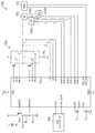
図2は、実施の形態に係る駆動IC200を備えるモータ駆動システム100のブロック図である。モータ駆動システム100は、駆動IC200に加えて、DCモータ102、上位コントローラ104、ドライバ106、ホールセンサ110U〜110W、エンコーダ112を備える。各信号の名称と、それが入出力されるピン(端子)、配線には同じ符号を付す。本実施の形態において駆動対象は三相DCモータである。
FIG. 2 is a block diagram of a
上位コントローラ104はマイコンやCPU、ASIC(Application Specified IC)、FPGA(Field Programmable Gate Array)などであり、DCモータ102のロータの目標位置(以下、単にモータの位置ともいう)を示すクロック信号CLKを生成する。また上位コントローラ104は、モータの回転方向を指示する方向指示信号(CW_CCW信号)を生成する。これらの信号は、駆動IC200の対応するピンCLK,CW_CCに入力される。たとえばCW_CCW信号のローは第1方向(たとえば時計回り)の回転指示であり、ハイは第2方向の回転指示(たとえば反時計回り)である。
The
ドライバ106は三相インバータおよびシャント抵抗RSを含む。三相インバータの各相の出力電圧VU〜VWは、駆動IC200のフィードバックピン(U〜W)に入力される。シャント抵抗RSは、三相インバータに流れる電流の経路上に設けられ、電流に比例した電圧降下(検出電圧)が発生する。シャント抵抗RSの電圧降下(電流検出信号)VCLは、駆動IC200のRCL(過電流検出電圧入力)ピンに入力される。電流検出信号VCLは、たとえばパルスバイパルスの電流制限(Current Limit)に用いることができる。
The
ホールセンサ110U〜110Wは、ロータの位置に応じた三相のホール信号HUP,HUN,HVP,HVN,HWP,HWNを生成する。これらの信号は、駆動IC200の対応するピンに入力される。
The
ホールセンサ110U〜110Wには、駆動IC200および外付けのトランジスタQ1や抵抗R11,R12によって生成されるホールバイアス信号VHBが供給される。
The
エンコーダ112は、ロータの位置に関する情報(絶対位置、相対位置もしくは変位量)を示すパルス信号(A相パルス信号EN_AとB相パルス信号EN_B)を生成する。これらのパルス信号は、駆動IC200の対応するピンに入力される。
The
駆動IC200は、CLK信号、CW_CCW信号、ホール信号HUP〜HWN、パルス信号EN_A,EN_Bにもとづいて、ドライバ106を制御するためのゲート信号を生成し、UH,VH,WH,UL,VL,WLピンから出力する。
The
ドライバ106のハイサイドトランジスタはNチャンネルであり、ゲート駆動のために、電源電圧VCCより高い電圧が必要である。駆動IC200はチャージポンプを内蔵しており、CP1,CP2およびVGピンには、外付けのキャパシタが接続される。
The high side transistor of the
駆動IC200は、ハードウェア、すなわちロジック回路やアナログ回路の組み合わせで構成される。本明細書における「ロジック回路で構成される」とはCPUやマイコンなどのようにソフトウェア制御が不要なアーキテクチャであることを意味する。
The
また駆動IC200の電源(VCC)ピンには電源電圧が供給され、接地(GND)ピンは接地される。
The power supply (VCC) pin of the
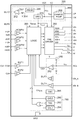
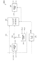
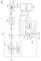
図3は、駆動IC200の構成を示すブロック図である。駆動IC200は、複数の入力バッファBUF1〜BUF4、ホールコンパレータHCMPU〜HCMPW、ロジック回路300、プリドライバ250、電源回路群260、保護回路280を備える。
FIG. 3 is a block diagram showing the configuration of the
複数の入力バッファBUFはそれぞれ、対応するピンに入力される信号をハイ、ロー2値化する。U相のホールコンパレータHCMPUは、HUPピンとHUNピンに入力される同じU相のホール信号HUP,HUNを比較する。V相、W相のホールコンパレータHHCMPV,HCMPWも同様である。入力バッファBUFおよびホールコンパレータHCMPの出力は、ロジック回路300に入力される。
The plurality of input buffers BUF high and low binarize signals input to the corresponding pins, respectively. The U-phase Hall comparator HCMPU compares the same U-phase Hall signals HUP and HUN input to the HUP pin and the HUN pin. The same applies to the Hall comparators HHCMPV and HCMPW of the V phase and the W phase. The outputs of the input buffer BUF and the Hall comparator HCMP are input to the
電源回路群260は、外付けの部品(図2のトランジスタQ11、抵抗R11,R12)とともにホールバイアス回路を構成するオペアンプ262、基準電圧源264を含む。ホールバイアス電圧VHBは、以下の電圧レベルに安定化される。
VHB=VREF×(1+R11/R12)
The power
V HB = V REF × (1 + R 11 / R 12 )
チャージポンプ266は、CPピン、CNピン、VGピンを介して外付けのキャパシタ(図2のC11,C12)接続される。チャージポンプ266には入力電圧として、電源電圧VCCが供給される。チャージポンプ266は、電源電圧VCCを昇圧し、VGピンに昇圧された高電圧VGを生成する。高電圧VGは、プリドライバ250に供給され、後段のハイサイドのトランジスタ(図2のドライバ106の上側アーム)の駆動に用いられる。
The
電源回路268はデジタル回路用の電源電圧VREGD(たとえば1.5V)を生成し、ロジック回路300に供給する。電源回路270はアナログ回路用の電源電圧VREG(たとえば5V)を生成し、ロジック回路300およびプリドライバ250に供給する。
The
保護回路280は、さまざまな保護回路を含む。TSD(Thermal Shut Down)回路282は、過熱状態を検出する。UVLO(Under Voltage Lock Out)回路284は、電源電圧VCCの低い状態を検出する。OVLO(Over Voltage Lock Out)回路286は、電源電圧VCCの過電圧状態を検出する。各回路の出力(検出信号)は、直接的に、あるいはORゲートを介して間接的に、ロジック回路300に入力される。
オシレータ288は、システムクロックCKSYSを生成し、ロジック回路300に供給する。
The
過電流検出回路290は、RCLピンに入力される検出電圧VCLにもとづく過電流保護のために設けられる。OCP(Over Current Protection)コンパレータ292は、検出電圧VCLをしきい値VTHと比較し、VCL>VTHとなると、OCP信号をアサート(たとえばハイ)する。OCP信号は、ロジック回路300に供給される。
The
ロジック回路300は、ホールコンパレータHCMPや入力バッファBUFの出力にもとづいて、駆動IC200の後段に接続されるドライバ(三相インバータ)106の駆動信号を生成する。また、各異常状態における保護処理を実行する。たとえばOCP信号がアサートされると、パルスバイパルスの過電流保護をかける。保護回路280において異常が検出されると、モータの駆動を停止する。
The
プリドライバ250は、ロジック回路300からの駆動信号およびU,V,Wピンにフィードバックされる各相のコイル端電圧VU,VV,VWにもとづいて、後段のドライバ106を駆動する。コイル端電圧VU,VV,VWは、ドライバ106のハイサイドトランジスタのゲート信号のローレベルの生成に使用される。
The pre-driver 250 drives the
以上が駆動IC200のブロック図である。続いて、ロジック回路300の構成を説明する。
The above is a block diagram of the
図4は、ロジック回路300の基本構成を示すブロック図である。ロジック回路300は、主として、誤差検出器310、フィードバックコントローラ330、駆動信号生成部340を備える。
FIG. 4 is a block diagram showing a basic configuration of
誤差検出器310は、エンコーダからのパルス信号EN_A,EN_Bと、上位コントローラからのクロック信号CKのパルス数の積算値との差分にもとづいて、ロータの目標位置と現在位置の誤差を示す位置誤差値ERRを生成する。
The
誤差検出器310は、位置指令値生成部312、位置検出値生成部314、減算器316を含む。位置指令値生成部312は、クロック信号CLKおよびCW_CCW信号にもとづいて、ロータの目標位置を示すターゲット値TGTを生成する。より詳しくは、位置指令値生成部312は、クロック信号CLKのポジエッジ(および/またはネガエッジ、以下、単にエッジという)の個数の積算値を生成する。
The
位置検出値生成部314は、エンコーダ112からのパルス信号EN_A,EN_Bにもとづいて、ロータの現在位置を示すフィードバック値FBを生成する。減算器316は、ターゲット値TGTとフィードバック値FBの差分を生成する。
The position detection
フィードバックコントローラ330は、位置誤差値ERRの値がゼロに近づくように、制御指令値REFを生成する。たとえばフィードバックコントローラ330は、PI(Proportional Integral)制御器を含むことができる。制御指令値REFは、モータのトルク指令値であってもよい。
The
駆動信号生成部340は、指令値REFに応じた駆動信号SUH,SUL,SVH,SVL,SWH,SWLを生成する。たとえば駆動信号生成部340は、パルス幅変調器342と、通電ロジック344を含む。パルス幅変調器342は、制御指令値REFに応じたデューティ比を有するPWM(Pulse Width Modulation)信号を生成する。
The drive
通電ロジック344は、CW_CCW信号にもとづいて回転方向を決定する。また通電ロジック344は、ホールコンパレータHCMPU〜HCMPWにもとづいて、駆動対象の相(駆動相)を切りかえる(転流制御)。通電方式は特に限定されないが、たとえば120度通電制御(矩形波駆動)を採用することができる。そのほか、180度通電制御(正弦波駆動)などの別の方式を採用してもよい。
The
通電ロジック344はPWM信号に応じて、駆動信号SUH,SUL,SVH,SVL,SWH,SWLのいずれかを変調する。PWM制御の方式は限定されないが、たとえばローサイ側の駆動信号SUL,SVL,SWLの論理を固定し、ハイサイドの駆動信号SUH,SVH,SWHの論理をPWM信号にもとづいて変調してもよい。反対に、ローサイドの駆動信号を変調してもよいし、両方を変調してもよい。
The
通電ロジック344は、OCP信号にもとづいて、パルスバイパルスの電流制限をかけてもよい。具体的には、OCP信号がアサートされると、通電中のトランジスタがターンオフするように駆動信号SUH〜SWH,SUL〜SWLを変化させる。
パルス幅変調器342、通電ロジック344の構成は、従来のDCモータの駆動回路のそれらと同様でよく、公知技術を用いればよい。
The configurations of the
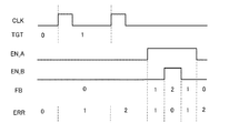
図5は、誤差検出器310の動作を説明する図である。この例では、CW_CCW信号をローとしている。クロック信号CLKのエッジが発生する度に、ターゲット値TGTが1増加し、その結果、位置誤差値ERRは1増加する。また、パルス信号EN_AとEN_Bの組み合わせによってフィードバック値FBが変化し、その結果、位置誤差値ERRが減少または増加する。
FIG. 5 is a diagram for explaining the operation of the
図6(a)〜(c)は、位置指令値生成部312の構成例を示すブロック図である。図6(a)の位置指令値生成部312は、クロック信号CLKのエッジを検出するエッジ検出回路320、エッジごとにカウントアップ/カウントダウンするカウンタ322を含む。回転方向を指示するCW_CCW信号は、カウンタ322のカウントアップ、カウントダウンの選択に用いられる。カウンタ322の出力が、ターゲット値TGTとなる。
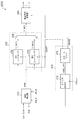
FIGS. 6A to 6C are block diagrams showing configuration examples of the position command
図6(b)の位置指令値生成部312は、演算器324、メモリ(レジスタ)325、オペコードセレクタ326を含む。演算器324は、少なくとも加算演算A+Bと、減算演算A−Bが、オペコード(OPECODE)に応じて切りかえ可能である。入力Aには、メモリ325の値(位置誤差値ERR)が入力され、入力Bには固定値1が入力される。オペコードセレクタ326は、クロック信号CLKのエッジが検出されるたびに、オペコードを発行する。オペコードは、CW_CCWが第1レベルのときに加算、CW_CCW信号が第2レベルのときに減算となる。これによりメモリ325には、クロック信号CLKのエッジの個数を積算した値が格納され、これはターゲット値TGTを表す。
The position command
図6(c)の位置指令値生成部312は、セレクタ327、加算器328、メモリ329を含む。セレクタ327には、値1と−1が入力されており、CW_CCWの値に応じた一方を選択する。加算器328はクロック信号CLKのエッジに応じて動作し、セレクタ327の出力と、メモリ329の値を加算し、加算結果によりメモリ329の値を更新する。これによりメモリ329には、クロック信号CLKのエッジの個数を積算した値が格納され、これはターゲット値TGTを表す。
The position command
以上がロジック回路300の構成である。
The above is the configuration of the
実施の形態に係る駆動IC200を用いることにより、従来のシステムにおけるマイコンやCPU(図1の900)が不要となるため、ステッピングモータを安価にDCモータに置き換えることができ、システムの消費電力を低減という利点を享受できる。
By using the
続いて、駆動IC200のさらなる特徴を説明する。
Subsequently, further features of the
(回転制御モードと保持モード)
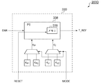
図7は、回転制御モードと保持モードの切り替えをサポートする駆動IC200Dのブロック図である。
(Rotation control mode and holding mode)
FIG. 7 is a block diagram of a
駆動IC200Dは、誤差検出器310、フィードバックコントローラ330、駆動信号生成部340に加えて、モード判定部470を備える。誤差検出器310、フィードバックコントローラ330、駆動信号生成部340の基本的な機能、動作については、図4を参照してすでに説明した。
The
誤差検出器310は、位置指令値生成部312、位置検出値生成部314、減算器316を含む。位置指令値生成部312は、クロック信号CLKにもとづき、ロータの目標位置を示す位置指令値P_TGTを生成する。位置指令値P_TGTは、図4における位置指令値TGTに相当する。
The
位置検出値生成部314は、エンコーダからのパルス信号EN_A,EN_Bにもとづき、ロータの現在位置を示す位置検出値P_FBを生成する。位置検出値P_FBは、図4のフィードバック値FBに相当する。
The position detection
位置指令値P_TGTおよび位置検出値P_FBは、減算器316に入力され、位置誤差値ERRが生成される。
Position command value P_TGT and position detection value P_FB are input to
フィードバックコントローラ330は、位置検出値P_FBが位置指令値P_TGTに近づくように、すなわち位置誤差値ERRがゼロに近づくように、トルク指令値T_REFを生成する。トルク指令値T_REFは、図4における指令値REFに相当する。トルク指令値T_REFは、駆動信号生成部340に供給される。
The
駆動IC200Dは、回転制御モードと保持モードが切りかえ可能に構成される。フィードバックコントローラ330の制御特性は、回転制御モードと保持モードで異なる。
The
上述のように、フィードバックコントローラ330はPI(Proportional Integral)制御器を含むことができる。回転制御モードと保持モードでは、比例ゲインKPと積分ゲインKIの少なくとも一方、好ましくは両方が異なる。
As mentioned above, the
典型的には、保持モードにおける比例ゲインKPは、回転制御モードにおける比例ゲインKPと等しいか、それより小さい。また保持モードにおける積分ゲインKIは、回転制御モードにおける積分ゲインKIと等しいか、それより小さい。 Typically, the proportional gain K P in hold mode is equal to or less than the proportional gain K P in rotational control mode. The integral gain K I in the holding mode, or equal to the integral gain K I in the rotation control mode is smaller than that.
モード判定部470は、クロック信号CKの入力状態にもとづいて、回転制御モードと保持モードを判定する。モード判定部470は、クロック信号CLKの無入力状態が所定時間持続すると、回転制御モードから保持モードに移行する。また、保持モードにおいてクロック信号CLKのエッジを検出すると、直ちに回転制御モードに移行する。
以上が駆動IC200Dの基本構成である。駆動IC200Dによれば、回転制御モードでは、クロック信号CLKにもとづく回転指令に対する追従性を重視した制御パラメータを与え、保持モードでは、追従性ではなく、安定性を重視した制御パラメータを与えることで、DCモータをステッピングモータのように駆動することが可能となる。
The above is the basic configuration of the
回転制御モードと保持モードが切り替わる際には、PIコントローラにおける積分値をゼロリセットすることが好ましい。これにより制御パラメータ切りかえにともなう不要振動の誘起、安定化時間の長期化を抑制できる。 When the rotation control mode and the holding mode are switched, it is preferable to reset the integrated value in the PI controller to zero. As a result, it is possible to suppress the induction of unnecessary vibration accompanying the switching of control parameters and the prolongation of the stabilization time.
さらに回転制御モードと保持モードとで、駆動信号生成部340(通電ロジック344)の動作、すなわち駆動信号の生成方法が異なっていてもよい。 Furthermore, the operation of the drive signal generator 340 (energization logic 344), that is, the method of generating the drive signal may be different between the rotation control mode and the holding mode.
たとえば駆動信号生成部340は、回転制御モードにおいては、CW_CCW信号に応じて回転方向を決定し、トルク指令値T_REFが正である場合に、トルク指令値T_REFに応じたデューティ比で、DCモータをPWM駆動する。トルク指令値T_REFが負である場合には、ドライバ106をハイインピーダンスとし、空転制御を行う。
For example, in the rotation control mode, drive
また駆動信号生成部340は、保持モードにおいては、CW_CCW信号に関わらず、トルク指令値T_REFの符号(正負)に応じて、回転方向を決定する。これによりより正確にロータの位置を固定することができる。
Further, in the holding mode, drive
図8は、駆動IC200Dの構成例を示すブロック図である。たとえばモード判定部470は、カウンタ472、ステートマシン474を含む。カウンタ472はクロック信号CLKの無入力状態の持続時間を測定し、無入力時間が所定時間τ1を超えるとタイムアップ信号TIMEUP1をアサート(たとえばハイ)する。
FIG. 8 is a block diagram showing a configuration example of the
カウンタ472の構成は特に限定されないが、たとえばクロック信号CLKのポジエッジによってリセットされるフリーランカウンタで構成してもよい。カウンタ472は、カウント値が判定時間τ1に対応するしきい値TH1に達すると(オーバーフロー)、タイムアップ信号TIMEUP1をアサートする。
Although the configuration of
ステートマシン474は、タイムアップ信号TIMEUP1のアサートに応答して保持モードに移行する。またステートマシン474は、保持モードにおいてクロック信号CLKのエッジを検出すると、直ちに回転制御モードに移行する。
The
フィードバックコントローラ330は、第1コントローラ332、第2コントローラ334、セレクタ336を含む。第1コントローラ332は回転制御モードに関連し、トルク指令値T_REF1を生成する。第2コントローラ334は、保持モードに関連し、トルク指令値T_REF2を生成する。上述のように、第1コントローラ332と第2コントローラ334は、比例ゲイン、積分ゲインの少なくとも一方が異なっている。
The
セレクタ336は、トルク指令値T_REF1,T_REF2を受け、現在のモードに応じた一方を選択し、トルク指令値T_REFとして後段の駆動信号生成部340に供給する。
The
またステートマシン474は、モードの遷移ごとにリセット信号RESETを出力する。
第1コントローラ332、第2コントローラ334は、リセット信号RESETに応答して、積分値をゼロリセットする。
The
The
第1コントローラ332は保持モードの間、停止しておいてもよいし、動作し続けてもよい。また第2コントローラ334は、回転制御モードの間に、停止しておいてもよいし動作し続けてもよい。
The
図8に示すように、2系統のコントローラ332,334を設けることで、回転制御モードと保持モードとをシームレスに切り替えることができる。
As shown in FIG. 8, the rotation control mode and the holding mode can be switched seamlessly by providing the two systems of
図9は、図8の駆動IC200Dのモードの移行を説明するタイムチャートである。クロック信号CLKが入力される間、回転制御モードが選択されており、第1コントローラ332が生成するトルク指令値T_REF1にもとづいてDCモータが制御される。
FIG. 9 is a time chart for explaining the transition of the mode of the
カウンタ472は、駆動IC200Dに内蔵されるオシレータが生成する内部クロックCKSYSを利用して、フリーランしている。クロック信号CLKが停止すると、カウンタ472がリセットされずにカウントアップし続ける。時刻t1にカウント値がしきい値TH1に達すると、タイムアップ信号TIMEUP1がアサートされて、保持モードに移行する。
The
保持モードでは、第2コントローラ334が生成するトルク指令値T_REF2にもとづいてDCモータが制御される。
In the holding mode, the DC motor is controlled based on the torque command value T_REF2 generated by the
時刻t2に、上位コントローラからクロック信号CLKが再入力されると、回転制御モードに戻り、第1コントローラ332が生成するトルク指令値T_REF1にもとづいてDCモータが制御される。
To time t 2, the clock signal CLK from the host controller is re-entered, to return to the rotation control mode, DC motor is controlled based on the torque command value T_REF1 the
回転制御モードと保持モードの切りかえに関する変形例を説明する。 A modification of switching between the rotation control mode and the holding mode will be described.
(変形例1)
回転制御モードと保持モードとで、PI制御器のゲインを切りかえる場合を説明したが、その限りでない。たとえば回転制御モードと保持モードとで、制御の方式(P制御、PI制御、PID制御)が異なっていてもよい。
(Modification 1)
Although the case of switching the gain of the PI controller in the rotation control mode and the holding mode has been described, it is not limited thereto. For example, control methods (P control, PI control, PID control) may be different between the rotation control mode and the holding mode.
(変形例2)
回転制御モードと保持モードとで、演算周期(ΔT)が異なっていてもよい。すなわち保持モードでは、演算周期ΔTを長くし、回転制御モードでは演算周期ΔTを短くしてもよい。
(Modification 2)
The calculation cycle (ΔT) may be different between the rotation control mode and the holding mode. That is, in the holding mode, the operation cycle ΔT may be extended, and in the rotation control mode, the operation cycle ΔT may be shortened.
(変形例3)
駆動IC200Dが、後述の休止モードをサポートし、後述のカウンタ450(図11)が設けられる場合、カウンタ472はカウンタ450と兼用とすることができる。また、カウンタ472における判定時間τ1は、カウンタ450における判定時間τ2と同一か、それより短く設定される。
(Modification 3)
The
(変形例4)
図10は、変形例4に係る駆動IC200Dの一部のブロック図である。この変形例では、フィードバックコントローラ330は、単一のPIコントローラ338を含む。PIコントローラ338の比例ゲインKPと積分ゲインKIは、回転制御モード用の値KP1,KI1と、保持モード用の値KP2,KI2が別々に用意され、モード判定部470が指示するモードに応じた値のセットが、PIコントローラ338にロードされ、ゲインが変更される。またPIコントローラ338の積分値を保持するメモリ339の値は、モード判定部470が生成するリセット信号RESETに応じてゼロとなる。
(Modification 4)
FIG. 10 is a block diagram of part of a
(変形例5)
クロック信号CLKの有無によってモードを切り替えたがその限りでない。上位コントローラから駆動IC200Dに対して、モードを指示する信号を与え、この信号に応じてモードを切り替えてもよい。
(Modification 5)
The mode is switched depending on the presence or absence of the clock signal CLK, but this is not the case. A signal indicating a mode may be given from the host controller to the
(休止モード)
図11は、休止モードをサポートする駆動IC200Cの一部のブロック図である。駆動IC200Cは、誤差検出器310、フィードバックコントローラ330、駆動信号生成部340に加えて、カウンタ450、休止モード判定部460を備える。誤差検出器310、フィードバックコントローラ330、駆動信号生成部340の主な機能、動作については、図4を参照してすでに説明した。
(Pause mode)
FIG. 11 is a block diagram of a portion of a
誤差検出器310は、位置指令値生成部312、位置検出値生成部314、減算器316を含む。位置指令値生成部312は、クロック信号CLKにもとづき、ロータの目標位置を示す位置指令値P_TGTを生成する。位置指令値P_TGTは、図4における位置指令値TGTに相当する。
The
位置検出値生成部314は、エンコーダからのパルス信号EN_A,EN_Bにもとづき、ロータの現在位置を示す位置検出値P_FBを生成する。位置検出値P_FBは、図4のフィードバック値FBに相当する。
The position detection
位置指令値P_TGTおよび位置検出値P_FBは、減算器316に入力され、位置誤差値ERRが生成される。
Position command value P_TGT and position detection value P_FB are input to
フィードバックコントローラ330は、位置検出値P_FBが位置指令値P_TGTに近づくように、すなわち位置誤差値ERRがゼロに近づくように、トルク指令値T_REFを生成する。トルク指令値T_REFは、図4における指令値REFに相当する。トルク指令値T_REFは、駆動信号生成部340に供給される。
The
DCモータを回転させる必要がない状況では、上位コントローラからのクロック信号CLKが停止する。そこで駆動IC200Cは、クロック信号CLKの無入力状態が所定時間(判定時間τ2という)持続したことを条件として、少なくとも一部の回路ブロックの動作が停止する休止モードに移行する。判定時間は、レジスタを利用して設定可能としてもよい。 In a situation where it is not necessary to rotate the DC motor, the clock signal CLK from the host controller is stopped. So drive IC200C is no input of the clock signal CLK as a condition for a predetermined time (referred judgment time tau 2) that sustained, the operation of at least some of the circuit blocks is transferred to sleep mode to stop. The determination time may be settable using a register.
カウンタ450は、クロック信号CLKを受け、クロック信号CLKの無入力状態が判定時間τ2持続すると、タイムアップ信号TIMEUP2をアサート(たとえばハイ)する。カウンタ450は、クロック信号CLKの無入力状態の検出以外の目的で設けられたカウンタを流用してもよい。
カウンタ450の構成は特に限定されないが、たとえばクロック信号CLKのポジエッジによってリセットされるフリーランカウンタで構成してもよい。カウンタ450は、カウント値が判定時間に対応するしきい値TH2に達すると(オーバーフロー)、タイムアップ信号TIMEUP2をアサートする。
The configuration of
休止モード判定部460は、タイムアップ信号TIMEUP2のアサートを条件のひとつとして、休止モードに移行する。 The sleep mode determination unit 460 transitions to the sleep mode under assertion of the time-up signal TIMEUP2 as one of the conditions.
図12は、休止モードへの移行を説明するタイムチャートである。カウンタ450は、駆動IC200Cに内蔵されるオシレータが生成する内部クロックCKSYSを利用して、フリーランしている。クロック信号CLKが停止すると、カウンタ450がリセットされずにカウントアップし続ける。時刻t1にカウント値がしきい値THに達すると、タイムアップ信号TIMEUP2がアサートされて、休止モードに移行する。
FIG. 12 is a time chart illustrating the transition to the sleep mode. The
駆動IC200Cを用いることで、DCモータの停止を維持すべき状態において、駆動IC200Cの消費電力を低減できる。
By using the
休止モードでは、カウンタ450を停止することができる。カウンタ450をフリーランし続けると無駄な電力を消費するところ、一旦、休止モードに移行した後は、クロック信号CLKの無入力状態を測定する必要がないため、カウンタ450を停止させることで消費電力を低減できる。
In the sleep mode, the
休止モードの間、システムクロックCKSYSが使用されない場合、システムクロックCKSYSを生成するオシレータ(図2のオシレータ288)をさらに停止することができる。
During the idle mode, if the system clock CK SYS is not used, it is possible further to stop the oscillator (
また、DCモータの停止が持続した状態で、フィードバックコントローラ330や駆動信号生成部340を休止せずに、サーボをかけ続けると無駄な電力が消費する。そこで駆動IC200Cは、休止モードにおいて、DCモータへの通電を停止するとよい。この場合、フィードバックコントローラ330や駆動信号生成部340を停止することでさらに消費電力を低減できる。
In addition, in the state where the stop of the DC motor continues, if the servo is continued without stopping the
なお、DCモータに外力が加わるようなアプリケーションでは、サーボを切った状態で外力が加わると、ロータが回転してしまい、位置指令値P_TGTが示す目標位置からずれる場合がある。この場合には、目標位置に戻すようにDCモータを駆動する必要がある。そこで、休止モード判定部460は、位置誤差値ERRを監視し、クロック信号CLKの無入力状態が所定時間持続したことに加えて、位置誤差値ERRがゼロであることを条件として、休止モードに移行してもよい。休止モードの間、トルクを発生する必要がない状況では、フィードバックコントローラ330や駆動信号生成部340をさらに停止することができる。
位置誤差値ERRがゼロである場合には、それ以上、DCモータを駆動する必要は無いため、カウンタに加えて、その他の不要な回路ブロックを停止することが可能となる。
In an application where an external force is applied to the DC motor, when an external force is applied while the servo is off, the rotor may rotate and may deviate from the target position indicated by the position command value P_TGT. In this case, it is necessary to drive the DC motor to return to the target position. Therefore, the pause mode determination unit 460 monitors the position error value ERR, and enters the pause mode on the condition that the position error value ERR is zero in addition to the fact that the no-input state of the clock signal CLK continues for a predetermined time. You may migrate. The
When the position error value ERR is zero, it is not necessary to drive the DC motor any more, so it is possible to stop other unnecessary circuit blocks in addition to the counter.
一実施例においては、クロック信号CLKが無入力であり、かつ位置誤差値ERRがゼロの状態が所定時間持続した場合に、休止モードに移行してもよい。 In one embodiment, when the clock signal CLK is not input and the state where the position error value ERR is zero continues for a predetermined time, the sleep mode may be entered.
一実施例においては、クロック信号CLKが無入力の状態が第1時間持続した後、位置誤差値ERRゼロである期間に、休止モードとなってもよい。 In one embodiment, after the first state where the clock signal CLK is not input lasts for a first time, it may be in the sleep mode during a period in which the position error value ERR is zero.
一実施例においては、クロック信号CLKが無入力の状態が第1時間持続し、その後、位置誤差値ERRがゼロの状態が第2時間持続すると、休止モードに移行してもよい。 In one embodiment, when the clock signal CLK is not input for the first time and then the position error value ERR is zero for the second time, the sleep mode may be entered.
一実施例において、休止モード判定部460は、位置誤差値ERRに加えて、またはそれに代えて、トルク指令値T_REFを監視してもよい。位置誤差値ERRのゼロが持続すると、やがてトルク指令値T_REFもゼロとなる。そこで、休止モード判定部460は、トルク指令値T_REFを監視し、クロック信号CLKの無入力状態が所定時間持続したことに加えて、トルク指令値T_REFがゼロであることを条件として、休止モードに移行して、フィードバックコントローラ330、駆動信号生成部340を停止してもよい。
In one embodiment, idle mode determination unit 460 may monitor torque command value T_REF in addition to or instead of position error value ERR. When the position error value ERR continues to be zero, the torque command value T_REF also becomes zero eventually. Therefore, the pause mode determination unit 460 monitors the torque command value T_REF, and enters the pause mode on condition that the torque command value T_REF is zero in addition to the non-input state of the clock signal CLK continuing for a predetermined time. After the transition, the
一実施例においては、クロック信号CLKが無入力であり、かつトルク指令値T_REFがゼロの状態が所定時間持続した場合に、休止モードに移行し、フィードバックコントローラ330、駆動信号生成部340を停止する。
In one embodiment, when the clock signal CLK is not input and the state of the torque command value T_REF is zero continues for a predetermined time, transition to the pause mode is performed, and the
一実施例においては、クロック信号CLKが無入力の状態が第1時間持続した後、トルク指令値T_REFがゼロである期間中に、フィードバックコントローラ330、駆動信号生成部340を停止してもよい。
In one embodiment, the
一実施例においては、クロック信号CLKが無入力の状態が第1時間持続し、その後、トルク指令値T_REFがゼロの状態が第2時間持続すると、フィードバックコントローラ330、駆動信号生成部340を停止してもよい。
In one embodiment, when the state where the clock signal CLK is not input lasts for the first time and the state where the torque command value T_REF is zero continues for the second time, the
一実施例において、トルク指令値T_REFと位置誤差値ERRの両方がゼロであることを条件として、休止モードに移行してもよい。 In one embodiment, on the condition that both the torque command value T_REF and the position error value ERR are zero, transition to the pause mode may be performed.
また休止モードの間、フィードバックコントローラ330、駆動信号生成部340に加えて、誤差検出器310を停止してもよい。これによりさらに消費電力を低減できる。
In addition to the
図11には図示しないが、駆動IC200Cは、クロック信号CLKの周波数(周期)にもとづいて速度指令値を検出する回路(図13の速度指令値生成部414)や、エンコーダからのパルス信号EN_A,EN_Bの周波数(周期)にもとづいて、現在のモータの回転速度を検出する回路(図13の速度検出値生成部424)が設けられる場合もある。この場合には、休止モード中、これらの検出回路を停止してもよい。
Although not illustrated in FIG. 11, the
続いて、休止モードから通常モードへの復帰を説明する。
駆動IC200Cは、休止モードにおいて、クロック信号CLKの入力が検出されると直ちに通常のモードに復帰してもよい。
Subsequently, return from the sleep mode to the normal mode will be described.
In the sleep mode, drive
また駆動IC200Cは、位置誤差値ERRあるいはトルク指令値T_REFが非ゼロとなってことを条件として、直ちに通常のモードに復帰してもよい。
The
復帰に際しては、速度指令値とトルク指令値の少なくとも一方を、任意の値にリセット可能とすることが望ましい。これにより、復帰直後における回転速度やトルクを自由に決めることができ、DCモータを円滑に再始動させることができる。 At the time of return, it is desirable that at least one of the speed command value and the torque command value can be reset to any value. As a result, the rotational speed and torque immediately after the return can be freely determined, and the DC motor can be smoothly restarted.
(ショートブレーキ)
図13は、ショートブレーキ機能を備える駆動IC200Bの一部のブロック図である。駆動IC200Bは、誤差検出器310B、フィードバックコントローラ330、駆動信号生成部340に加えて、ブレーキコントローラ430を備える。誤差検出器310、フィードバックコントローラ330、駆動信号生成部340の主な機能、動作については、図4を参照してすでに説明した。
(Short brake)
FIG. 13 is a block diagram of a portion of a
誤差検出器310Bは、第1検出回路410、第2検出回路420、減算器316を含む。第1検出回路410は、クロック信号CLKにもとづき、ロータの目標位置を示す位置指令値P_TGTと、ロータの目標回転数を示す速度指令値V_TGTと、を生成する。位置指令値P_TGTは、図4における位置指令値TGTに相当する。速度指令値V_TGTは、クロック信号CLKの周波数に比例し、言い換えればクロック信号CLKの周期に反比例する。
The error detector 310 B includes a
第2検出回路420は、エンコーダからのパルス信号EN_A,EN_Bにもとづき、ロータの現在位置を示す位置検出値P_FBと、ロータの現在の回転速度を示す速度検出値V_FBと、を生成する。位置検出値P_FBは、図4において単にフィードバック値FBとして示される。速度検出値V_FBは、パルス信号EN_A,EN_Bの周波数に比例し、言い換えればパルス信号EN_A,EN_Bの周期に反比例する。
The
位置指令値P_TGTおよび位置検出値P_FBは、減算器316に入力され、位置誤差値ERRが生成される。また位置指令値P_TGTおよび位置検出値P_FBは、速度指令値V_TGTおよび速度検出値V_FBとともに、ブレーキコントローラ430に供給される。
Position command value P_TGT and position detection value P_FB are input to
フィードバックコントローラ330は、位置検出値P_FBが位置指令値P_TGTに近づくように、すなわち位置誤差値ERRがゼロに近づくように、トルク指令値T_REFを生成する。トルク指令値T_REFは、図4における指令値REFに相当する。トルク指令値T_REFは、駆動信号生成部340に供給されるとともに、ブレーキコントローラ430にも供給される。
The
ブレーキコントローラ430は、位置検出値P_FB、位置指令値P_TGT、速度検出値V_FB、速度指令値V_TGT、トルク指令値T_REFにもとづいて、ブレーキ制御を行う。
The
具体的には、位置検出値P_FBが位置指令値P_TGTより大きく(すなわち位置超過)、速度検出値V_FBが速度指令値V_TGTより大きく(すなわち速度超過)、かつトルク指令値T_REFが負であるときに、ブレーキ信号BRAKEをアサート(たとえばハイレベル)し、駆動信号生成部340にショートブレーキをかけるように指示する。
Specifically, when position detection value P_FB is larger than position command value P_TGT (ie, position excess), speed detection value V_FB is larger than speed command value V_TGT (ie, speed excess), and torque command value T_REF is negative. , Asserts the brake signal BRAKE (for example, high level), and instructs the
ショートブレーキの条件がすべて成立しない場合、すなわちトルクが負であるが、位置超過が発生していない場合には、ドライバ106の出力をハイインピーダンスとする(空転制御)。
If all the conditions for the short brake are not satisfied, that is, if the torque is negative but the position excess is not generated, the output of the
ブレーキをかける条件は以下の3つである。
(条件1) 位置超過 P_FB>P_TGT
(条件2) 速度超過 V_FB>V_TGT
(条件3) T_REF<0
The conditions for applying the brake are the following three.
(Condition 1) Over position P_FB> P_TGT
(Condition 2) Overspeed V_FB> V_TGT
(Condition 3) T_REF <0
なお、マージンを考慮して、条件を以下のように定めてもよい。
(条件1) 位置超過 P_FB>P_TGT+ΔP
(条件2) 速度超過 V_FB>V_TGT+ΔV
(条件3) T_REF<−ΔT
ΔP,ΔV,ΔTはマージンである。
The condition may be set as follows in consideration of the margin.
(Condition 1) Over position P_FB> P_TGT + ΔP
(Condition 2) Overspeed V_FB> V_TGT + ΔV
(Condition 3) T_REF <-ΔT
ΔP, ΔV, ΔT are margins.
図14は、ブレーキコントローラ430のブロック図である。ブレーキコントローラ430は、位置超過判定部432、速度超過判定部434、負トルク判定部436および論理ゲート438を含んでもよい。
FIG. 14 is a block diagram of the
位置超過判定部432は、条件1が満たされると、位置超過信号S1をアサート(たとえばハイ)する。速度超過判定部434は、条件2が満たされると、速度超過信号S2をアサートする。負トルク判定部436は、条件3が満たされると、負トルク判定信号S3をアサートする。論理ゲート438は、たとえばANDゲートであり、3つの条件が同時に成立すると、ブレーキ信号BRAKEをアサートする。
When the
図15(a)、(b)は、ブレーキコントローラ430の動作を説明する図である。はじめに図15(a)を参照して位置超過を説明する。簡単のために初期状態において位置指令値P_TGT、位置検出値P_FBはともにゼロである。クロック信号CLKのポジエッジごとに、位置指令値P_TGTは増大する。またエンコーダからのパルス信号EN_A(EN_B)のパルスごとに、位置検出値P_FBは増大する。位置超過判定部432は、P_FB>P_TGTとなると、言い換えるとERR<0となると、位置超過信号S1をアサートする。位置超過の発生は、減算器316の出力である位置誤差値ERRにもとづいて検出してもよい。
FIGS. 15A and 15B illustrate the operation of the
図15(b)を参照して速度超過を説明する。速度指令値V_TGTは、クロック信号CLKの周波数fCKに比例し、クロック信号CLKの周期1/fCKに反比例する。同様に速度検出値V_FBは、エンコーダからのパルス信号EN_Aの周波数fFBに比例し、パルス信号EN_Aの周期1/fFBに反比例する。速度超過判定部434は、サイクルごとに対応する周波数fCKとfFB、言い換えれば周期1/fCK,1/fFBを比較し、fFB>fCKのとき、言い換えれば1/fFB<1/fCKのときに、速度超過信号S2をアサートする。
Overspeed will be described with reference to FIG. Speed command value V_TGT is proportional to frequency f CK of clock signal CLK, and inversely proportional to
図13に戻る。ブレーキ信号BRAKEのアサートに応答して駆動信号生成部340は、U相、V相、W相のハイサイドトランジスタがすべてオンし、ローサイドトランジスタがすべてオフするように(あるいはその逆にローサイドトランジスタがすべてオン、ハイサイドトランジスタがすべてオフするように)、駆動信号SUH,SUL,SVH,SVL,SWH,SWLを遷移させる。
It returns to FIG. In response to the assertion of the brake signal BRAKE, the
以上が駆動IC200Bの構成である。
モータ駆動システム100においては、上位コントローラからのクロック信号CLKの周波数の低下が減速指令を意味する。駆動IC200Bは、クロック信号CLKの周波数の低下を条件とするのではなく、上述の条件1〜3の成立を条件として、ブレーキをかける。これにより、DCモータを正確に減速させることができる。
The above is the configuration of the
In the
なお、条件1〜3のすべてではなく条件1と3の成立、すなわち、位置超過とトルクが負であることを条件として、ブレーキをかけてもよい。この場合、速度指令値および速度検出値の生成回路を省略できる。
Note that the brake may be applied on the condition that the
(PIコントローラ)
ステッピングモータを駆動するプラットフォームにおいては、停止したステッピングモータを回転させる際に、モータの回転数の指令値に相当するクロック信号CLKの周波数をいきなり高い周波数とすると、脱調するおそれがある。
(PI controller)
In the platform for driving the stepping motor, when the stopped stepping motor is rotated, if the frequency of the clock signal CLK corresponding to the command value of the number of revolutions of the motor is made a high frequency, the motor may be out of step.
そこで多くのプラットフォームでは、ステッピングモータの回転開始時に、クロック信号CLKの周波数を時間とともに緩やかに上昇させる場合が多い。反対に、定速回転するステッピングモータを停止させる際には、クロック信号CLKの周波数(以下、クロック周波数fCKという)を時間とともに緩やかに低下させる場合が多い。したがってクロック周波数fCKは、ステッピングモータの、停止、定速回転、停止の1サイクルにおいて、台形波あるいはそれに類する波形(以下、単に台形波と総称する)にしたがって変化する場合が多い。 Therefore, in many platforms, at the start of rotation of the stepping motor, the frequency of the clock signal CLK is often gradually increased with time. On the other hand, when stopping the stepping motor rotating at a constant speed, the frequency of the clock signal CLK (hereinafter referred to as clock frequency fCK ) is often gradually decreased with time. Therefore, the clock frequency fCK often changes in accordance with a trapezoidal wave or a similar waveform (hereinafter simply referred to as a trapezoidal wave) in one cycle of stop, constant speed rotation and stop of the stepping motor.
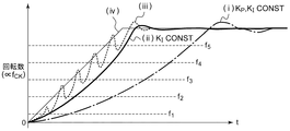
本実施の形態のように、ステッピングモータをDCモータに置換したプラットフォームにおいても、上位コントローラ104からのクロック周波数fCKは、台形波状に変化することが想定される。図16は、クロック信号CLKの周波数fCKの波形図である。(i)〜(iii)は、定速時の回転数が異なることを示す。
Even in the platform in which the stepping motor is replaced with the DC motor as in the present embodiment, the clock frequency f CK from the
上述のように、フィードバックコントローラ330は、PI制御器を含み、その制御特性は、比例ゲインKPと積分ゲインKIで規定される。実施の形態に係るフィードバックコントローラ330は、クロック周波数fCKに応じて制御特性(比例ゲイン、積分ゲインの少なくとも一方)を動的に変化させる。これにより、制御特性を固定した場合に比べて、モータの追従性を高めることができる。
As mentioned above, the
フィードバックコントローラ330は、クロック周波数fCKと、制御特性(比例ゲイン、積分ゲイン)の関係を保持するテーブルをメモリに保持している。
The
より好ましくはDCモータの回転開始後、クロック周波数fCKの上昇中に、積分ゲインKIを一定とし、比例ゲインKPのみをクロック周波数fCKに応じて変化させるとよい。比例ゲインKPはクロック周波数fCKに対して、正の相関を有し、単調増加してもよい。 More preferably, after the start of rotation of the DC motor, while the clock frequency f CK is rising, the integral gain K I may be fixed and only the proportional gain K P may be changed according to the clock frequency f CK . The proportional gain K P has a positive correlation with the clock frequency f CK and may be monotonically increasing.
図17は、モータ駆動システム100の始動時のモータの回転数を示す図である。(i)は、制御特性を固定したときの波形を、(ii)は、比例ゲインKPのみを変化させたときの波形を、(iii)は、比例ゲインKP、積分ゲインKIの両方を変化させたときの波形を示す。(iv)はクロック周波数fCKにもとづく目標回転数である。f1,f2・・・・は、制御特性が切り替わるしきい値を示す。
FIG. 17 is a diagram showing the number of revolutions of the motor when the
(i)に示すように、制御特性を固定すると、回転数が目標回転数に到達するまでの時間が長くなる。一方で、(iii)に示すように、比例ゲインと積分ゲインの両方を、変化させると、積分ゲインKIを切りかえるタイミングにおいて、それまで蓄積されていた積分項が増大するため、回転数が振動する(回転ムラ)。そこで(ii)に示すように、積分ゲインを一定としつつ、比例ゲインのみを変化させることで、回転ムラを抑制しつつ、追従性を高めることができる。 As shown in (i), when the control characteristic is fixed, it takes a long time for the rotational speed to reach the target rotational speed. On the other hand, as shown in (iii), when both the proportional gain and the integral gain are changed, the integral term accumulated up to that point increases at the timing at which the integral gain K I is switched. Yes (uneven rotation). Therefore, as shown in (ii), by changing only the proportional gain while keeping the integral gain constant, it is possible to improve the followability while suppressing the rotation unevenness.
ここでは、回転数を上昇させるときの動作を説明したが、回転数を低下させる際も同様であり、積分ゲインKIを一定としながら、比例ゲインKPをクロック周波数fCKに応じて変化させるとよい。 Here, the operation for increasing the rotational speed has been described, but the same is true for reducing the rotational speed, and the proportional gain K P is changed according to the clock frequency f CK while keeping the integral gain K I constant. It is good.
(電子ギア)
続いて、電子ギアについて説明する。上位コントローラ104のスペックによっては、クロック信号CLKの周波数fCKの可変範囲が制約される場合がある。たとえば、クロック周波数fCKの上限fMAXが低いと、その上限fMAXでDCモータの回転数が制約される。上限周波数fMAXで規定される回転数よりも高い回転数でモータを回転させたい場合、従来では機械ギアを用いる必要があり、コストアップの要因となっていた。この問題を解消するために、駆動IC200は、電子ギアの機能を備える。
(Electronic gear)
Subsequently, the electronic gear will be described. Depending on the specifications of the
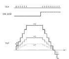
図18は、電子ギアの機能を説明する図である。上述のように、位置指令値生成部312においては、クロック信号CLKのエッジの個数が積算される。図6(a)〜(c)では、クロック信号CLKのエッジ1個あたりにつき、ターゲット値TGTが1ずつ、インクリメント、あるいはデクリメントされた。
FIG. 18 is a view for explaining the function of the electronic gear. As described above, in position command
これに対して、電子ギアを備えるロジック回路300Aでは、クロック信号CLKのエッジ1個たりにつきインクリメント/デクリメントする変化量ΔTGTが外部から設定可能である。図18では、ΔTGT=1,2,4の3段階で切りかえたときの動作を示す。 On the other hand, in the logic circuit 300A having an electronic gear, the change amount ΔTGT to be incremented / decremented can be externally set for each edge of the clock signal CLK. FIG. 18 shows the operation when three stages of ΔTGT = 1, 2 and 4 are switched.
変化量ΔTGTに応じて、クロック信号CLK1パルス当たりの、ロータの回転角を制御することができる。したがって変化量ΔTGTは、電子的なギア比に相当する。電子ギアの機能を実装することで、機械ギアを減らし、あるいは無くすことができるため、装置の低コスト化、小型化が可能であり、また装置の構造が簡素化できるため、故障のリスクを減らすことができる。 The rotation angle of the rotor per pulse of clock signal CLK can be controlled in accordance with change amount ΔTGT. Therefore, the change amount ΔTGT corresponds to an electronic gear ratio. By implementing the function of the electronic gear, it is possible to reduce or eliminate the mechanical gear, so that the cost and size of the device can be reduced, and the structure of the device can be simplified, thereby reducing the risk of failure. be able to.
図19は、電子ギアの機能を備える駆動IC200Aのブロック図である。駆動IC200Aには、電子ギアの設定のための設定ピンMODEが設けられ、この設定ピンMODEの状態に応じて、変化量ΔTGTが選択される。たとえば設定ピンMODEには、抵抗が外付け可能であり、設定ピンMODEには、抵抗の有無あるいは抵抗の抵抗値に応じた電圧VMODEが発生する。コンパレータCMP1あるいはA/Dコンバータ(不図示)によってこのモード電圧VMODEが検出され、モード電圧VMODEに応じた変化量ΔTGTが選択される。
FIG. 19 is a block diagram of a
より詳しくは、電子ギアの機能は、位置指令値生成部312に実装することができる。電子ギアの機能の実装について、図6(a)〜(c)を参照して説明する。たとえば図6(a)の位置指令値生成部312においては、カウンタ322のインクリメント、デクリメント量を、設定ピンMODEの状態に応じて変化させればよい。
More specifically, the function of the electronic gear can be implemented in the position command
図6(b)の位置指令値生成部312においては、演算器324の入力Aに与える値を、設定ピンMODEの状態に応じて、1,2,4…と多値で切りかえ可能とすればよい。
In position command
図6(c)の位置指令値生成部312においては、セレクタ327に入力する正負の2値を、設定ピンMODEの状態に応じて1倍、2倍、4倍・・・と切りかえ可能に構成すればよい。
In the position command
なお、ギア比に相当する変化量ΔTGTの設定方法は、設定ピンMODEを利用したものに限定されず、I2C(Inter IC)インタフェースや、SPI(Serial Peripheral Interface)などを利用して、レジスタに設定値を書き込むようにしてもよい。 The method of setting change amount ΔTGT corresponding to the gear ratio is not limited to the one using setting pin MODE, but may be a register using I 2 C (Inter IC) interface, SPI (Serial Peripheral Interface), etc. The set value may be written to
なお、ΔTGTの値は、1,2,4・・・には限定されず、任意の整数であってもよい。あるいは、ΔTGTは、1/2,1/4,1/8・・・、あるいは任意の分数であってもよい。ΔTGT<1とすることで、減速制御が可能となる。 The value of ΔTGT is not limited to 1, 2, 4... And may be any integer. Alternatively, ΔTGT may be 1/2, 1/4, 1/8 ... or any fraction. By setting ΔTGT <1, deceleration control is possible.
図20は、電子ギアの機能を備える駆動IC200Bのブロック図である。駆動IC200Bでは、ターゲット値TGTの変化量は一定であり、EN_A,EN_Bのパルス当たりのフィードバック値FBの変化量ΔFBが変更可能となっている。ΔFBは、整数あるいは非整数の任意の値に決めることができる。EN_A(EN_B信号)の1パルス当たりのΔFBを大きくすると、回転数は遅くできる。反対にEN_A(EN_B信号)の1パルス当たりのΔFBを小さくすると、回転数を速めることができる。ギア比選択部360は図19のコンパレータCMP1(あるいはA/Dコンバータ)に相当するブロックであり、設定ピンMODEの状態に応じてΔFBを選択する。
FIG. 20 is a block diagram of a
(用途)
図21は、モータ駆動システム100を備える電子機器を示す図である。図21には、電子機器900の一例として、プリンタを示す。電子機器900は、複数のDCモータ902、904を備える。たとえばDCモータ902は、プリントヘッド910の駆動機構912に用いられる。DCモータ904は、用紙送りの駆動機構914に用いられる。
(Use)
FIG. 21 is a diagram showing an electronic device provided with the
なおモータ駆動システム100の用途はプリンタには限定されず、さまざまなOA機器、産業機器、産業機械に用いることができる。
The application of the
以上、本発明について、実施の形態をもとに説明した。この実施の形態は例示であり、それらの各構成要素や各処理プロセスの組み合わせにいろいろな変形例が可能なこと、またそうした変形例も本発明の範囲にあることは当業者に理解されるところである。以下、こうした変形例について説明する。 The present invention has been described above based on the embodiments. It is understood by those skilled in the art that this embodiment is an exemplification, and that various modifications can be made to the combination of each component and each processing process, and such a modification is also within the scope of the present invention. is there. Hereinafter, such modifications will be described.
(変形例1)
実施の形態では、ホールセンサを用いたモータ駆動を説明したが、センサレスであってもよい。この場合、駆動IC200に、逆起電力を検出するコンパレータを実装すればよい。
(Modification 1)
Although the motor drive using a Hall sensor has been described in the embodiment, it may be sensorless. In this case, a comparator for detecting a back electromotive force may be mounted on the
(変形例2)
実施の形態では、ドライバ106のハイサイドトランジスタのゲート駆動電圧を得るためにチャージポンプを利用したが、ブートストラップ回路を内蔵してもよい。なおドライバ106のハイサイドトランジスタは、Pチャンネルであってもよく、この場合チャージポンプは不要である。
(Modification 2)
Although the charge pump is used to obtain the gate drive voltage of the high side transistor of the
(変形例3)
実施の形態では、ドライバ106が駆動IC200に外付けされたが、ドライバ106を駆動IC200に集積化してもよい。反対に、実施の形態では、プリドライバ250が駆動IC200に集積化されたが、プリドライバ250を駆動IC200の外部に設けてもよく、たとえばドライバ106とプリドライバ250を集積化してもよい。
(Modification 3)
In the embodiment, the
(変形例4)
実施の形態では、駆動ICをロジック回路で実装したが、その限りでなく、ロジック回路300で示されるブロックを、プロセッサ(CPUやマイコン)とソフトウェアプログラムの組み合わせで構成してもよい。
(Modification 4)
In the embodiment, the drive IC is implemented by a logic circuit. However, the present invention is not limited to this. The block indicated by the
100 モータ駆動システム
102 DCモータ
104 上位コントローラ
106 ドライバ
110 ホールセンサ
112 エンコーダ
200 駆動IC
BUF 入力バッファ
HCMP ホールコンパレータ
250 プリドライバ
260 電源回路群
262 オペアンプ
264 基準電圧源
266 チャージポンプ
268,270 電源回路
280 保護回路
300 ロジック回路
310 誤差検出器
312 位置指令値生成部
314 位置検出値生成部
316 減算器
320 エッジ検出回路
322 アップダウンカウンタ
324 演算器
325 メモリ
326 オペコードセレクタ
327 セレクタ
328 加算器
329 メモリ
330 フィードバックコントローラ
340 駆動信号生成部
342 パルス幅変調器
344 通電ロジック
360 ギア比選択部
100
BUF input buffer
Claims (24)
上位コントローラからのクロック信号と、エンコーダからのパルス信号と、を受け、前記パルス信号にもとづく前記DCモータのロータの現在位置と、前記クロック信号にもとづく前記ロータの目標位置との差分である位置誤差値を生成する誤差検出器と、
ロジック回路で構成され、前記位置誤差値がゼロに近づくように指令値を生成するフィードバックコントローラと、
ロジック回路で構成され、前記指令値に応じた駆動信号を生成する駆動信号生成部と、
を備え、ひとつの半導体基板に集積化されることを特徴とする駆動回路。 DC motor drive circuit,
A position error which is a difference between a current position of the rotor of the DC motor based on the pulse signal and a target position of the rotor based on the clock signal in response to a clock signal from the host controller and a pulse signal from the encoder An error detector that produces a value;
A feedback controller, which comprises a logic circuit, and generates a command value so that the position error value approaches zero;
A drive signal generation unit configured by a logic circuit and generating a drive signal according to the command value;
And a driving circuit characterized in that the driving circuit is integrated on one semiconductor substrate.
前記クロック信号のエッジの個数の積算値に応じたターゲット値を生成する位置指令値生成部と、
前記パルス信号にもとづき、前記ロータの現在位置を示すフィードバック値を生成する位置検出値生成部と、
前記ターゲット値と前記フィードバック値の差分を生成する減算器と、
を含むことを特徴とする請求項1から4のいずれかに記載の駆動回路。 The error detector
A position command value generation unit that generates a target value according to an integrated value of the number of edges of the clock signal;
A position detection value generation unit that generates a feedback value indicating the current position of the rotor based on the pulse signal;
A subtractor that generates a difference between the target value and the feedback value;
The drive circuit according to any one of claims 1 to 4, further comprising:
前記DCモータを駆動するインバータを含むドライバと、
前記ドライバを制御する請求項1から9のいずれかに記載の駆動回路と、
を備えることを特徴とする電子機器。 DC motor,
A driver including an inverter for driving the DC motor;
The drive circuit according to any one of claims 1 to 9, which controls the driver.
An electronic device comprising:
前記クロック信号にもとづく前記ロータの目標位置を示す位置指令値と、前記パルス信号にもとづく前記ロータの現在位置を示す位置検出値との差分に応じた位置誤差値を生成する誤差検出器と、
前記位置誤差値がゼロに近づくようにトルク指令値を生成するフィードバックコントローラと、
前記トルク指令値に応じた駆動信号を生成する駆動信号生成部と、
を備え、
回転制御モードと保持モードが切りかえ可能であり、前記回転制御モードと前記保持モードとで、前記フィードバックコントローラの制御特性および前記駆動信号生成部における前記駆動信号の生成方法の少なくとも一方が切り替わることを特徴とする駆動回路。 A driving circuit for driving a DC motor according to a clock signal from a host controller and a pulse signal indicating the position of a rotor of the DC motor from an encoder,
An error detector that generates a position error value according to a difference between a position command value indicating the target position of the rotor based on the clock signal and a position detection value indicating the current position of the rotor based on the pulse signal;
A feedback controller that generates a torque command value such that the position error value approaches zero;
A drive signal generation unit that generates a drive signal according to the torque command value;
Equipped with
A rotation control mode and a holding mode can be switched, and at least one of a control characteristic of the feedback controller and a method of generating the drive signal in the drive signal generation unit is switched between the rotation control mode and the holding mode. Drive circuit.
前記回転制御モードと前記保持モードとで、前記PI制御器の比例ゲインと積分ゲインの少なくとも一方が異なることを特徴とする請求項11に記載の駆動回路。 The feedback controller includes a PI (Proportional Integral) controller,
The drive circuit according to claim 11, wherein at least one of a proportional gain and an integral gain of the PI controller is different between the rotation control mode and the holding mode.
前記トルク指令値に応じたデューティ比を有するPWM(Pulse Width Modulation)信号を生成するパルス幅変調器と、
前記PWM信号とホールコンパレータの出力とにもとづいて前記駆動信号を生成する通電ロジックと、
を含むことを特徴とする請求項11から18のいずれかに記載の駆動回路。 The drive signal generation unit
A pulse width modulator that generates a PWM (Pulse Width Modulation) signal having a duty ratio corresponding to the torque command value;
Energizing logic that generates the drive signal based on the PWM signal and the output of the Hall comparator;
The drive circuit according to any one of claims 11 to 18, comprising:
前記DCモータを駆動するインバータを含むドライバと、
前記ドライバを制御する請求項11から21のいずれかに記載の駆動回路と、
を備えることを特徴とする電子機器。 DC motor,
A driver including an inverter for driving the DC motor;
The drive circuit according to any one of claims 11 to 21, which controls the driver.
An electronic device comprising:
上位コントローラからのクロック信号にもとづき、前記DCモータのロータの目標位置を示す位置指令値を生成するステップと、
エンコーダからのDCモータのロータの位置を示すパルス信号にもとづき、前記ロータの現在位置を示す位置検出値を生成するステップと、
回転制御モードと保持モードを選択するステップと、
前記位置検出値と前記位置指令値の誤差がゼロに近づくように、トルク指令値を生成するステップであって、前記回転制御モードと前記保持モードとで、制御特性が異なるステップと、
を備えることを特徴とする駆動方法。 A method of driving a DC motor,
Generating a position command value indicating a target position of the rotor of the DC motor based on a clock signal from a host controller;
Generating a position detection value indicating the current position of the rotor based on a pulse signal indicating the position of the rotor of the DC motor from the encoder;
Selecting a rotation control mode and a holding mode;
Generating a torque command value such that an error between the position detection value and the position command value approaches zero, wherein control characteristics differ between the rotation control mode and the holding mode;
A driving method comprising:
上位コントローラからのクロック信号にもとづき、前記DCモータのロータの目標位置を示す位置指令値を生成するステップと、
エンコーダからのDCモータのロータの位置を示すパルス信号にもとづき、前記ロータの現在位置を示す位置検出値を生成するステップと、
前記位置検出値と前記位置指令値の誤差がゼロに近づくように、トルク指令値を生成するステップと、
回転制御モードと保持モードを選択するステップと、
前記トルク指令値にもとづいてインバータの状態を規定する駆動信号を生成するステップであって、前記回転制御モードと前記保持モードとで、前記駆動信号の生成方法が異なるステップと、
を備えることを特徴とする駆動方法。 A method of driving a DC motor,
Generating a position command value indicating a target position of the rotor of the DC motor based on a clock signal from a host controller;
Generating a position detection value indicating the current position of the rotor based on a pulse signal indicating the position of the rotor of the DC motor from the encoder;
Generating a torque command value such that an error between the position detection value and the position command value approaches zero;
Selecting a rotation control mode and a holding mode;
Generating a drive signal that defines the state of the inverter based on the torque command value, wherein the method of generating the drive signal differs between the rotation control mode and the holding mode;
A driving method comprising:
Priority Applications (1)
| Application Number | Priority Date | Filing Date | Title |
|---|---|---|---|
| US16/176,412 US10879819B2 (en) | 2017-11-02 | 2018-10-31 | Driving circuit and driving method for DC motor |
Applications Claiming Priority (4)
| Application Number | Priority Date | Filing Date | Title |
|---|---|---|---|
| JP2017213091 | 2017-11-02 | ||
| JP2017213089 | 2017-11-02 | ||
| JP2017213089 | 2017-11-02 | ||
| JP2017213091 | 2017-11-02 |
Publications (2)
| Publication Number | Publication Date |
|---|---|
| JP2019088185A true JP2019088185A (en) | 2019-06-06 |
| JP7311957B2 JP7311957B2 (en) | 2023-07-20 |
Family
ID=66763574
Family Applications (1)
| Application Number | Title | Priority Date | Filing Date |
|---|---|---|---|
| JP2018200011A Active JP7311957B2 (en) | 2017-11-02 | 2018-10-24 | DC motor drive circuit and electronic equipment using the same |
Country Status (1)
| Country | Link |
|---|---|
| JP (1) | JP7311957B2 (en) |
Cited By (1)
| Publication number | Priority date | Publication date | Assignee | Title |
|---|---|---|---|---|
| CN117914184A (en) * | 2023-12-21 | 2024-04-19 | 中国第一汽车股份有限公司 | Brushless DC motor and control method, control device and computer storage medium |
Citations (8)
| Publication number | Priority date | Publication date | Assignee | Title |
|---|---|---|---|---|
| JPH03150610A (en) * | 1989-11-08 | 1991-06-27 | Mitsubishi Heavy Ind Ltd | Servo controller with lost motion correcting function |
| JPH0947059A (en) * | 1995-07-27 | 1997-02-14 | Fuji Xerox Co Ltd | Speed controller for motor |
| JP2011114951A (en) * | 2009-11-26 | 2011-06-09 | Ricoh Co Ltd | Motor control apparatus, motor control system and image forming apparatus |
| JP2013094037A (en) * | 2011-10-27 | 2013-05-16 | Ricoh Co Ltd | Driving device and image forming apparatus provided with the same |
| JP2014039417A (en) * | 2012-08-17 | 2014-02-27 | Ricoh Co Ltd | Motor control device and motor control method, and image forming apparatus |
| JP2016171707A (en) * | 2015-03-13 | 2016-09-23 | ミネベア株式会社 | Motor drive control device and motor drive control system |
| JP2017184426A (en) * | 2016-03-30 | 2017-10-05 | ローム株式会社 | Driving circuit of three-phase motor, driving method, and printing device |
| JP2017192195A (en) * | 2016-04-12 | 2017-10-19 | 京セラドキュメントソリューションズ株式会社 | Motor control device, image formation device, motor control method, and method of controlling image formation device |
-
2018
- 2018-10-24 JP JP2018200011A patent/JP7311957B2/en active Active
Patent Citations (8)
| Publication number | Priority date | Publication date | Assignee | Title |
|---|---|---|---|---|
| JPH03150610A (en) * | 1989-11-08 | 1991-06-27 | Mitsubishi Heavy Ind Ltd | Servo controller with lost motion correcting function |
| JPH0947059A (en) * | 1995-07-27 | 1997-02-14 | Fuji Xerox Co Ltd | Speed controller for motor |
| JP2011114951A (en) * | 2009-11-26 | 2011-06-09 | Ricoh Co Ltd | Motor control apparatus, motor control system and image forming apparatus |
| JP2013094037A (en) * | 2011-10-27 | 2013-05-16 | Ricoh Co Ltd | Driving device and image forming apparatus provided with the same |
| JP2014039417A (en) * | 2012-08-17 | 2014-02-27 | Ricoh Co Ltd | Motor control device and motor control method, and image forming apparatus |
| JP2016171707A (en) * | 2015-03-13 | 2016-09-23 | ミネベア株式会社 | Motor drive control device and motor drive control system |
| JP2017184426A (en) * | 2016-03-30 | 2017-10-05 | ローム株式会社 | Driving circuit of three-phase motor, driving method, and printing device |
| JP2017192195A (en) * | 2016-04-12 | 2017-10-19 | 京セラドキュメントソリューションズ株式会社 | Motor control device, image formation device, motor control method, and method of controlling image formation device |
Cited By (1)
| Publication number | Priority date | Publication date | Assignee | Title |
|---|---|---|---|---|
| CN117914184A (en) * | 2023-12-21 | 2024-04-19 | 中国第一汽车股份有限公司 | Brushless DC motor and control method, control device and computer storage medium |
Also Published As
| Publication number | Publication date |
|---|---|
| JP7311957B2 (en) | 2023-07-20 |
Similar Documents
| Publication | Publication Date | Title |
|---|---|---|
| JP5410690B2 (en) | Brushless motor control device and brushless motor | |
| US8183807B2 (en) | Method of driving DC motor and related circuit for avoiding reverse current | |
| JP2011199968A (en) | Apparatus and method for control of brushless motor | |
| CN108155834B (en) | Motor drive control device and control method for motor drive control device | |
| US11290051B2 (en) | Motor control apparatus and control method of the same | |
| JP6392509B2 (en) | Motor control circuit | |
| US10879819B2 (en) | Driving circuit and driving method for DC motor | |
| CN113678363B (en) | Motor drive control device and motor drive control method | |
| JP5307997B2 (en) | Brushless DC motor drive device | |
| JP7311957B2 (en) | DC motor drive circuit and electronic equipment using the same | |
| JP6934394B2 (en) | DC motor drive circuit, drive method and electronic equipment using it | |
| JP2004166436A (en) | Electric fluid pump device | |
| JP7012507B2 (en) | DC motor drive circuit, drive method and electronic equipment using it | |
| CN107078679B (en) | Power conversion device and control method for power conversion device | |
| JP7249740B2 (en) | MOTOR DRIVE DEVICE, MOTOR SYSTEM, FAN MOTOR AND MOTOR DRIVING METHOD | |
| JP6698403B2 (en) | Motor drive circuit, printer device | |
| JP2009278734A (en) | Voltage control circuit and motor driving device | |
| JP4062228B2 (en) | DC motor drive device | |
| JP5399085B2 (en) | Brushless motor drive circuit, motor unit, and electronic device using the same | |
| US20240333111A1 (en) | Motor driver circuit and driving method, cooling device and electronic apparatus using the same | |
| CN115632578B (en) | Motor controller | |
| JP7777095B2 (en) | Motor drive control device and motor unit | |
| JP4695924B2 (en) | Motor drive device | |
| KR101244843B1 (en) | Counter electromotive force detector circuit of sensorless bldc motor and method thereof | |
| CN119675499A (en) | Motor drive devices, semiconductor devices |
Legal Events
| Date | Code | Title | Description |
|---|---|---|---|
| A621 | Written request for application examination |
Free format text: JAPANESE INTERMEDIATE CODE: A621 Effective date: 20210825 |
|
| A977 | Report on retrieval |
Free format text: JAPANESE INTERMEDIATE CODE: A971007 Effective date: 20220720 |
|
| A131 | Notification of reasons for refusal |
Free format text: JAPANESE INTERMEDIATE CODE: A131 Effective date: 20220802 |
|
| A521 | Request for written amendment filed |
Free format text: JAPANESE INTERMEDIATE CODE: A523 Effective date: 20220921 |
|
| A131 | Notification of reasons for refusal |
Free format text: JAPANESE INTERMEDIATE CODE: A131 Effective date: 20230117 |
|
| A521 | Request for written amendment filed |
Free format text: JAPANESE INTERMEDIATE CODE: A523 Effective date: 20230309 |
|
| TRDD | Decision of grant or rejection written | ||
| A01 | Written decision to grant a patent or to grant a registration (utility model) |
Free format text: JAPANESE INTERMEDIATE CODE: A01 Effective date: 20230704 |
|
| A61 | First payment of annual fees (during grant procedure) |
Free format text: JAPANESE INTERMEDIATE CODE: A61 Effective date: 20230707 |
|
| R150 | Certificate of patent or registration of utility model |
Ref document number: 7311957 Country of ref document: JP Free format text: JAPANESE INTERMEDIATE CODE: R150 |