JP2019197848A - Circuit structure and electric connection box - Google Patents
Circuit structure and electric connection box Download PDFInfo
- Publication number
- JP2019197848A JP2019197848A JP2018092072A JP2018092072A JP2019197848A JP 2019197848 A JP2019197848 A JP 2019197848A JP 2018092072 A JP2018092072 A JP 2018092072A JP 2018092072 A JP2018092072 A JP 2018092072A JP 2019197848 A JP2019197848 A JP 2019197848A
- Authority
- JP
- Japan
- Prior art keywords
- heat transfer
- heat
- pattern
- circuit structure
- resist layer
- Prior art date
- Legal status (The legal status is an assumption and is not a legal conclusion. Google has not performed a legal analysis and makes no representation as to the accuracy of the status listed.)
- Pending
Links
Images


Classifications
-
- H—ELECTRICITY
- H02—GENERATION; CONVERSION OR DISTRIBUTION OF ELECTRIC POWER
- H02G—INSTALLATION OF ELECTRIC CABLES OR LINES, OR OF COMBINED OPTICAL AND ELECTRIC CABLES OR LINES
- H02G3/00—Installations of electric cables or lines or protective tubing therefor in or on buildings, equivalent structures or vehicles
- H02G3/02—Details
- H02G3/08—Distribution boxes; Connection or junction boxes
- H02G3/16—Distribution boxes; Connection or junction boxes structurally associated with support for line-connecting terminals within the box
-
- H—ELECTRICITY
- H05—ELECTRIC TECHNIQUES NOT OTHERWISE PROVIDED FOR
- H05K—PRINTED CIRCUITS; CASINGS OR CONSTRUCTIONAL DETAILS OF ELECTRIC APPARATUS; MANUFACTURE OF ASSEMBLAGES OF ELECTRICAL COMPONENTS
- H05K1/00—Printed circuits
- H05K1/02—Details
-
- H—ELECTRICITY
- H05—ELECTRIC TECHNIQUES NOT OTHERWISE PROVIDED FOR
- H05K—PRINTED CIRCUITS; CASINGS OR CONSTRUCTIONAL DETAILS OF ELECTRIC APPARATUS; MANUFACTURE OF ASSEMBLAGES OF ELECTRICAL COMPONENTS
- H05K7/00—Constructional details common to different types of electric apparatus
- H05K7/20—Modifications to facilitate cooling, ventilating, or heating
-
- H—ELECTRICITY
- H10—SEMICONDUCTOR DEVICES; ELECTRIC SOLID-STATE DEVICES NOT OTHERWISE PROVIDED FOR
- H10W—GENERIC PACKAGES, INTERCONNECTIONS, CONNECTORS OR OTHER CONSTRUCTIONAL DETAILS OF DEVICES COVERED BY CLASS H10
- H10W40/00—Arrangements for thermal protection or thermal control
- H10W40/10—Arrangements for heating
-
- H—ELECTRICITY
- H10—SEMICONDUCTOR DEVICES; ELECTRIC SOLID-STATE DEVICES NOT OTHERWISE PROVIDED FOR
- H10W—GENERIC PACKAGES, INTERCONNECTIONS, CONNECTORS OR OTHER CONSTRUCTIONAL DETAILS OF DEVICES COVERED BY CLASS H10
- H10W70/00—Package substrates; Interposers; Redistribution layers [RDL]
- H10W70/60—Insulating or insulated package substrates; Interposers; Redistribution layers
Landscapes
- Engineering & Computer Science (AREA)
- Microelectronics & Electronic Packaging (AREA)
- Architecture (AREA)
- Civil Engineering (AREA)
- Structural Engineering (AREA)
- Physics & Mathematics (AREA)
- Thermal Sciences (AREA)
- Cooling Or The Like Of Electrical Apparatus (AREA)
- Cooling Or The Like Of Semiconductors Or Solid State Devices (AREA)
- Structure Of Printed Boards (AREA)
- Connection Or Junction Boxes (AREA)
Abstract
【課題】回路構成体11の放熱性を向上させる。【解決手段】本実施形態に係る回路構成体11は、FET26と、導電パターン22が形成された第1面21の導電パターン22にFET26が接続されており、第1面21と反対側に形成された第2面28には絶縁性の第2レジスト層31が形成されており、第2レジスト層31に開口された放熱窓部32から導電パターン22と伝熱的に接続された伝熱パターン33が露出している回路基板14と、第2レジスト層31よりも熱伝導率が高く、且つ、放熱窓部32から露出する伝熱パターン33に伝熱的に接続された第1伝熱部34と、第2レジスト層31よりも熱伝導率が高く、且つ、第1伝熱部34と伝熱的に接続された第2伝熱部35と、第2伝熱部35と伝熱的に接続するヒートシンク13と、を備える。【選択図】図1PROBLEM TO BE SOLVED: To improve the heat dissipation of a circuit structure 11. SOLUTION: In a circuit structure 11 according to the present embodiment, a FET 26 is connected to a conductive pattern 22 of a first surface 21 on which a conductive pattern 22 is formed, and the FET 26 is formed on the side opposite to the first surface 21. An insulative second resist layer 31 is formed on the exposed second surface 28, and a heat transfer pattern thermally conductively connected to the conductive pattern 22 from a heat dissipation window portion 32 opened in the second resist layer 31. The circuit board 14 having the exposed 33 and the second heat transfer layer 31 have a higher thermal conductivity than the second resist layer 31 and are thermally connected to the heat transfer pattern 33 exposed from the heat dissipation window 32. 34, a second heat transfer section 35 having a higher thermal conductivity than that of the second resist layer 31 and being heat transfer connected to the first heat transfer section 34, and a second heat transfer section 35 and a heat transfer And a heat sink 13 connected to. [Selection diagram] Figure 1
Description
本明細書に開示された技術は、回路構成体、及び電気接続箱に関する。 The technology disclosed in this specification relates to a circuit structure and an electrical junction box.
従来、回路基板に発熱部品が実装された回路構成体として、特開2014−170868号公報に記載のものが知られている。この回路構成体は、金属筐体の内部に収容されている。回路基板と金属筐体との間には、グリース状の放熱材が配されている。この放熱材は、回路基板と金属筐体の双方に接触している。これにより、通電時に発熱部品で発生した熱は、回路基板から放熱材を経て金属筐体へと伝達され、金属筐体から外部へと放散されることが期待された。 Conventionally, as a circuit structure in which a heat generating component is mounted on a circuit board, one described in Japanese Patent Application Laid-Open No. 2014-170868 is known. This circuit component is housed inside a metal housing. A grease-like heat dissipating material is disposed between the circuit board and the metal casing. This heat dissipation material is in contact with both the circuit board and the metal casing. As a result, it was expected that the heat generated in the heat-generating component when energized was transmitted from the circuit board to the metal casing through the heat dissipation material and dissipated from the metal casing to the outside.
回路基板の表面及び裏面には、絶縁性のレジスト層が形成されている。このレジスト層は比較的に熱抵抗が大きい。このため、従来技術においては、回路基板に形成された導電パターンと、グリース状の放熱材との間に、比較的に熱抵抗が大きなレジスト層が介在してしまうので、回路構成体の放熱性が十分ではなかった。 An insulating resist layer is formed on the front and back surfaces of the circuit board. This resist layer has a relatively large thermal resistance. For this reason, in the prior art, a resist layer having a relatively large thermal resistance is interposed between the conductive pattern formed on the circuit board and the grease-like heat dissipation material. Was not enough.
本明細書に開示された技術は上記のような事情に基づいて完成されたものであって、放熱性が向上した回路構成体、及び電気接続箱を提供することを目的とする。 The technology disclosed in the present specification has been completed based on the above circumstances, and an object thereof is to provide a circuit structure body and an electrical junction box with improved heat dissipation.
本明細書に開示された技術は、回路構成体であって、発熱部品と、導電パターンが形成された第1面の前記導電パターンに前記発熱部品が接続されており、前記第1面と反対側に形成された第2面には絶縁性のレジスト層が形成されており、前記レジスト層に開口された放熱窓部から前記導電パターンと伝熱的に接続された伝熱パターンが露出している回路基板と、前記レジスト層よりも熱伝導率が高く、且つ、前記放熱窓部から露出する前記伝熱パターンに伝熱的に接続された第1伝熱部と、前記レジスト層よりも熱伝導率が高く、且つ、前記第1伝熱部と伝熱的に接続された第2伝熱部と、前記第2伝熱部と伝熱的に接続するヒートシンクと、を備える。 The technology disclosed in the present specification is a circuit structure, wherein the heat generating component is connected to the conductive pattern on the first surface on which the conductive pattern is formed, and is opposite to the first surface. An insulating resist layer is formed on the second surface formed on the side, and a heat transfer pattern thermally connected to the conductive pattern is exposed from a heat dissipation window portion opened in the resist layer. A circuit board having a thermal conductivity higher than that of the resist layer and thermally connected to the heat transfer pattern exposed from the heat radiating window, and heat higher than that of the resist layer. A second heat transfer portion having high conductivity and thermally connected to the first heat transfer portion, and a heat sink thermally connected to the second heat transfer portion are provided.
また、本明細書に開示された技術は、電気接続箱であって、上記の回路構成体と、前記回路構成体に取り付けられて、前記回路基板を覆うカバーと、を備える。 The technology disclosed in the present specification is an electrical junction box, and includes the above-described circuit structure and a cover that is attached to the circuit structure and covers the circuit board.
通電時に発熱部品で発生した熱は、発熱部品が接続された導電パターンに伝達された後に、この導電パターンと伝熱的に接続された伝熱パターンへと伝導され、第1伝熱部にまで伝達され、更に、第1伝熱部と伝熱的に接続された第2伝熱部へと確実に伝達される。第2伝熱部に到達した熱は、第2伝熱部からヒートシンクへと伝達され、ヒートシンクから外部へと放散される。 The heat generated in the heat-generating component during energization is transferred to the conductive pattern to which the heat-generating component is connected, and then transferred to the heat transfer pattern that is thermally connected to the conductive pattern, and reaches the first heat transfer section. Then, it is reliably transmitted to the second heat transfer section that is connected in heat transfer with the first heat transfer section. The heat that has reached the second heat transfer section is transferred from the second heat transfer section to the heat sink and is dissipated from the heat sink to the outside.
第1伝熱部はレジスト層よりも熱伝導率が高いので、レジスト層を介して第2伝熱部に熱が伝達される場合に比べて、伝熱パターンから第2伝熱部へ熱を効率よく伝達することができる。これにより、発熱部品から、ヒートシンクを経て外部へと熱を効率よく放散することができるので、回路構成体の放熱性を向上させることができる。 Since the first heat transfer section has a higher thermal conductivity than the resist layer, heat is transferred from the heat transfer pattern to the second heat transfer section as compared with the case where heat is transferred to the second heat transfer section through the resist layer. It can be transmitted efficiently. Thereby, heat can be efficiently dissipated from the heat generating component to the outside through the heat sink, so that the heat dissipation of the circuit structure can be improved.
本明細書に開示された技術の実施態様としては以下の態様が好ましい。 The following aspects are preferred as embodiments of the technology disclosed in this specification.
前記第1伝熱部の前記伝熱パターンからの突出高さ寸法は、前記レジスト層の厚さ寸法と同じか、又は大きく設定されている。 The protruding height dimension of the first heat transfer portion from the heat transfer pattern is set to be equal to or larger than the thickness dimension of the resist layer.
上記の構成によれば、第1伝熱部の突出端部は、レジスト層よりもヒートシンク側に突出するようになっている。これにより、第1伝熱部は確実に第2伝熱部と接触することができるので、回路構成体の放熱性を確実に向上させることができる。 According to said structure, the protrusion edge part of a 1st heat-transfer part protrudes on the heat sink side rather than a resist layer. Thereby, since a 1st heat-transfer part can contact with a 2nd heat-transfer part reliably, the heat dissipation of a circuit structure body can be improved reliably.
前記ヒートシンクと前記回路基板との間にはスペーサが介在されている。 Spacers are interposed between the heat sink and the circuit board.
上記の構成によれば、ヒートシンクと回路基板との間隔をスペーサによって正確に設定できる。これにより、第2伝熱部と第1伝熱部との間に空隙が生じることを抑制することができる。この結果、回路構成体の放熱性をより向上させることができる。 According to said structure, the space | interval of a heat sink and a circuit board can be set correctly with a spacer. Thereby, it can suppress that a space | gap arises between a 2nd heat-transfer part and a 1st heat-transfer part. As a result, the heat dissipation of the circuit structure can be further improved.
前記第1伝熱部は、はんだからなる。 The first heat transfer part is made of solder.
上記の構成によれば、伝熱パターンと第1伝熱部とを、はんだ付けという簡易な手法により、確実に接続することができる。これにより、伝熱パターンと第1伝熱部との間の伝熱効率を向上させることができるので、回路構成体の放熱性をより向上させることができる。 According to said structure, a heat-transfer pattern and a 1st heat-transfer part can be reliably connected by the simple method of soldering. Thereby, since the heat-transfer efficiency between a heat-transfer pattern and a 1st heat-transfer part can be improved, the heat dissipation of a circuit structure body can be improved more.
前記第2伝熱部は、グリース状又はゲル状をなしている。 The second heat transfer part has a grease shape or a gel shape.
上記の構成によれば、第2伝熱部はグリース状又はゲル状をなしているので、第1伝熱部及びヒートシンクの形状に追従して容易に変形することができる。これにより、第1伝熱部と第2伝熱部の密着性が向上すると共に、第2伝熱部とヒートシンクとの密着性も向上するので、回路構成体の放熱性をより向上させることができる。 According to said structure, since the 2nd heat-transfer part has comprised the shape of grease or gel, it can deform | transform easily following the shape of a 1st heat-transfer part and a heat sink. As a result, the adhesion between the first heat transfer section and the second heat transfer section is improved, and the adhesion between the second heat transfer section and the heat sink is also improved, so that the heat dissipation of the circuit structure can be further improved. it can.
前記第2伝熱部は、シート状をなしている。 The second heat transfer part has a sheet shape.
上記の構成によれば、第2伝熱部はシート状をなしているので、取り扱いが容易である。これにより、回路構成体の製造効率を向上させることができる。 According to said structure, since the 2nd heat-transfer part has comprised the sheet form, handling is easy. Thereby, the manufacturing efficiency of a circuit structure can be improved.
複数の前記第1伝熱部が間隔を空けて形成されており、複数の前記第1伝熱部同士の間に侵入した前記第2伝熱が、前記伝熱パターンと伝熱的に接続している。 A plurality of the first heat transfer portions are formed at intervals, and the second heat transfer that has entered between the plurality of first heat transfer portions is connected to the heat transfer pattern in a heat transfer manner. ing.
上記の構成によれば、伝熱パターンから第2伝熱部へと熱が伝達される経路が形成されるので、回路構成体の放熱性をより向上させることができる。 According to said structure, since the path | route through which heat is transmitted from a heat-transfer pattern to a 2nd heat-transfer part is formed, the heat dissipation of a circuit structure body can be improved more.
前記導電パターンと前記伝熱パターンとを連結するサーマルビアホールを有する。 A thermal via hole connecting the conductive pattern and the heat transfer pattern;
上記の構成によれば、導電パターンから伝熱パターンへの熱伝導の効率を向上させることができるので、回路構成体の放熱性をより向上させることができる。 According to said structure, since the efficiency of the heat conduction from a conductive pattern to a heat-transfer pattern can be improved, the heat dissipation of a circuit structure body can be improved more.
本明細書に開示された技術によれば、回路構成体、及び電気接続箱の放熱性を向上させることができる。 According to the technique disclosed in this specification, the heat dissipation of the circuit structure and the electrical junction box can be improved.
<実施形態1>
本明細書に開示された技術の実施形態1を、図1から図3を参照しつつ説明する。本実施形態に係る電気接続箱10は、回路構成体11を有する。電気接続箱10は、車両(図示せず)に搭載されて、電源(図示せず)と機器(図示せず)との間に配設される。以下の説明においては、複数の同一部材については、一部の部材にのみ符号を付して、他の部材については符号を省略する場合がある。
<Embodiment 1>
Embodiment 1 of the technique disclosed in this specification will be described with reference to FIGS. 1 to 3. The
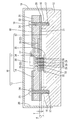
図1に示すように、電気接続箱10は、回路構成体11にカバー12が組み付けられてなる。回路構成体11は、ヒートシンク13と、ヒートシンク13に固定された回路基板14と、を有する。
As shown in FIG. 1, the
本実施形態においては、ヒートシンク13は金属製であって、底壁15と、底壁15の上面から上方に突出するボス16(スペーサの一例)と、を有する。ボス16は、筒形状をなしている。ボス16の上面には、下方に延びるネジ孔17が形成されている。ヒートシンク13を構成する金属としては、アルミニウム、アルミニウム合金、鉄、ステンレス、銅、銅合金等、必要に応じて任意の金属を適宜に選択することができる。なお、ヒートシンク13は、放熱性を有する合成樹脂製であってもよい。
In the present embodiment, the
カバー12は、上壁18と、上壁18の側縁から下方に延びる側壁19と、を備える。側壁19は、ヒートシンク13の底壁15に外嵌される。カバー12とヒートシンク13とは、ヒートシンク13の底壁15の側縁から突出するロック突部(図示せず)と、カバー12の側壁19に形成された弾性変形可能なロック受け部(図示せず)とが、弾性的に係合することにより一体に組み付けられる。また、カバー12とヒートシンク13とは、ネジ止めにより一体に組み付けられてもよい。このように、カバー12とヒートシンク13とは公知の手法により一体に組み付けられるようになっている。
The
ヒートシンク13とカバー12とが一体に組み付けられた状態で、ヒートシンク13の底壁15の上方であって、カバー12の上壁18の下方の領域は、回路基板14が収容される収容空間20とされる。
In a state where the
回路基板14は、絶縁性の合成樹脂からなる絶縁板に、プリント配線技術により金属製のパターンを形成してなる。回路基板14の上側の位置する第1面21には導電パターン22が形成されている。詳細には図示しないが、導電パターン22は回路を形成している。
The
回路基板14はボルト23が貫通される貫通孔24を有する。回路基板14がヒートシンク13のボス16の上面に載置された状態で、回路基板14の貫通孔24に挿通されたボルト23がボス16に形成されたネジ孔17に螺合されることにより、回路基板14がヒートシンク13に固定されている。
The
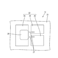
図2に示すように、回路基板14の第1面21には複数のランド25(導電パターン22の一例)が形成されている。ランド25には、FET26(Field effect transistor)のリード27がはんだ付け等の公知の手法により電気的に接続されている。FET26は発熱部品の一例である。発熱部品としては、リレー、コンデンサ、コイル、マイコン等、通電時に発熱する部品が例示される。
As shown in FIG. 2, a plurality of lands 25 (an example of a conductive pattern 22) are formed on the
なお、回路基板14に形成されたランド25には、発熱部品の他に、抵抗、ダイオード等の図示しない電子部品が接続されている。ランド25は上方から見て略長方形状をなしている。回路基板14の第1面21には、絶縁性材料からなる第1レジスト層60が形成されている。第1レジスト層60は、概ねランド25と異なる領域に形成されているが、ランド25の一部に重なって形成されていてもよい。
The
FET26の側縁からは、2本のリード27が外方に突出している。2本のリード27の一方はゲート端子であり、他方はドレイン端子である。FET26の下面には、ソース端子が形成されている。FET26のゲート端子、ドレイン端子、及びソース端子は回路基板14の上面に形成されたランド25にはんだ付けされている。
Two leads 27 protrude outward from the side edge of the
本実施形態に係る回路基板14は、電気的に絶縁状態で積層された複数層の導電パターン22を有する。回路基板14の下側に位置する第2面28には、第1面21に形成されたランド25と、複数(本実施形態では3個)のサーマルビアホール29によって伝熱的に接続された伝熱パターン33が形成されている。サーマルビアホール29は、回路基板14の第1面21と第2面28とを貫通する貫通孔24内に、熱伝導性を有する伝熱部30が充填されている。伝熱部30は、化学めっき、金属粉を含有する合成樹脂材を硬化させたもの等、公知の手法により形成することができる。伝熱部30の熱伝導性は、回路基板14を構成する絶縁性の合成樹脂よりも高い。
The
図2に示すように、回路基板14の第2面28には、絶縁性の第2レジスト層31(レジスト層の一例)が形成されている。第2レジスト層31には、下方に開口する放熱窓部32が形成されている。放熱窓部32からは、上記した伝熱パターン33が露出している。放熱窓部32は下方から見て略長方形状をなしている。
As shown in FIG. 2, an insulating second resist layer 31 (an example of a resist layer) is formed on the
伝熱パターン33には、第1伝熱部34が伝熱的に接続されている。第1伝熱部34は、金属、合成樹脂、セラミック等、必要に応じて任意の材料を適宜に選択することができる。第1伝熱部34の熱伝導率は第2レジスト層31よりも高く設定されている。本実施形態に係る第1伝熱部34は、はんだからなる。第1伝熱部34は、例えば、伝熱パターン33にクリームはんだを塗布後、加熱によりクリームはんだを溶融し、その後、固化させることにより形成することができる。
A first
第1伝熱部34は、下方から見て、角の丸められた長方形状をなしている。第1伝熱部34の外形状は、伝熱パターン33の外形状よりもやや小さく形成されている。
The first
第1伝熱部34の下方には、第2伝熱部35が配されている。第2伝熱部35の熱伝導率は、第2レジスト層31よりも高く設定されている。第2伝熱部35は導体でもよいし、また、絶縁性を有していてもよい。第2伝熱部35は、シート状又はフィルム状をなしていてもよいし、グリース状又はゲル状をなしていてもよい。第2伝熱部35は、少なくとも回路基板14をヒートシンク13に固定する工程においてはグリース状又はゲル状をなしていて、回路基板14とヒートシンク13とを固定した後においては固化するものであってもよい。また、回路基板14をヒートシンク13に固定する工程の前後を通じてグリース状又はゲル状であってもよい。第2伝熱部35は、熱伝導率の高いフィラーを含んでいてもよい。
A second
本実施形態に係る第2伝熱部35は、絶縁性の合成樹脂であって、回路基板14をヒートシンク13に固定する工程においてはグリース状又はゲル状をなしており、回路基板14をヒートシンク13に固定した後においては、固化するようになっている。
The second
第1伝熱部34の、伝熱パターン33の下面からの、下方への突出高さ寸法Hは、第2レジスト層31の厚さ寸法Tと、同じか、又は大きく設定されている。本実施形態においては、第1伝熱部34の伝熱パターン33からの突出高さ寸法Hは、第2レジスト層31の厚さ寸法Tよりも大きく設定されている。
The downward protruding height dimension H of the first
製造工程
続いて、本実施形態に係る電気接続箱10の製造工程の一例を説明する。電気接続箱10の製造工程は、以下の記載に限定されない。
Manufacturing Process Subsequently, an example of a manufacturing process of the
回路基板14の第2面28に形成された伝熱パターン33に、クリームはんだを公知のスクリーン印刷により塗布する。その後、回路基板14をリフロー炉で加熱することにより、伝熱パターン33に第1伝熱部34を形成する。
Cream solder is applied to the
回路基板14の第1面21に形成されたランド25に、クリームはんだを公知のスクリーン印刷により塗布する。FET26を含む電子部品を載置する。回路基板14をリフロ―炉で加熱することにより、ランド25と、FET26を含む電子部品とを接続する。
Cream solder is applied to the
ヒートシンク13のうち、回路基板14の第2面28に形成された第1伝熱部34に対応する部分に、グリース状又はゲル状の第2伝熱部35を塗布する。回路基板14をヒートシンク13のボス16の上面に載置する。回路基板14の貫通孔24内にボルト23を挿通させつつ、このボルト23をボス16に形成されたネジ孔17に螺合させる。ボルト23を螺合することにより回路基板14がヒートシンク13に接近すると、回路基板14の第2面28に配された第1伝熱部34が上方から第2伝熱部35に接触する。更にボルト23を螺合することにより回路基板14をヒートシンク13に固定する。これにより回路構成体11が完成する。
A grease-like or gel-like second
続いて、カバー12を上方からヒートシンク13に組み付ける。これにより電気接続箱10が完成する。
Subsequently, the
本実施形態の作用効果
続いて、本実施形態の作用効果について説明する。本実施形態に係る回路構成体11は、FET26と、導電パターン22が形成された第1面21の導電パターン22にFET26が接続されており、第1面21と反対側に形成された第2面28には絶縁性の第2レジスト層31が形成されており、第2レジスト層31に開口された放熱窓部32から導電パターン22と伝熱的に接続された伝熱パターン33が露出している回路基板14と、第2レジスト層31よりも熱伝導率が高く、且つ、放熱窓部32から露出する伝熱パターン33に伝熱的に接続された第1伝熱部34と、第2レジスト層31よりも熱伝導率が高く、且つ、第1伝熱部34と伝熱的に接続された第2伝熱部35と、第2伝熱部35と伝熱的に接続するヒートシンク13と、を備える。
Operational Effects of the Present Embodiment Next, operational effects of the present embodiment will be described. In the
まず、本実施形態の効果を説明するために、仮想的な技術に係る電気接続箱110を図6に示す。電気接続箱110は回路構成体111を有する。回路構成体111に含まれる回路基板114の上面には第1レジスト層160が形成されており、回路基板114の下面には第2レジスト層131が形成されている。第2レジスト層131の一部を剥がすことにより回路基板114に形成された伝熱パターン133が露出している。この伝熱パターン133に対応する位置にグリース状の第2伝熱部135が配されている。なお、符号については、特に言及しない限り、実施形態1に係る部材に付した符号に、100を加えたものを用いた。
First, in order to explain the effect of this embodiment, an
上記の技術によると、第2レジスト層131の厚みのために第2伝熱部135が伝熱パターン133にまで到達せず、むしろ、伝熱パターン133と第2伝熱部135との間に空気層が形成されてしまう。このため、上記の仮想的な技術によっては、回路構成体111の放熱性を十分に向上させることはできないのである。
According to the above technique, the second
これに対して本実施形態においては、通電時にFET26で発生した熱は、FET26が接続されたランド25(導電パターン22)に伝達された後に、このランド25と伝熱的に接続された伝熱パターン33へと伝導され、第1伝熱部34にまで伝達され、更に、第1伝熱部34と伝熱的に接続された第2伝熱部35へと確実に伝達される。第2伝熱部35に到達した熱は、第2伝熱部35からヒートシンク13へと伝達され、ヒートシンク13から外部へと放散される。
On the other hand, in the present embodiment, the heat generated in the
第1伝熱部34は第2レジスト層31よりも熱伝導率が高いので、第2レジスト層31を介して第2伝熱部35に熱が伝達される場合に比べて、伝熱パターン33から第2伝熱部35へ熱を効率よく伝達することができる。これにより、FET26から、ヒートシンク13を経て外部へと熱を効率よく放散することができるので、回路構成体11の放熱性を向上させることができる。
Since the first
本実施形態によれば、第1伝熱部34の伝熱パターン33からの突出高さ寸法Hは、第2レジスト層31の厚さ寸法Tと同じか、又は大きく設定されている。
According to the present embodiment, the protruding height dimension H of the first
上記の構成によれば、第1伝熱部34の突出端部は、第2レジスト層31よりもヒートシンク13側に突出するようになっている。これにより、第1伝熱部34は確実に第2伝熱部35と接触することができるので、回路構成体11の放熱性を確実に向上させることができる。
According to said structure, the protrusion edge part of the 1st heat-
本実施形態によれば、ヒートシンク13と回路基板14との間には、ヒートシンク13から回路基板14に向けて突出するボス16が介在している。
According to the present embodiment, the
上記の構成によれば、ヒートシンク13と回路基板14との間隔をボス16の高さ寸法によって正確に設定できる。これにより、グリース状又はゲル状をなす第2伝熱部35の充填量を正確に見積もることができるので、第2伝熱部35と第1伝熱部34との間に空隙が生じることを抑制することができる。この結果、回路構成体11の放熱性をより向上させることができる。
According to the above configuration, the distance between the
本実施形態によれば、第1伝熱部34は、はんだからなる。
According to this embodiment, the 1st heat-
上記の構成によれば、伝熱パターン33と第1伝熱部34とを確実に接続することができる。これにより、伝熱パターン33と第1伝熱部34との間の伝熱効率を向上させることができるので、回路構成体11の放熱性をより向上させることができる。
According to said structure, the heat-
本実施形態によれば、第2伝熱部35は、グリース状又はゲル状をなしている。
According to this embodiment, the 2nd heat-
上記の構成によれば、第2伝熱部35はグリース状又はゲル状をなしているので、第1伝熱部34及びヒートシンク13の形状に追従して容易に変形することができる。これにより、第1伝熱部34と第2伝熱部35の密着性が向上すると共に、第2伝熱部35とヒートシンク13との密着性も向上するので、回路構成体11の放熱性をより向上させることができる。
According to said structure, since the 2nd heat-
本実施形態によれば、導電パターン22と伝熱パターン33とはサーマルビアホール29によって連結されている。
According to the present embodiment, the
上記の構成によれば、導電パターン22から伝熱パターン33への熱伝導の効率を向上させることができるので、回路構成体11の放熱性をより向上させることができる。
According to said structure, since the efficiency of the heat conduction from the
<実施形態2>
次に、本明細書に開示された技術の実施形態2を、図4を参照しつつ説明する本実施形態に係る回路基板40においては、伝熱パターン33の下面には、複数の第1伝熱部41が、間隔を空けて離散した状態で形成されている。各第1伝熱部41は、下方から見て、略長方形状をなしている。本実施形態においては、図4における上下方向について間隔を空けて複数(本実施形態では6個)の第1伝熱部41が並ぶ第1伝熱部列42が、図4における左右方向に間隔を空けて複数(本実施形態では3列)並んで形成されている。
<Embodiment 2>
Next, in the
複数の第1伝熱部41同士の間に形成された隙間43内に、グリース状又はゲル状をなす第2伝熱部35が侵入することができるようになっている。上記の隙間43内に侵入した第2伝熱部35は伝熱パターン33と直接に接触するようになっている。
The second
上記以外の構成については、実施形態1と略同様なので、同一部材については同一符号を付し、重複する説明を省略する。 Since the configuration other than the above is substantially the same as that of the first embodiment, the same members are denoted by the same reference numerals, and redundant description is omitted.
本実施形態によれば、第2伝熱部35は、第1伝熱部41に押圧されることにより、隙間43の内部へと移動する。これにより、第2伝熱部35のうち第1伝熱部41に対応する位置に空気の泡が存在した場合でも、この空気の泡は、第1伝熱部41に押圧されて、空気の泡の周囲に存在する第2伝熱部35と共に隙間43内へ移動する。この結果、第2伝熱部35のうち第1伝熱部41に対応する位置からは空気が排除され、第1伝熱部41と第2伝熱部35とを確実に接触させることができる。これにより、回路構成体11の放熱性を向上させることができる。
According to the present embodiment, the second
また、隙間43内に移動した第2伝熱部35のうち伝熱パターン33と直接に接触するものについては、伝熱パターン33から第2伝熱部35へと熱が直接に伝達される経路が形成されるので、回路構成体11の放熱性をより向上させることができる。
Further, for the second
<実施形態3>
次に、本明細書に開示された技術の実施形態3を、図5を参照しつつ説明する。本実施形態に係る回路基板50においては、伝熱パターン33の下面には、複数(本実施形態では6個)の第1伝熱部51が、図5における上下方向について間隔を空けて並んで形成されている。各第1伝熱部51は、下方から見て、略長方形状をなしている。
<Embodiment 3>
Next, a third embodiment of the technique disclosed in this specification will be described with reference to FIG. In the
複数の第1伝熱部51同士の間に形成された隙間52内に、グリース状又はゲル状をなす第2伝熱部35が侵入することができるようになっている。上記の隙間52内に侵入した第2伝熱部35は伝熱パターン33と直接に接触するようになっている。
The second
上記以外の構成については、実施形態1と略同様なので、同一部材については同一符号を付し、重複する説明を省略する。 Since the configuration other than the above is substantially the same as that of the first embodiment, the same members are denoted by the same reference numerals, and redundant description is omitted.
本実施形態によれば、第2伝熱部35は、第1伝熱部51に押圧されることにより、隙間52の内部へと移動する。これにより、第2伝熱部35のうち第1伝熱部51に対応する位置に空気の泡が存在した場合でも、この空気の泡は、第1伝熱部51に押圧されて、空気の泡の周囲に存在する第2伝熱部35と共に隙間52内へ移動する。この結果、第2伝熱部35のうち第1伝熱部51に対応する位置からは空気が排除され、第1伝熱部51と第2伝熱部35とを確実に接触させることができる。これにより、回路構成体11の放熱性を向上させることができる。
According to the present embodiment, the second
また、隙間52内に移動した第2伝熱部35のうち伝熱パターン33と直接に接触するものについては、伝熱パターン33から第2伝熱部35へと熱が伝達される経路が形成されるので、回路構成体11の放熱性をより向上させることができる。
Further, of the second
<他の実施形態>
本明細書に開示された技術は上記記述及び図面によって説明した実施形態に限定されるものではなく、例えば次のような実施形態も本明細書に開示された技術の技術的範囲に含まれる。
<Other embodiments>
The technology disclosed in the present specification is not limited to the embodiments described with reference to the above description and drawings, and for example, the following embodiments are also included in the technical scope of the technology disclosed in the present specification.
(1)実施形態1においては、ヒートシンク13に一体に形成されたボス16が、ヒートシンク13と回路基板14との間に介在するスペーサとして機能したが、これに限られず、スペーサは、ヒートシンク13とは別体であってもよい。ヒートシンク13と別体のスペーサとしては、例えば、金属製の板材、合成樹脂製の板材、セラミック製の板材等、必要に応じて任意の材料を適宜に選択できる。
(1) In the first embodiment, the
(2)実施形態1においては、第2伝熱部35は、伝熱パターン33に対応する位置に配される構成としたが、これに限られず、第2伝熱部35は、回路基板14の第2面28を全て覆うように配される構成としてもよい。
(2) In the first embodiment, the second
(3)伝熱パターン33の形状は、三角形状、五角形状等の多角形状でもよく、また、円形状、長円形状でもよく、必要に応じて任意の形状とすることができる。
(3) The shape of the
(4)実施形態1においては、導電パターン22と伝熱パターン33とは3個のサーマルビアホール29で連結される構成としたが、これに限られず、1個〜2個、又は4個以上のサーマルビアホール29で連結される構成としてもよい。
(4) In the first embodiment, the
(5)ヒートシンク13の下面には、複数のフィンが下方に突出する構成としてもよい。
(5) On the lower surface of the
(6)本実施形態においては、第1伝熱部34の伝熱パターン33からの突出高さ寸法Hは、第2レジスト層31の厚さ寸法Tと同じか、又は大きく設定されている構成としたが、これに限られず、第1伝熱部34の伝熱パターン33からの突出高さ寸法Hは、第2レジスト層31の厚さ寸法Tよりも小さく設定されていてもよい。この場合でも、第1伝熱部34と伝熱的に接続された第2伝熱部35により、回路構成体11の放熱性を向上させることができる。
(6) In the present embodiment, the protruding height dimension H of the first
(7)第2伝熱部は、シート状であってもよい。これにより、第2伝熱部の取り扱いが容易になるので、回路構成体11の製造効率を向上させることができる。例えば、第2伝熱部を、第1伝熱部の形状に倣う形状に、容易に切断することができる。また、これにより、第2伝熱部の歩留まりも向上させることができる。なお、シート状をなす第2伝熱部は、合成樹脂製であってもよいし、また、金属製であってもよい。シート状をなす第2伝熱部には、予め接着剤又は粘着剤が塗布されていてもよい。また、シート状をなす第2伝熱部は、接着剤又は粘着剤が塗布されたヒートシンク13に貼付してもよい。
(7) The second heat transfer section may be in the form of a sheet. Thereby, since handling of the 2nd heat transfer part becomes easy, the manufacture efficiency of
10:電気接続箱
11:回路構成体
13:ヒートシンク
14,40,50:回路基板
16:ボス(スペーサの一例)
21:第1面
22:導電パターン
26:FET
28:第2面
29:サーマルビアホール
31:第2レジスト層(レジスト層の一例)
32:放熱窓部
33:伝熱パターン
34,41,51:第1伝熱部
35:第2伝熱部
10: Electrical junction box 11: Circuit structure 13:
21: First surface 22: Conductive pattern 26: FET
28: Second surface 29: Thermal via hole 31: Second resist layer (an example of a resist layer)
32: Heat dissipation window 33:
Claims (9)
導電パターンが形成された第1面の前記導電パターンに前記発熱部品が接続されており、前記第1面と反対側に形成された第2面には絶縁性のレジスト層が形成されており、前記レジスト層に開口された放熱窓部から前記導電パターンと伝熱的に接続された伝熱パターンが露出している回路基板と、
前記レジスト層よりも熱伝導率が高く、且つ、前記放熱窓部から露出する前記伝熱パターンに伝熱的に接続された第1伝熱部と、
前記レジスト層よりも熱伝導率が高く、且つ、前記第1伝熱部と伝熱的に接続された第2伝熱部と、
前記第2伝熱部と伝熱的に接続するヒートシンクと、を備えた回路構成体。 Heat-generating parts,
The heat generating component is connected to the conductive pattern on the first surface on which the conductive pattern is formed, and an insulating resist layer is formed on the second surface formed on the side opposite to the first surface, A circuit board in which a heat transfer pattern thermally connected to the conductive pattern is exposed from a heat radiating window portion opened in the resist layer;
A first heat transfer portion having a higher thermal conductivity than the resist layer and thermally connected to the heat transfer pattern exposed from the heat radiating window portion;
A thermal conductivity higher than that of the resist layer, and a second heat transfer section connected in heat transfer with the first heat transfer section;
A circuit structure comprising: a heat sink thermally connected to the second heat transfer unit.
前記回路構成体に取り付けられて、前記回路基板を覆うカバーと、を備えた電気接続箱。 A circuit structure according to any one of claims 1 to 8,
An electrical junction box, comprising: a cover attached to the circuit structure and covering the circuit board.
Priority Applications (2)
| Application Number | Priority Date | Filing Date | Title |
|---|---|---|---|
| JP2018092072A JP2019197848A (en) | 2018-05-11 | 2018-05-11 | Circuit structure and electric connection box |
| PCT/JP2019/017655 WO2019216238A1 (en) | 2018-05-11 | 2019-04-25 | Circuit structure and electrical connection box |
Applications Claiming Priority (1)
| Application Number | Priority Date | Filing Date | Title |
|---|---|---|---|
| JP2018092072A JP2019197848A (en) | 2018-05-11 | 2018-05-11 | Circuit structure and electric connection box |
Publications (1)
| Publication Number | Publication Date |
|---|---|
| JP2019197848A true JP2019197848A (en) | 2019-11-14 |
Family
ID=68468372
Family Applications (1)
| Application Number | Title | Priority Date | Filing Date |
|---|---|---|---|
| JP2018092072A Pending JP2019197848A (en) | 2018-05-11 | 2018-05-11 | Circuit structure and electric connection box |
Country Status (2)
| Country | Link |
|---|---|
| JP (1) | JP2019197848A (en) |
| WO (1) | WO2019216238A1 (en) |
Cited By (1)
| Publication number | Priority date | Publication date | Assignee | Title |
|---|---|---|---|---|
| JP2021111776A (en) * | 2020-01-02 | 2021-08-02 | 台達電子企業管理(上海)有限公司 | Electronic facility and assembling method for electronic facility |
Family Cites Families (3)
| Publication number | Priority date | Publication date | Assignee | Title |
|---|---|---|---|---|
| JP6208072B2 (en) * | 2014-04-28 | 2017-10-04 | 日立オートモティブシステムズ株式会社 | Electronic circuit device and manufacturing method thereof |
| JP6569314B2 (en) * | 2015-06-10 | 2019-09-04 | 日本電気株式会社 | Substrate heat dissipation structure and assembly method thereof |
| JP6468130B2 (en) * | 2015-08-28 | 2019-02-13 | 株式会社オートネットワーク技術研究所 | Circuit assembly and electrical junction box |
-
2018
- 2018-05-11 JP JP2018092072A patent/JP2019197848A/en active Pending
-
2019
- 2019-04-25 WO PCT/JP2019/017655 patent/WO2019216238A1/en not_active Ceased
Cited By (1)
| Publication number | Priority date | Publication date | Assignee | Title |
|---|---|---|---|---|
| JP2021111776A (en) * | 2020-01-02 | 2021-08-02 | 台達電子企業管理(上海)有限公司 | Electronic facility and assembling method for electronic facility |
Also Published As
| Publication number | Publication date |
|---|---|
| WO2019216238A1 (en) | 2019-11-14 |
Similar Documents
| Publication | Publication Date | Title |
|---|---|---|
| JP6252871B2 (en) | Circuit structure and electrical junction box | |
| JP4121185B2 (en) | Electronic circuit equipment | |
| JP6044473B2 (en) | Electronic device and method for manufacturing the same | |
| JP2016134956A (en) | Circuit structure body, electric connection box, and manufacturing method of circuit structure body | |
| JP2016152349A (en) | Circuit structure | |
| CN1237325A (en) | Assembly consisting of substrate for power components and cooling element and method for production thereof | |
| CN106463930A (en) | Circuit structure and electric junction box | |
| JPH11345921A (en) | Cooling device for heat-generating components arranged on a printed circuit board | |
| JP6780792B2 (en) | Circuit components and electrical junction boxes | |
| JP2014036085A (en) | Printed wiring board, printed circuit board and printed circuit board manufacturing method | |
| JPWO2018216627A1 (en) | Electronics | |
| JP2019079903A (en) | Circuit structure and manufacturing method of the same | |
| JP2018182148A (en) | Substrate with metal member, circuit assembly and electrical connection box | |
| WO2019216366A1 (en) | Circuit structure | |
| JP2018117473A (en) | Circuit structure manufacturing method, circuit structure, and electric connection box | |
| US11342734B2 (en) | Circuit assembly and electrical junction box | |
| JP2019197848A (en) | Circuit structure and electric connection box | |
| JP2015012161A (en) | Electronic equipment | |
| JP2007019125A (en) | Electric power conversion device | |
| JP4452888B2 (en) | Electronic circuit equipment | |
| JP2022178791A (en) | Electronic control device | |
| JP2015104182A (en) | DC-DC converter device | |
| JP2020202203A (en) | Circuit structure and electrical junction box | |
| JPH11145656A (en) | Circuit board heat dissipation method and circuit board | |
| WO2020246224A1 (en) | Circuit structure and electrical connection box |