JP2020003627A - 液晶表示装置 - Google Patents
液晶表示装置 Download PDFInfo
- Publication number
- JP2020003627A JP2020003627A JP2018122560A JP2018122560A JP2020003627A JP 2020003627 A JP2020003627 A JP 2020003627A JP 2018122560 A JP2018122560 A JP 2018122560A JP 2018122560 A JP2018122560 A JP 2018122560A JP 2020003627 A JP2020003627 A JP 2020003627A
- Authority
- JP
- Japan
- Prior art keywords
- circuit board
- liquid crystal
- display device
- crystal display
- crystal cell
- Prior art date
- Legal status (The legal status is an assumption and is not a legal conclusion. Google has not performed a legal analysis and makes no representation as to the accuracy of the status listed.)
- Granted
Links
Images






Classifications
-
- G—PHYSICS
- G02—OPTICS
- G02F—OPTICAL DEVICES OR ARRANGEMENTS FOR THE CONTROL OF LIGHT BY MODIFICATION OF THE OPTICAL PROPERTIES OF THE MEDIA OF THE ELEMENTS INVOLVED THEREIN; NON-LINEAR OPTICS; FREQUENCY-CHANGING OF LIGHT; OPTICAL LOGIC ELEMENTS; OPTICAL ANALOGUE/DIGITAL CONVERTERS
- G02F1/00—Devices or arrangements for the control of the intensity, colour, phase, polarisation or direction of light arriving from an independent light source, e.g. switching, gating or modulating; Non-linear optics
- G02F1/01—Devices or arrangements for the control of the intensity, colour, phase, polarisation or direction of light arriving from an independent light source, e.g. switching, gating or modulating; Non-linear optics for the control of the intensity, phase, polarisation or colour
- G02F1/13—Devices or arrangements for the control of the intensity, colour, phase, polarisation or direction of light arriving from an independent light source, e.g. switching, gating or modulating; Non-linear optics for the control of the intensity, phase, polarisation or colour based on liquid crystals, e.g. single liquid crystal display cells
- G02F1/133—Constructional arrangements; Operation of liquid crystal cells; Circuit arrangements
- G02F1/1333—Constructional arrangements; Manufacturing methods
- G02F1/133308—Support structures for LCD panels, e.g. frames or bezels
-
- G—PHYSICS
- G02—OPTICS
- G02F—OPTICAL DEVICES OR ARRANGEMENTS FOR THE CONTROL OF LIGHT BY MODIFICATION OF THE OPTICAL PROPERTIES OF THE MEDIA OF THE ELEMENTS INVOLVED THEREIN; NON-LINEAR OPTICS; FREQUENCY-CHANGING OF LIGHT; OPTICAL LOGIC ELEMENTS; OPTICAL ANALOGUE/DIGITAL CONVERTERS
- G02F1/00—Devices or arrangements for the control of the intensity, colour, phase, polarisation or direction of light arriving from an independent light source, e.g. switching, gating or modulating; Non-linear optics
- G02F1/01—Devices or arrangements for the control of the intensity, colour, phase, polarisation or direction of light arriving from an independent light source, e.g. switching, gating or modulating; Non-linear optics for the control of the intensity, phase, polarisation or colour
- G02F1/13—Devices or arrangements for the control of the intensity, colour, phase, polarisation or direction of light arriving from an independent light source, e.g. switching, gating or modulating; Non-linear optics for the control of the intensity, phase, polarisation or colour based on liquid crystals, e.g. single liquid crystal display cells
- G02F1/133—Constructional arrangements; Operation of liquid crystal cells; Circuit arrangements
- G02F1/1333—Constructional arrangements; Manufacturing methods
- G02F1/1345—Conductors connecting electrodes to cell terminals
-
- G—PHYSICS
- G02—OPTICS
- G02F—OPTICAL DEVICES OR ARRANGEMENTS FOR THE CONTROL OF LIGHT BY MODIFICATION OF THE OPTICAL PROPERTIES OF THE MEDIA OF THE ELEMENTS INVOLVED THEREIN; NON-LINEAR OPTICS; FREQUENCY-CHANGING OF LIGHT; OPTICAL LOGIC ELEMENTS; OPTICAL ANALOGUE/DIGITAL CONVERTERS
- G02F1/00—Devices or arrangements for the control of the intensity, colour, phase, polarisation or direction of light arriving from an independent light source, e.g. switching, gating or modulating; Non-linear optics
- G02F1/01—Devices or arrangements for the control of the intensity, colour, phase, polarisation or direction of light arriving from an independent light source, e.g. switching, gating or modulating; Non-linear optics for the control of the intensity, phase, polarisation or colour
- G02F1/13—Devices or arrangements for the control of the intensity, colour, phase, polarisation or direction of light arriving from an independent light source, e.g. switching, gating or modulating; Non-linear optics for the control of the intensity, phase, polarisation or colour based on liquid crystals, e.g. single liquid crystal display cells
- G02F1/133—Constructional arrangements; Operation of liquid crystal cells; Circuit arrangements
- G02F1/1333—Constructional arrangements; Manufacturing methods
- G02F1/1345—Conductors connecting electrodes to cell terminals
- G02F1/13452—Conductors connecting driver circuitry and terminals of panels
-
- G—PHYSICS
- G02—OPTICS
- G02F—OPTICAL DEVICES OR ARRANGEMENTS FOR THE CONTROL OF LIGHT BY MODIFICATION OF THE OPTICAL PROPERTIES OF THE MEDIA OF THE ELEMENTS INVOLVED THEREIN; NON-LINEAR OPTICS; FREQUENCY-CHANGING OF LIGHT; OPTICAL LOGIC ELEMENTS; OPTICAL ANALOGUE/DIGITAL CONVERTERS
- G02F1/00—Devices or arrangements for the control of the intensity, colour, phase, polarisation or direction of light arriving from an independent light source, e.g. switching, gating or modulating; Non-linear optics
- G02F1/01—Devices or arrangements for the control of the intensity, colour, phase, polarisation or direction of light arriving from an independent light source, e.g. switching, gating or modulating; Non-linear optics for the control of the intensity, phase, polarisation or colour
- G02F1/13—Devices or arrangements for the control of the intensity, colour, phase, polarisation or direction of light arriving from an independent light source, e.g. switching, gating or modulating; Non-linear optics for the control of the intensity, phase, polarisation or colour based on liquid crystals, e.g. single liquid crystal display cells
- G02F1/133—Constructional arrangements; Operation of liquid crystal cells; Circuit arrangements
- G02F1/1333—Constructional arrangements; Manufacturing methods
- G02F1/1347—Arrangement of liquid crystal layers or cells in which the final condition of one light beam is achieved by the addition of the effects of two or more layers or cells
Landscapes
- Physics & Mathematics (AREA)
- Nonlinear Science (AREA)
- Mathematical Physics (AREA)
- Chemical & Material Sciences (AREA)
- Crystallography & Structural Chemistry (AREA)
- General Physics & Mathematics (AREA)
- Optics & Photonics (AREA)
- Devices For Indicating Variable Information By Combining Individual Elements (AREA)
- Liquid Crystal (AREA)
Abstract
Description
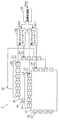
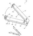
まず、実施の形態1に係る液晶表示装置1の概略構成について、図1を用いて説明する。図1は、実施の形態1に係る液晶表示装置の概略構成を模式的に示す図である。
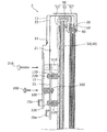
次に、実施の形態2に係る液晶表示装置2について、図13及び図14を用いて説明する。図13は、実施の形態2に係る液晶表示装置2の背面図である。図14は、図13のXIV−XIV線における同液晶表示装置2の部分断面図である。
以上、本開示に係る液晶表示装置について、実施の形態1、2に基づいて説明したが、本開示は、上記実施の形態1、2に限定されるものではない。
10 第1表示パネル
10a 第1液晶セル
10b 第1偏光板
11 第1ソースドライバ
12 第1ゲートドライバ
13 第1ソースFPC
14 第1ゲートFPC
15 第1回路基板
15a、43a 第1コネクタ
16 第1ケーブル
20 第2表示パネル
20a 第2液晶セル
20b 第2偏光板
21 第2ソースドライバ
22 第2ゲートドライバ
23 第2ソースFPC
24 第2ゲートFPC
25 第2回路基板
25a、43b 第2コネクタ
26 第2ケーブル
30 バックライト
31 光源
32 光学部材
32a 導光板
32b 反射シート
32c 拡散シート
41 第1タイミングコントローラ
42 第2タイミングコントローラ
43 画像処理部
50 フレーム
51 上フレーム
51a 第1ベゼル部
51b 第1側壁部
52 中フレーム
52a 第2ベゼル部
52b 第2側壁部
53 下フレーム
60 ホルダ
61 第1アーム部
61a、62a 第1面
61b、62b 第2面
62 第2アーム部
63 係止爪
64 係止穴
65 第1押さえ部
66 第1突起
67 第2突起
68 第2押さえ部
69 貫通孔
70 保護カバー
80、90 接合部材
100 スペーサボルト
110 第1スペーサボルト
120 第2スペーサボルト
200、210、220 ネジ
300 ナット
Claims (13)
- 第1液晶セルと、
第1フレキシブル配線基板を介して前記第1液晶セルに接続された第1回路基板と、
前記第1液晶セルに対向する第2液晶セルと、
第2フレキシブル配線基板を介して前記第2液晶セルに接続された第2回路基板と、
前記第2液晶セルを基準として前記第1液晶セルの反対側に配置されたフレームと、
前記第1回路基板及び前記第2回路基板を保持するホルダとを備え、
前記第1回路基板及び前記第2回路基板は、前記フレームを基準として前記第2液晶セルの反対側に配置され、
前記第2回路基板は、前記第1回路基板よりも前記フレームの近くに位置し、
前記ホルダは、前記第1回路基板を挟持し、前記第2回路基板を前記フレームと前記ホルダとの間に収納する、
液晶表示装置。 - 前記ホルダは、第1アーム部と、前記第1アーム部の長手方向の一端部及び他端部と連結される第2アーム部とを有し、
前記第1回路基板と前記第2回路基板との間に、前記第1アーム部又は前記第2アーム部が位置する、
請求項1に記載の液晶表示装置。 - 前記第1アーム部の前記一端部は、前記第2アーム部と着脱自在に前記第2アーム部に連結されており、
前記第1アーム部は、当該第1アーム部の前記他端部を回動支点として回動可能であり、
前記第1回路基板は、前記第1アーム部と前記第2アーム部との間で挟持され、
前記第2回路基板は、前記第2アーム部と前記フレームとの間の空間領域に配置されている、
請求項2に記載の液晶表示装置。 - 前記第1アーム部の前記一端部には、係止爪が設けられ、
前記第2アーム部には、前記係止爪が係止する係止体が設けられている、
請求項3に記載の液晶表示装置。 - 前記第2アーム部は、前記第1アーム部に対面する第1面と、前記第1面に対向し前記第1面よりも前記フレーム寄りに位置する第2面とを有し、
前記第1面には、前記第2アーム部の長手方向に間隔を空けて配置された一対の第1突起が設けられていて、
前記一対の第1突起の間に前記第1回路基板が配置されている、
請求項3又は4に記載の液晶表示装置。 - 前記第2面には、前記第2アーム部の長手方向に間隔を空けて配置された一対の第2突起が設けられており、
前記一対の第2突起の間に前記第2回路基板が配置されていて、
前記第2回路基板は、前記一対の第2突起と前記第2アーム部と前記フレームとで囲まれる空間領域に収容されている、
請求項5に記載の液晶表示装置。 - 前記第1アーム部は、前記第1回路基板の主面を前記第2アーム部側の方向に押さえ付ける第1押さえ部を有する、
請求項3〜6のいずれか1項に記載の液晶表示装置。 - 前記第2アーム部は、前記第2回路基板の主面を前記フレーム側の方向に押さえ付ける第2押さえ部を有する、
請求項3〜7のいずれか1項に記載の液晶表示装置。 - 前記液晶表示装置を背面視したときに、前記第1回路基板及び前記第2回路基板は、前記第2回路基板における前記第2フレキシブル配線基板が接続される第1端部とは反対側の第2端部が前記第1回路基板から露出するように配置されている、
請求項1〜8のいずれか1項に記載の液晶表示装置。 - 第1液晶セルと、
第1フレキシブル配線基板を介して前記第1液晶セルに接続された第1回路基板と、
前記第1液晶セルに対向する第2液晶セルと、
第2フレキシブル配線基板を介して前記第2液晶セルに接続された第2回路基板とを備え、
前記第1回路基板及び前記第2回路基板は、平面視の形状及び大きさが略同一であり、且つ、前記第2液晶セルの背面側に位置し、
前記第2回路基板は、前記第1回路基板よりも前記フレームの近くに位置し、
前記液晶表示装置を背面視したときに、前記第1回路基板及び前記第2回路基板は、前記第2回路基板における前記第2フレキシブル配線基板が接続される第1端部とは反対側の第2端部が前記第1回路基板から露出するように配置されている、
液晶表示装置。 - 前記液晶表示装置を背面視したときに、前記第2回路基板の全体が前記第1回路基板から露出している、
請求項10に記載の液晶表示装置。 - 前記第1回路基板と前記第2回路基板との間にスペーサボルトが配置され、
前記第1回路基板と前記スペーサボルトとはネジ又はナットによって固定されており、
前記第2回路基板と前記スペーサボルトとはナット又はネジによって固定されている、
請求項10に記載の液晶表示装置。 - さらに、前記第2液晶セルを基準として前記第1液晶セルの反対側に配置されたフレームを備え、
前記第1回路基板と前記フレームとの間に第1スペーサボルトが配置され、
前記第2回路基板と前記フレームとの間に第2スペーサボルトが配置され、
前記第1スペーサボルトの高さは、前記第2スペーサボルトの高さよりも高い、
請求項10〜12のいずれか1項に記載の液晶表示装置。
Priority Applications (5)
| Application Number | Priority Date | Filing Date | Title |
|---|---|---|---|
| JP2018122560A JP6882232B2 (ja) | 2018-06-28 | 2018-06-28 | 液晶表示装置 |
| US16/444,812 US10845635B2 (en) | 2018-06-28 | 2019-06-18 | Liquid crystal display device |
| US17/076,702 US11209684B2 (en) | 2018-06-28 | 2020-10-21 | Liquid crystal display device |
| JP2021078500A JP2021121868A (ja) | 2018-06-28 | 2021-05-06 | 液晶表示装置 |
| US17/456,331 US11579479B2 (en) | 2018-06-28 | 2021-11-23 | Liquid crystal display device |
Applications Claiming Priority (1)
| Application Number | Priority Date | Filing Date | Title |
|---|---|---|---|
| JP2018122560A JP6882232B2 (ja) | 2018-06-28 | 2018-06-28 | 液晶表示装置 |
Related Child Applications (1)
| Application Number | Title | Priority Date | Filing Date |
|---|---|---|---|
| JP2021078500A Division JP2021121868A (ja) | 2018-06-28 | 2021-05-06 | 液晶表示装置 |
Publications (2)
| Publication Number | Publication Date |
|---|---|
| JP2020003627A true JP2020003627A (ja) | 2020-01-09 |
| JP6882232B2 JP6882232B2 (ja) | 2021-06-02 |
Family
ID=69008051
Family Applications (2)
| Application Number | Title | Priority Date | Filing Date |
|---|---|---|---|
| JP2018122560A Active JP6882232B2 (ja) | 2018-06-28 | 2018-06-28 | 液晶表示装置 |
| JP2021078500A Pending JP2021121868A (ja) | 2018-06-28 | 2021-05-06 | 液晶表示装置 |
Family Applications After (1)
| Application Number | Title | Priority Date | Filing Date |
|---|---|---|---|
| JP2021078500A Pending JP2021121868A (ja) | 2018-06-28 | 2021-05-06 | 液晶表示装置 |
Country Status (2)
| Country | Link |
|---|---|
| US (3) | US10845635B2 (ja) |
| JP (2) | JP6882232B2 (ja) |
Families Citing this family (8)
| Publication number | Priority date | Publication date | Assignee | Title |
|---|---|---|---|---|
| US11287703B2 (en) * | 2019-06-12 | 2022-03-29 | Hisense Visual Technology Co., Ltd. | Dual-cell display device |
| CN111627935B (zh) * | 2020-06-09 | 2023-02-28 | 厦门天马微电子有限公司 | 一种显示面板及显示装置 |
| CN114093248A (zh) * | 2020-07-31 | 2022-02-25 | 京东方科技集团股份有限公司 | 拼接显示单元、拼接显示装置及其制作方法 |
| DE112020007145T5 (de) * | 2020-10-30 | 2023-03-02 | Boe Technology Group Co., Ltd. | Anzeigemodul |
| JP2023039701A (ja) * | 2021-09-09 | 2023-03-22 | 株式会社ジャパンディスプレイ | 表示装置 |
| US11694876B2 (en) | 2021-12-08 | 2023-07-04 | Applied Materials, Inc. | Apparatus and method for delivering a plurality of waveform signals during plasma processing |
| CN114624930B (zh) | 2022-03-29 | 2023-08-01 | 武汉华星光电技术有限公司 | 显示面板 |
| TWI832687B (zh) * | 2023-01-30 | 2024-02-11 | 友達光電股份有限公司 | 側面電路結構及其製造方法 |
Citations (7)
| Publication number | Priority date | Publication date | Assignee | Title |
|---|---|---|---|---|
| JPS63147890U (ja) * | 1987-03-19 | 1988-09-29 | ||
| JPH03106776U (ja) * | 1990-02-19 | 1991-11-05 | ||
| JPH08153981A (ja) * | 1994-11-25 | 1996-06-11 | Yaskawa Electric Corp | 基板固定構造 |
| JP3027084U (ja) * | 1996-01-22 | 1996-07-30 | 株式会社廣杉計器 | 金属薄板ねじ込取付用スペーサ |
| JP2012047838A (ja) * | 2010-08-25 | 2012-03-08 | Funai Electric Co Ltd | 液晶モジュールのx−プリント回路基板の固定構造 |
| US20150177527A1 (en) * | 2013-12-19 | 2015-06-25 | Samsung Electronics Co., Ltd. | Apparatus for displaying three-dimensional image |
| JP2018092172A (ja) * | 2016-12-05 | 2018-06-14 | 三星ディスプレイ株式會社Samsung Display Co.,Ltd. | 表示装置 |
Family Cites Families (17)
| Publication number | Priority date | Publication date | Assignee | Title |
|---|---|---|---|---|
| JPH114088A (ja) * | 1997-06-12 | 1999-01-06 | Nec Eng Ltd | ガイド付きサポート |
| JP2004327494A (ja) * | 2003-04-21 | 2004-11-18 | Fujitsu I-Network Systems Ltd | 装置筐体に実装したプリント回路板上への部品取付構造 |
| WO2007040127A1 (ja) | 2005-09-30 | 2007-04-12 | Sharp Kabushiki Kaisha | 液晶表示装置およびテレビジョン受信機 |
| US8451201B2 (en) * | 2005-09-30 | 2013-05-28 | Sharp Kabushiki Kaisha | Liquid crystal display device drive method, liquid crystal display device, and television receiver |
| JP4360405B2 (ja) * | 2007-01-05 | 2009-11-11 | エプソンイメージングデバイス株式会社 | 電気光学装置及び電子機器 |
| JP2012078546A (ja) * | 2010-10-01 | 2012-04-19 | Sharp Corp | 薄型表示装置 |
| JP5148775B1 (ja) * | 2012-01-13 | 2013-02-20 | シャープ株式会社 | 表示装置およびテレビジョン受像機 |
| JP5693624B2 (ja) * | 2012-03-19 | 2015-04-01 | キヤノン株式会社 | 表示装置 |
| DE202013012602U1 (de) | 2012-06-29 | 2017-12-22 | Saturn Licensing Llc | Anzeigeeinheit |
| DE102014222951B4 (de) * | 2014-11-11 | 2016-07-28 | Würth Elektronik eiSos Gmbh & Co. KG | Befestigungselement zur Befestigung an einer Leiterplatte sowie Befestigungsvorrichtung und Verfahren zum beabstandeten Verbinden von Leiterplatten mit einem derartigen Befestigungselement |
| KR102415651B1 (ko) * | 2015-07-01 | 2022-07-01 | 엘지전자 주식회사 | 이동 단말기 |
| JP6531033B2 (ja) * | 2015-11-24 | 2019-06-12 | 株式会社ジャパンディスプレイ | 表示装置 |
| JP6872863B2 (ja) * | 2016-07-13 | 2021-05-19 | パナソニック液晶ディスプレイ株式会社 | 表示装置 |
| KR20180063945A (ko) * | 2016-12-02 | 2018-06-14 | 삼성디스플레이 주식회사 | 실드 케이스 및 이를 구비하는 표시 장치 |
| JP6938188B2 (ja) * | 2017-03-27 | 2021-09-22 | パナソニック液晶ディスプレイ株式会社 | 表示装置 |
| US10306753B1 (en) * | 2018-02-22 | 2019-05-28 | International Business Machines Corporation | Enclosure-to-board interface with tamper-detect circuit(s) |
| US11122682B2 (en) * | 2018-04-04 | 2021-09-14 | International Business Machines Corporation | Tamper-respondent sensors with liquid crystal polymer layers |
-
2018
- 2018-06-28 JP JP2018122560A patent/JP6882232B2/ja active Active
-
2019
- 2019-06-18 US US16/444,812 patent/US10845635B2/en active Active
-
2020
- 2020-10-21 US US17/076,702 patent/US11209684B2/en active Active
-
2021
- 2021-05-06 JP JP2021078500A patent/JP2021121868A/ja active Pending
- 2021-11-23 US US17/456,331 patent/US11579479B2/en active Active
Patent Citations (7)
| Publication number | Priority date | Publication date | Assignee | Title |
|---|---|---|---|---|
| JPS63147890U (ja) * | 1987-03-19 | 1988-09-29 | ||
| JPH03106776U (ja) * | 1990-02-19 | 1991-11-05 | ||
| JPH08153981A (ja) * | 1994-11-25 | 1996-06-11 | Yaskawa Electric Corp | 基板固定構造 |
| JP3027084U (ja) * | 1996-01-22 | 1996-07-30 | 株式会社廣杉計器 | 金属薄板ねじ込取付用スペーサ |
| JP2012047838A (ja) * | 2010-08-25 | 2012-03-08 | Funai Electric Co Ltd | 液晶モジュールのx−プリント回路基板の固定構造 |
| US20150177527A1 (en) * | 2013-12-19 | 2015-06-25 | Samsung Electronics Co., Ltd. | Apparatus for displaying three-dimensional image |
| JP2018092172A (ja) * | 2016-12-05 | 2018-06-14 | 三星ディスプレイ株式會社Samsung Display Co.,Ltd. | 表示装置 |
Also Published As
| Publication number | Publication date |
|---|---|
| JP2021121868A (ja) | 2021-08-26 |
| US11579479B2 (en) | 2023-02-14 |
| US20220082880A1 (en) | 2022-03-17 |
| US20210041742A1 (en) | 2021-02-11 |
| US20200004078A1 (en) | 2020-01-02 |
| JP6882232B2 (ja) | 2021-06-02 |
| US10845635B2 (en) | 2020-11-24 |
| US11209684B2 (en) | 2021-12-28 |
Similar Documents
| Publication | Publication Date | Title |
|---|---|---|
| US11579479B2 (en) | Liquid crystal display device | |
| US11340484B2 (en) | Display device with flexible substrates | |
| US8780580B2 (en) | Display device | |
| US8237883B2 (en) | Liquid crystal display device | |
| CN101510018A (zh) | 液晶显示装置 | |
| CN100378515C (zh) | 用于lcd模块的面板模块 | |
| CN107664863B (zh) | 液晶显示装置 | |
| JP2020134848A (ja) | 液晶表示装置 | |
| KR101675838B1 (ko) | 액정표시장치 | |
| CN107123386A (zh) | 面板部和包括该面板部的显示设备 | |
| US10705364B2 (en) | Image display apparatus | |
| JP2007298699A (ja) | 液晶モジュール | |
| JP2011059339A (ja) | 液晶表示装置 | |
| JP2020122925A (ja) | 表示装置 | |
| JP7037455B2 (ja) | 表示装置、及びテレビ受信装置 | |
| WO2010055722A1 (ja) | 表示装置およびテレビ受信装置 | |
| JP2006317821A (ja) | 液晶表示装置 | |
| KR102377462B1 (ko) | 백라이트 유닛 및 이를 포함하는 액정 표시 장치 | |
| KR20050000952A (ko) | 액정표시장치 | |
| KR20000050959A (ko) | 엘씨디 구동 소자가 탑재된 에프피씨 및 이 에프피씨가 설치된 액정표시장치 | |
| KR20070035269A (ko) | 액정 표시 장치 | |
| JP2007065487A (ja) | 表示パネルの静電気防止装置 | |
| WO2013018746A1 (ja) | 表示パネル及びこれを備えた表示装置 |
Legal Events
| Date | Code | Title | Description |
|---|---|---|---|
| A621 | Written request for application examination |
Free format text: JAPANESE INTERMEDIATE CODE: A621 Effective date: 20191204 |
|
| A711 | Notification of change in applicant |
Free format text: JAPANESE INTERMEDIATE CODE: A711 Effective date: 20200501 |
|
| A977 | Report on retrieval |
Free format text: JAPANESE INTERMEDIATE CODE: A971007 Effective date: 20201007 |
|
| A131 | Notification of reasons for refusal |
Free format text: JAPANESE INTERMEDIATE CODE: A131 Effective date: 20201020 |
|
| A521 | Request for written amendment filed |
Free format text: JAPANESE INTERMEDIATE CODE: A523 Effective date: 20201216 |
|
| TRDD | Decision of grant or rejection written | ||
| A01 | Written decision to grant a patent or to grant a registration (utility model) |
Free format text: JAPANESE INTERMEDIATE CODE: A01 Effective date: 20210406 |
|
| A61 | First payment of annual fees (during grant procedure) |
Free format text: JAPANESE INTERMEDIATE CODE: A61 Effective date: 20210506 |
|
| R150 | Certificate of patent or registration of utility model |
Ref document number: 6882232 Country of ref document: JP Free format text: JAPANESE INTERMEDIATE CODE: R150 |
|
| S111 | Request for change of ownership or part of ownership |
Free format text: JAPANESE INTERMEDIATE CODE: R313117 |
|
| R350 | Written notification of registration of transfer |
Free format text: JAPANESE INTERMEDIATE CODE: R350 |
|
| R250 | Receipt of annual fees |
Free format text: JAPANESE INTERMEDIATE CODE: R250 |
|
| R250 | Receipt of annual fees |
Free format text: JAPANESE INTERMEDIATE CODE: R250 |