JP2020004705A - Display device - Google Patents
Display device Download PDFInfo
- Publication number
- JP2020004705A JP2020004705A JP2019068430A JP2019068430A JP2020004705A JP 2020004705 A JP2020004705 A JP 2020004705A JP 2019068430 A JP2019068430 A JP 2019068430A JP 2019068430 A JP2019068430 A JP 2019068430A JP 2020004705 A JP2020004705 A JP 2020004705A
- Authority
- JP
- Japan
- Prior art keywords
- layer
- groove
- substrate
- inorganic
- sealing layer
- Prior art date
- Legal status (The legal status is an assumption and is not a legal conclusion. Google has not performed a legal analysis and makes no representation as to the accuracy of the status listed.)
- Granted
Links
Images




Classifications
-
- H—ELECTRICITY
- H10—SEMICONDUCTOR DEVICES; ELECTRIC SOLID-STATE DEVICES NOT OTHERWISE PROVIDED FOR
- H10K—ORGANIC ELECTRIC SOLID-STATE DEVICES
- H10K59/00—Integrated devices, or assemblies of multiple devices, comprising at least one organic light-emitting element covered by group H10K50/00
- H10K59/60—OLEDs integrated with inorganic light-sensitive elements, e.g. with inorganic solar cells or inorganic photodiodes
-
- H—ELECTRICITY
- H10—SEMICONDUCTOR DEVICES; ELECTRIC SOLID-STATE DEVICES NOT OTHERWISE PROVIDED FOR
- H10K—ORGANIC ELECTRIC SOLID-STATE DEVICES
- H10K59/00—Integrated devices, or assemblies of multiple devices, comprising at least one organic light-emitting element covered by group H10K50/00
- H10K59/80—Constructional details
- H10K59/87—Passivation; Containers; Encapsulations
- H10K59/873—Encapsulations
-
- H—ELECTRICITY
- H10—SEMICONDUCTOR DEVICES; ELECTRIC SOLID-STATE DEVICES NOT OTHERWISE PROVIDED FOR
- H10K—ORGANIC ELECTRIC SOLID-STATE DEVICES
- H10K50/00—Organic light-emitting devices
- H10K50/80—Constructional details
- H10K50/84—Passivation; Containers; Encapsulations
-
- H—ELECTRICITY
- H10—SEMICONDUCTOR DEVICES; ELECTRIC SOLID-STATE DEVICES NOT OTHERWISE PROVIDED FOR
- H10K—ORGANIC ELECTRIC SOLID-STATE DEVICES
- H10K50/00—Organic light-emitting devices
- H10K50/80—Constructional details
- H10K50/84—Passivation; Containers; Encapsulations
- H10K50/842—Containers
- H10K50/8426—Peripheral sealing arrangements, e.g. adhesives, sealants
-
- H—ELECTRICITY
- H10—SEMICONDUCTOR DEVICES; ELECTRIC SOLID-STATE DEVICES NOT OTHERWISE PROVIDED FOR
- H10K—ORGANIC ELECTRIC SOLID-STATE DEVICES
- H10K50/00—Organic light-emitting devices
- H10K50/80—Constructional details
- H10K50/84—Passivation; Containers; Encapsulations
- H10K50/844—Encapsulations
-
- H—ELECTRICITY
- H10—SEMICONDUCTOR DEVICES; ELECTRIC SOLID-STATE DEVICES NOT OTHERWISE PROVIDED FOR
- H10K—ORGANIC ELECTRIC SOLID-STATE DEVICES
- H10K59/00—Integrated devices, or assemblies of multiple devices, comprising at least one organic light-emitting element covered by group H10K50/00
- H10K59/10—OLED displays
- H10K59/12—Active-matrix OLED [AMOLED] displays
-
- H—ELECTRICITY
- H10—SEMICONDUCTOR DEVICES; ELECTRIC SOLID-STATE DEVICES NOT OTHERWISE PROVIDED FOR
- H10K—ORGANIC ELECTRIC SOLID-STATE DEVICES
- H10K59/00—Integrated devices, or assemblies of multiple devices, comprising at least one organic light-emitting element covered by group H10K50/00
- H10K59/10—OLED displays
- H10K59/12—Active-matrix OLED [AMOLED] displays
- H10K59/124—Insulating layers formed between TFT elements and OLED elements
-
- H—ELECTRICITY
- H10—SEMICONDUCTOR DEVICES; ELECTRIC SOLID-STATE DEVICES NOT OTHERWISE PROVIDED FOR
- H10K—ORGANIC ELECTRIC SOLID-STATE DEVICES
- H10K59/00—Integrated devices, or assemblies of multiple devices, comprising at least one organic light-emitting element covered by group H10K50/00
- H10K59/10—OLED displays
- H10K59/12—Active-matrix OLED [AMOLED] displays
- H10K59/131—Interconnections, e.g. wiring lines or terminals
-
- H—ELECTRICITY
- H10—SEMICONDUCTOR DEVICES; ELECTRIC SOLID-STATE DEVICES NOT OTHERWISE PROVIDED FOR
- H10K—ORGANIC ELECTRIC SOLID-STATE DEVICES
- H10K59/00—Integrated devices, or assemblies of multiple devices, comprising at least one organic light-emitting element covered by group H10K50/00
- H10K59/80—Constructional details
- H10K59/87—Passivation; Containers; Encapsulations
-
- H—ELECTRICITY
- H10—SEMICONDUCTOR DEVICES; ELECTRIC SOLID-STATE DEVICES NOT OTHERWISE PROVIDED FOR
- H10K—ORGANIC ELECTRIC SOLID-STATE DEVICES
- H10K59/00—Integrated devices, or assemblies of multiple devices, comprising at least one organic light-emitting element covered by group H10K50/00
- H10K59/80—Constructional details
- H10K59/87—Passivation; Containers; Encapsulations
- H10K59/871—Self-supporting sealing arrangements
- H10K59/8722—Peripheral sealing arrangements, e.g. adhesives, sealants
-
- H—ELECTRICITY
- H10—SEMICONDUCTOR DEVICES; ELECTRIC SOLID-STATE DEVICES NOT OTHERWISE PROVIDED FOR
- H10K—ORGANIC ELECTRIC SOLID-STATE DEVICES
- H10K59/00—Integrated devices, or assemblies of multiple devices, comprising at least one organic light-emitting element covered by group H10K50/00
- H10K59/80—Constructional details
- H10K59/87—Passivation; Containers; Encapsulations
- H10K59/873—Encapsulations
- H10K59/8731—Encapsulations multilayered coatings having a repetitive structure, e.g. having multiple organic-inorganic bilayers
-
- H—ELECTRICITY
- H10—SEMICONDUCTOR DEVICES; ELECTRIC SOLID-STATE DEVICES NOT OTHERWISE PROVIDED FOR
- H10K—ORGANIC ELECTRIC SOLID-STATE DEVICES
- H10K77/00—Constructional details of devices covered by this subclass and not covered by groups H10K10/80, H10K30/80, H10K50/80 or H10K59/80
- H10K77/10—Substrates, e.g. flexible substrates
-
- Y—GENERAL TAGGING OF NEW TECHNOLOGICAL DEVELOPMENTS; GENERAL TAGGING OF CROSS-SECTIONAL TECHNOLOGIES SPANNING OVER SEVERAL SECTIONS OF THE IPC; TECHNICAL SUBJECTS COVERED BY FORMER USPC CROSS-REFERENCE ART COLLECTIONS [XRACs] AND DIGESTS
- Y02—TECHNOLOGIES OR APPLICATIONS FOR MITIGATION OR ADAPTATION AGAINST CLIMATE CHANGE
- Y02E—REDUCTION OF GREENHOUSE GAS [GHG] EMISSIONS, RELATED TO ENERGY GENERATION, TRANSMISSION OR DISTRIBUTION
- Y02E10/00—Energy generation through renewable energy sources
- Y02E10/50—Photovoltaic [PV] energy
- Y02E10/549—Organic PV cells
Landscapes
- Engineering & Computer Science (AREA)
- Microelectronics & Electronic Packaging (AREA)
- Physics & Mathematics (AREA)
- Optics & Photonics (AREA)
- Chemical & Material Sciences (AREA)
- Inorganic Chemistry (AREA)
- Life Sciences & Earth Sciences (AREA)
- Sustainable Development (AREA)
- Electroluminescent Light Sources (AREA)
- Devices For Indicating Variable Information By Combining Individual Elements (AREA)
Abstract
【課題】ディスプレイ装置を提供する。【解決手段】基板、基板上の回路層、回路層上のディスプレイ層、基板の表示領域内に位置して、基板、回路層及びディスプレイ層を貫通する少なくとも1つのホール、並びにホールを取り囲み、いずれもアンダーカット構造を有する少なくとも2つの溝を含み、該基板は、下方からのこの順に積層された第1基板、第1無機層、第2基板及び第2無機層を含み、少なくとも2つの溝は、いずれも、ディスプレイ層から第2基板までにわたって深さ方向に延長されたディスプレイ装置である。【選択図】図1A display device is provided. A substrate, a circuit layer on the substrate, a display layer on the circuit layer, at least one hole located in a display area of the substrate, penetrating the substrate, the circuit layer and the display layer, and surrounding the hole. Also includes at least two grooves having an undercut structure, the substrate includes a first substrate, a first inorganic layer, a second substrate, and a second inorganic layer stacked in this order from below, and the at least two grooves are Are display devices extending in the depth direction from the display layer to the second substrate. [Selection diagram] Fig. 1
Description
本発明は、ディスプレイ装置に関する。 The present invention relates to a display device.
最近、ディスプレイ装置の前面に、物理的ボタンなどが除去され、画面を表示するディスプレイ領域が拡大されており、該ディスプレイ領域を拡張させるために、カメラのようなディスプレイ装置機能のための別途の部材をディスプレイ領域内に配置させたディスプレイ装置が紹介されている。 Recently, physical buttons and the like have been removed from the front of the display device, and a display area for displaying a screen has been enlarged. In order to extend the display area, a separate member for a display device function such as a camera has been provided. Is introduced in the display area.
ここで、カメラといった別途の部材をディスプレイ領域内に配置するためには、ディスプレイ領域内に別途の部材が位置することができる凹部(recess)、溝(groove)または貫通部(through hole)などを形成する必要がある。しかし、該ディスプレイ領域内に形成された凹部、溝または貫通部は、外部の水分などがディスプレイ領域内に浸透する新たな透湿経路になってしまう。 Here, in order to dispose a separate member such as a camera in the display area, a recess (recess), a groove (groove) or a through hole (through hole) or the like, in which the separate member can be located in the display area, is provided. Need to be formed. However, the concave portion, the groove, or the penetrating portion formed in the display area becomes a new moisture-permeable path through which external moisture or the like penetrates into the display area.
本発明が解決しようとする課題は、ディスプレイ領域を最大化させながら、ディスプレイ領域内の貫通部を通じた、外部の水分などの浸透を効果的に遮断するディスプレイ装置を提供することである。 SUMMARY OF THE INVENTION It is an object of the present invention to provide a display device that effectively blocks external moisture and the like from penetrating through the display area while maximizing the display area.
本発明の一側面によるディスプレイ装置は、基板;前記基板上の回路層;前記回路層上のディスプレイ層;前記基板の表示領域内に位置して、前記基板、前記回路層及び前記ディスプレイ層を貫通する少なくとも1つのホール;及び、前記ホールを取り囲み、いずれもアンダーカット構造を有する少なくとも2つの溝を含み、前記基板は、下方からこの順に積層された第1基板、第1無機層、第2基板及び第2無機層を含み、前記少なくとも2つの溝は、いずれも、前記ディスプレイ層から前記第2基板までにわたって深さ方向に延長されうる。 A display device according to an aspect of the present invention includes: a substrate; a circuit layer on the substrate; a display layer on the circuit layer; a display layer on the circuit layer, which penetrates the substrate, the circuit layer, and the display layer. At least one hole; and at least two grooves surrounding the hole, each having an undercut structure, wherein the substrate is a first substrate, a first inorganic layer, and a second substrate stacked in this order from below. And at least two grooves may be extended in a depth direction from the display layer to the second substrate.
本実施形態において、前記少なくとも2つの溝は、前記ホールと最も近接し、前記ホールと離隔された第1溝と、前記第1溝を取り囲み、前記第1溝と離隔された第2溝と、を含み、前記第1無機層は、前記アンダーカット構造をなすように互いに対向して、前記第1溝内に突き出すように延長された1対の第1チップを含み、前記第1無機層は、前記アンダーカット構造をなすように互いに対向して、前記第2溝内に突き出すように延長された1対の第2チップを含んでもよい。 In this embodiment, the at least two grooves are closest to the hole, a first groove separated from the hole, a second groove surrounding the first groove and separated from the first groove, Wherein the first inorganic layer includes a pair of first chips which are opposed to each other so as to form the undercut structure and are extended so as to protrude into the first groove. And a pair of second chips extended to protrude into the second groove, facing each other to form the undercut structure.
本実施形態において、前記第2チップにおける、前記ホールに近い内側のものと、外側のものとを、部分的に連結するブリッジをさらに含み、前記ブリッジは、前記1対の第2チップと一体であり、前記第1チップは、前記ホールに近い内側のものと、外側のものとが、前記第1溝に沿った全体にわたって互いに離隔されうる。 In the present embodiment, the second chip further includes a bridge that partially connects an inner one near the hole and an outer one near the hole, wherein the bridge is integrated with the pair of second chips. The first chip may be separated from an inner chip near the hole and an outer chip along the first groove.
本実施形態において、前記ディスプレイ層を覆う封止層をさらに含み、前記封止層は、下方からこの順に積層された第1無機封止層、有機封止層及び第2無機封止層を含み、前記第1無機封止層は、前記第1溝及び前記第2溝の底面と内部の側壁面とを覆うことができる。 In this embodiment, the display device further includes a sealing layer covering the display layer, and the sealing layer includes a first inorganic sealing layer, an organic sealing layer, and a second inorganic sealing layer stacked in this order from below. The first inorganic sealing layer may cover a bottom surface and an inner side wall surface of the first groove and the second groove.
本実施形態において、前記第1無機封止層は、前記ブリッジの下面を覆うことができる。 In this embodiment, the first inorganic sealing layer can cover a lower surface of the bridge.
本実施形態において、前記有機封止層は、前記第2溝に充填されうる。 In this embodiment, the organic sealing layer may be filled in the second groove.
本実施形態において、前記第2無機封止層は、前記第1溝内において、前記第1無機封止層と接することができる。 In the present embodiment, the second inorganic sealing layer can be in contact with the first inorganic sealing layer in the first groove.
本実施形態において、前記第1無機封止層と前記第2無機封止層は、前記ホールの内部の側壁面にまで延長され、前記基板の側面と接することができる。 In the exemplary embodiment, the first inorganic sealing layer and the second inorganic sealing layer may extend to a side wall surface inside the hole and contact a side surface of the substrate.
本実施形態において、前記回路層は、薄膜トランジスタを含み、前記ディスプレイ層は、前記薄膜トランジスタと電気的に連結された有機発光素子を含んでもよい。 In this embodiment, the circuit layer may include a thin film transistor, and the display layer may include an organic light emitting device electrically connected to the thin film transistor.
本発明の他の側面によるディスプレイ装置は、下方からこの順に積層された第1基板、第1無機層、第2基板及び第2無機層を含む基板;前記基板上の回路層;前記回路層上のディスプレイ層;前記基板の表示領域内に位置して、前記基板、前記回路層及び前記ディスプレイ層を貫通する少なくとも1つのホール;前記基板の表示領域内に位置し、前記ホールを取り囲む第1溝及び第2溝;並びに、前記ディスプレイ層を覆う封止層;を含み、前記第2溝は、前記第1溝と離隔されて、前記第1溝を取り囲み、前記封止層の有機封止層は、前記第2溝を充填することができる。 A display device according to another aspect of the present invention includes a substrate including a first substrate, a first inorganic layer, a second substrate, and a second inorganic layer stacked in this order from below; a circuit layer on the substrate; At least one hole located in the display area of the substrate and penetrating the substrate, the circuit layer and the display layer; a first groove located in the display area of the substrate and surrounding the hole And a second groove; and a sealing layer covering the display layer; wherein the second groove is spaced from the first groove, surrounds the first groove, and is an organic sealing layer of the sealing layer. Can fill the second groove.
本実施形態において、前記第1溝及び前記第2溝は、いずれも、前記ディスプレイ層から前記第2基板までにわたって深さ方向に延長されうる。 In this embodiment, both the first groove and the second groove may extend in a depth direction from the display layer to the second substrate.
本実施形態において、前記封止層は、前記有機封止層の下方及び上方に、それぞれ第1無機封止層と第2無機封止層とをさらに含み、前記第1無機封止層と前記第2無機封止層は、前記第1溝内で互いに重ね合わされて接することができる。 In this embodiment, the sealing layer further includes a first inorganic sealing layer and a second inorganic sealing layer below and above the organic sealing layer, respectively, and the first inorganic sealing layer and the The second inorganic sealing layers may be overlapped and contact each other in the first groove.
本実施形態において、前記第1無機層は、前記ホールに近い内側と、外側とから、互いへと向かって、前記第1溝内に突き出すように延長された1対の第1チップを含み、前記第1無機層は、前記ホールに近い内側と、外側とから、互いへと向かって、前記第2溝内に突き出すように延長された1対の第2チップを含んでもよい。 In the present embodiment, the first inorganic layer includes a pair of first chips extended so as to protrude into the first groove from inside and outside near the hole and toward each other, The first inorganic layer may include a pair of second chips extended so as to protrude into the second groove from inside and outside near the hole toward each other.
本実施形態において、前記第1溝及び前記第2溝は、いずれも、上部での幅が、下部での幅よりも狭いのでありうる。 In this embodiment, the first groove and the second groove may each have a width at an upper portion smaller than a width at a lower portion.
本実施形態において、前記第1無機層は、前記第2溝に沿って配列されて、前記第2チップにおける、前記ホールに近い内側のものと、外側のものとを、部分的に互いに連結するブリッジをさらに含み、前記第1チップは、前記ホールに近い内側のものと、外側のものとが、前記第1溝に沿った全体にわたって互いに離隔されうる。 In the present embodiment, the first inorganic layer is arranged along the second groove, and partially connects the inside and the outside of the second chip near the hole to each other. The first chip may further include a bridge inside and near the hole, and the first chip may be separated from each other along the first groove.
本実施形態において、前記第1無機層は、前記ブリッジを複数個含み、複数個の前記ブリッジは、前記第2溝に沿って互いに一定の間隔で離隔されうる。 In the exemplary embodiment, the first inorganic layer includes a plurality of the bridges, and the plurality of the bridges may be separated from each other at a predetermined interval along the second groove.
本実施形態において、前記回路層は、薄膜トランジスタを含み、前記ディスプレイ層は、前記薄膜トランジスタと電気的に連結された有機発光素子を含んでもよい。 In this embodiment, the circuit layer may include a thin film transistor, and the display layer may include an organic light emitting device electrically connected to the thin film transistor.
本発明のさらに他の側面によるディスプレイ装置は、下方からこの順に積層された第1基板、第1無機層、第2基板及び第2無機層を含む基板;前記基板上の回路層;前記回路層上のディスプレイ層;前記基板の表示領域内に位置し、前記基板、前記回路層及び前記ディスプレイ層を貫通する少なくとも1つのホール;及び前記基板の表示領域内にて、前記ホールを取り囲む第1溝及び第2溝;を含み、前記第2無機層は、前記ホールに近い内側と、外側とから、互いへと向かって、前記第1溝内に突き出すように延長された1対の第1チップを含み、前記第2無機層は、互いへと向かって、前記第2溝内に突き出すように延長された1対の第2チップを含んでもよい。 A display device according to still another aspect of the present invention includes a substrate including a first substrate, a first inorganic layer, a second substrate, and a second inorganic layer stacked in this order from below; a circuit layer on the substrate; An upper display layer; at least one hole located in the display area of the substrate and penetrating the substrate, the circuit layer, and the display layer; and a first groove surrounding the hole in the display area of the substrate. And a second groove; wherein the second inorganic layer has a pair of first chips extending so as to protrude into the first groove from inside and outside near the hole toward each other. And the second inorganic layer may include a pair of second chips extended to project into the second groove toward each other.
本実施形態において、前記第1溝及び前記第2溝は、いずれも、前記ディスプレイ層から前記第2基板までにわたって深さ方向に延長され、前記第2溝は、前記第1溝と離隔され、前記第1溝を取り囲むことができる。 In this embodiment, both the first groove and the second groove extend in a depth direction from the display layer to the second substrate, and the second groove is separated from the first groove, The first groove may be surrounded.
本実施形態において、前記ディスプレイ層を覆う封止層をさらに含み、前記封止層は、前記第2溝を充填する有機封止層、並びに前記有機封止層の下方と上方とにそれぞれ位置する第1無機封止層及び第2無機封止層を含み、前記第1無機封止層と前記第2無機封止層とは、前記第1溝内にて、互いに重ね合わされて接することができる。 In this embodiment, the display device further includes a sealing layer covering the display layer, wherein the sealing layer is located below and above the organic sealing layer filling the second groove, and the organic sealing layer, respectively. The first inorganic sealing layer includes a first inorganic sealing layer and a second inorganic sealing layer, and the first inorganic sealing layer and the second inorganic sealing layer can be overlapped and contact with each other in the first groove. .
前述のところ以外の他の側面、特徴、利点は、下記の図面、特許請求の範囲、及び発明の詳細な説明から明確になるであろう。 Other aspects, features, and advantages other than those described above will become apparent from the following drawings, claims, and detailed description.
本発明によれば、カメラといった別途の部材が配置される貫通部を取り囲む複数の溝が形成されることで、貫通部を通じての外部の水分などの浸透を遮断することができる。 According to the present invention, by forming a plurality of grooves surrounding a through portion where a separate member such as a camera is arranged, it is possible to block penetration of external moisture and the like through the through portion.
また、少なくとも一つの溝においては、その上端の開口の縁部をなすように、互いに対向する1対のチップ部(内側のチップ部、及び外側のチップ部)が形成されるとともに、これらチップ部がブリッジによって部分的に互いに連結されることにより、チップ部の機械的強度が向上し、封止層の損傷を防止することができる。 Further, in at least one groove, a pair of chip portions (an inner chip portion and an outer chip portion) facing each other are formed so as to form an edge of an opening at an upper end thereof, and these chip portions are formed. Are partially connected to each other by the bridge, the mechanical strength of the chip portion is improved, and damage to the sealing layer can be prevented.
ここで、そのような効果により、本発明の範囲が限定されるものではないということは言うまでもない。 Here, it goes without saying that the scope of the present invention is not limited by such effects.
本発明は、多様な変換を加えることができ、さまざまな実施形態を有することができるが、特定の実施形態を図面に例示し、詳細な説明によって詳細に説明する。本発明の効果、特徴、及びそれらを達成する方法は、図面と共に詳細に説明する実施形態を参照すれば明確になるであろう。しかし、本発明は、以下で開示される実施形態に限定されるものではなく、多様な形態に具現されうるのである。 While the invention is capable of various modifications and various embodiments, certain embodiments are illustrated in the drawings and will be described in detail by the detailed description. The advantages, features and methods of achieving the present invention will become apparent with reference to the embodiments described in detail in conjunction with the drawings. However, the present invention is not limited to the embodiments disclosed below, but can be embodied in various forms.
以下の実施形態において、第1、第2といった用語は、限定的な意味ではなく、1つの構成要素を他の構成要素と区別する目的に使用された。 In the following embodiments, the terms first and second are not used in a limiting sense and are used for distinguishing one component from another.
以下の実施形態において、単数の表現は、文脈上明白に単数であることを意味しない限り、複数の表現を含む。 In the following embodiments, singular expressions include plural expressions unless the context clearly indicates otherwise.
以下の実施形態において、「含む」または「有する」といった用語は、明細書に記載された特徴または構成要素が存在するということを意味するものであり、1以上の他の特徴または構成要素が付加される可能性をあらかじめ排除するものではない。 In the following embodiments, the term “comprising” or “having” means that a feature or component described in the specification exists, and one or more other features or components may be added. It does not exclude the possibility of being done in advance.
以下の実施形態において、膜、領域、構成要素などの部分が、他の部分の上または上部にあるとするとき、他の部分のすぐ上にある場合だけではなく、その中間に、他の膜、領域、構成要素などが介在されている場合も含む。 In the following embodiments, when a part such as a film, a region, or a component is located on or above another part, not only when the part is directly above the other part but also in the middle of the other part, , Regions, components and the like are included.
図面においては、説明の便宜のために、構成要素がその大きさが誇張されていたり縮小されていたりする。例えば、図面に示された各構成の大きさ及び厚みは、説明の便宜のために任意に示されているので、本発明は、必ずしも図示されたところに限定されるものではない。 In the drawings, the size of components may be exaggerated or reduced for convenience of description. For example, the size and thickness of each component shown in the drawings are arbitrarily shown for convenience of description, and thus the present invention is not necessarily limited to the illustrated one.
ある実施形態が異なって具現可能である場合、特定の工程の順序は、説明される順序と異なるようにも遂行されうる。例えば、連続して説明される2つの工程が、実質的に同時に遂行されてもよく、説明される順序とは反対の順序に進められてもよい。 If an embodiment can be embodied differently, the order of the particular steps may be performed differently from the order described. For example, two steps described in succession may be performed substantially simultaneously, or may be performed in the reverse order to that described.
以下、添付された図面を参照し、本発明の実施形態について詳細に説明するが、図面を参照して説明するとき、同一であるか、あるいは対応する構成要素は、同一の図面符号を付す。 Hereinafter, embodiments of the present invention will be described in detail with reference to the accompanying drawings. In the description with reference to the drawings, the same or corresponding components are denoted by the same reference numerals.
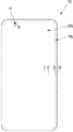
図1は、本発明の一実施形態によるディスプレイ装置の一例を概略的に図示した平面図であり、図2は、図1のI−I’に沿って切断した一例を概略的に図示した断面図である。 FIG. 1 is a plan view schematically illustrating an example of a display apparatus according to an embodiment of the present invention, and FIG. 2 is a cross-sectional view schematically illustrating an example taken along line II ′ of FIG. FIG.
本発明の一実施形態によるディスプレイ装置10は、基板100と、基板100上に、薄膜トランジスタ210などの回路素子を具備する回路層CLと、回路層CL上に、ディスプレイ素子310を含むディスプレイ層300と、を含んでもよい。一方、本発明で回路層CLは、薄膜トランジスタ210、キャパシタといった回路素子を含むだけではなく、薄膜トランジスタ210の内部及びその上に形成された各種絶縁層をいずれも含むことを意味する。言い換えれば、基板100の上面から平坦化層140までを回路層CLと定義することができる。同様に、ディスプレイ層300には、ディスプレイ素子310とともに、画素区画形成膜150までも含まれる。
The
本発明の一実施形態によるディスプレイ装置10は、複数個の画素が位置するディスプレイ領域AAと、ディスプレイ領域AAの外側に位置する周辺領域PAと、を有する。このことは、基板100が、そのようなディスプレイ領域AA及び周辺領域PAを有するというふうにも理解されうる。周辺領域PAは、各種電子素子や印刷回路基板などが電気的に接続される領域であるパッド領域を含んでもよい。
The
基板100のディスプレイ領域AAには、ディスプレイ素子310以外にも、ディスプレイ素子310と電気的に連結される薄膜トランジスタ210も位置することができる。図2においては、ディスプレイ素子310として、有機発光素子が、ディスプレイ領域AAに位置するように図示されている。そのような有機発光素子が薄膜トランジスタ210に電気的に連結されるということは、画素電極311が薄膜トランジスタ210に電気的に連結されることであると理解されうる。
In the display area AA of the
また、ディスプレイ領域AAには、少なくとも1つの貫通部Hが位置することができる。貫通部Hは、基板100、回路層CL及びディスプレイ層300を垂直方向に貫通する領域であり、それは、ディスプレイ装置10の機能のための別途の部材、またはディスプレイ装置10に新たな機能を追加させることができる別途の部材のための空間になりうる。例えば、ディスプレイ領域AAには、複数個の貫通部Hが形成され、貫通部Hには、センサ、光源、カメラモジュールなどが装着されうる。一方、貫通部Hは、基板100、回路層CL及びディスプレイ層300を貫通するので、外部の水分または酸素が、貫通部Hによって露出されたディスプレイ装置10の垂直の断面を通じて、ディスプレイ装置10の内部に浸透してしまう。しかし、本発明によれば、貫通部Hを取り囲む複数個の溝がさらに形成されるので、前述のような透湿を効果的に防止することができる。それについては、図4以下で詳細に説明することにし、以下では、図2を参照し、回路層CLとディスプレイ層300とについて、まず説明する。
Further, at least one penetration portion H can be located in the display area AA. The penetrating portion H is a region vertically penetrating the
基板100は、多様な素材を含んでもよい。画面が、基板100側に具現される背面発光型である場合、基板100は、透明な材質によって形成されなければならない。しかし、画面が基板100の反対側に具現される前面発光型である場合、基板100は、必ずしも透明な材質によって形成される必要はない。その場合、金属で基板100を形成することができる。金属で基板100を形成する場合、基板100は、鉄、クロム、マンガン、ニッケル、チタン、モリブデン、ステンレススチール(SUS)、インバー(invar)合金、インコネル(Inconel)合金、コバール(Kovar)合金などを含んでもよい。
The
基板100上には、バッファ層110が形成される。バッファ層110は、基板100上部に平坦面を提供することができ、基板100を通じて浸透する異物または湿気を、遮断することができる。例えば、バッファ層110は、シリコン酸化物、シリコン窒化物、シリコン酸窒化物、アルミニウム酸化物、アルミニウム窒化物、チタン酸化物またはチタン窒化物などの無機物や、ポリイミド、ポリエステル、アクリルなどの有機物を含みうるのであり、例示した材料のうちの複数のものによる積層体としても形成されうる。
On the
このように、バッファ層110は基板100の上面に接触することができる。また、このバッファ層110は、周辺領域PAにまでわたって、基板100の全面に形成されうる。
As such, the
基板100上には、薄膜トランジスタ210、及び薄膜トランジスタ210と電気的に連結された表示素子310が位置することができる。
A
薄膜トランジスタ210は、活性層211、ゲート電極213、ソース電極215a及びドレイン電極215bを含んでもよい。以下では、薄膜トランジスタ210が、活性層211、ゲート電極213、ソース電極215a及びドレイン電極215bが、下方からこの順に形成されたトップゲートタイプ(top gate type)である場合について説明する。しかし、本実施形態は、それに限定されるものではなく、ボトムゲートタイプ(bottom gate type)といった多様なタイプの薄膜トランジスタ210が採用されてもよい。
The
活性層211は、非晶質シリコン(amorphous silicon)または多結晶シリコン(polycrystalline silicon)といった半導体物質を含んでもよい。しかし、本実施形態は、それに限定されるものではなく、活性層211は、多様な物質を含んでもよい。任意選択的な実施形態として、活性層211は、有機半導体物質などを含んでもよい。さらに他の選択的実施形態として、活性層211は、酸化物半導体物質を含んでもよい。例えば、活性層211は、亜鉛(Zn)、インジウム(In)、ガリウム(Ga)、スズ(Sn)カドミウム(Cd)、ゲルマニウム(Ge)のような12,13,14族金属元素、及びそれらの組み合わせのうちから選択された物質の酸化物を含んでもよい。
The
ゲート絶縁膜121は、活性層211上に形成される。ゲート絶縁膜121は、シリコン酸化物及び/またはシリコン窒化物などの無機物質からなる積層膜または単層膜として形成されうる。ゲート絶縁膜121は、活性層211とゲート電極213とを絶縁する役割を行う。ゲート絶縁膜121は、表示領域AAだけではなく、周辺領域PAまで延長されて形成されうる。
The
ゲート電極213は、ゲート絶縁膜121の上部に形成される。ゲート電極213は、薄膜トランジスタ210にオン/オフ信号を印加するゲートライン(図示せず)と連結されうる。
The
ゲート電極213は、低抵抗の金属物質からなるのでありうる。例えば、ゲート電極213は、アルミニウム(Al)、白金(Pt)、パラジウム(Pd)、銀(Ag)、マグネシウム(Mg)、金(Au)、ニッケル(Ni)、ネオジム(Nd)、イリジウム(Ir)、クロム(Cr)、リチウム(Li)、カルシウム(Ca)、モリブデン(Mo)、チタン(Ti)、タングステン(W)、銅(Cu)のうちの1つ以上の物質による積層膜または単層膜として形成されうる。
The
ゲート電極213上には、層間絶縁膜131が形成される。層間絶縁膜131は、ソース電極215a及びドレイン電極215bと、ゲート電極213とを絶縁させる。層間絶縁膜131は、表示領域AAだけではなく、周辺領域PAにまで延長されて形成されうる。
On the
層間絶縁膜131は、無機物質からなる積層膜または単層膜として形成されうる。例えば、該無機物質は、金属酸化物または金属窒化物でもあり、具体的には、該無機物質は、シリコン酸化物(SiO2)、シリコン窒化物(SiNx)、シリコン酸窒化物(SiON)、アルミニウム酸化物(Al2O3)、チタン酸化物(TiO2)、タンタル酸化物(Ta2O5)、ハフニウム酸化物(HfO2)または亜鉛酸化物(ZrO2)などを含んでもよい。
The
層間絶縁膜131上には、ソース電極215a及びドレイン電極215bを形成することができる。ソース電極215a及びドレイン電極215bは、活性層211の領域と接触するように形成される。ソース電極215a及びドレイン電極215bは、アルミニウム(Al)、白金(Pt)、パラジウム(Pd)、銀(Ag)、マグネシウム(Mg)、金(Au)、ニッケル(Ni)、ネオジム(Nd)、イリジウム(Ir)、クロム(Cr)、リチウム(Li)、カルシウム(Ca)、モリブデン(Mo)、チタン(Ti)、タングステン(W)、銅(Cu)のうちの1つ以上の物質による積層膜または単層膜として形成されうる。例えば、ソース電極215a及びドレイン電極215bは、チタン(Ti)によるベース保護層、アルミニウム(Al)の層及びチタン(Ti)によるキャッピング層の3層積層構造を有することができる。
A
ソース電極215a上及びドレイン電極215b上には、平坦化層140が形成される。平坦化層140は、薄膜トランジスタ210による段差を解消し、下方の面の凹凸により、ディスプレイ素子310に不良が発生することを防止する。平坦化層140は、有機物質からなる積層膜または単層膜として形成されうる。有機物質は、PMMA(polymethylmethacrylate)やPS(polystylene)といった一般の汎用高分子、フェノール系基を有する高分子誘導体、アクリル系高分子、イミド系高分子、アリールエーテル系高分子、アミド系高分子、フッ素系高分子、p−キシレン系高分子、ビニルアルコール系高分子、及びそれらのブレンドなどを含んでもよい。また、平坦化層140は、無機絶縁膜と有機絶縁膜との複合積層体によっても形成されうる。
A
平坦化層140上には、ディスプレイ素子310が形成される。ディスプレイ素子310は、一例として、第1電極311、第1電極311と対向する第2電極315、及び、第1電極311と第2電極315との間に介在される中間層313を具備した有機発光素子でありうる。
The
第1電極311は、平坦化層140上に形成され、薄膜トランジスタ210と電気的に連結されうる。第1電極311は、多様な形態を有することができるが、例えば、フォトリソグラフィ法により、アイランド状にパターニングされて形成されうる。
The
第1電極311の一例として、反射電極でありうる。例えば、第1電極311は、Ag、Mg、Al、Pt、Pd、Au、Ni、Nd、Ir、Cr、及びそれらの化合物などによって形成された反射膜と、反射膜上に形成された透明または半透明の電極層と、を具備することができる。透明または半透明の電極層は、酸化スズインジウム(ITO)、酸化亜鉛インジウム(IZO)、酸化スズ亜鉛インジウム(ITZO)、酸化ガリウム亜鉛(GZO)及び酸化ガリウム亜鉛インジウム(IGZO)を含むグループのうちから選択された少なくとも1つ以上を具備することができる。
An example of the
一例として、第1電極311は、透明または半透明の電極層である第1導電層、銀を含む第2導電層、及び透明または半透明の電極層である第3導電層の積層構造を有することができる。また、銀を含む第2導電層は、銀の凝集現象を防止するために、銀と同一であるか、あるいはそれより小さい原子半径を有する合金元素をさらに含んでもよい。該合金元素は、亜鉛(Zn)、ニッケル(Ni)、コバルト(Co)、銅(Cu)、ガリウム(Ga)、ゲルマニウム(Ge)、白金(Pt)、アンチモン(Sb)、マンガン(Mn)、タングステン(W)及びモリブデン(Mo)のうちの少なくともいずれか一つを含んでもよい。
For example, the
第2電極315は、透明または半透明の電極でありうるのであり、Li、Ca、LiF/Ca、LiF/Al、Al、Ag、Mg、及びそれらの化合物を含む、仕事関数が小さい金属薄膜によって形成されうる。また、金属薄膜の上に、ITO、IZO、ZnOまたはIn2O3のような透明電極形成用物質でもって、補助電極層やバス電極をさらに形成することができる。従って、第2電極315は、中間層313に含まれた有機発光層から放出された光を透過させることができる。すなわち、有機発光層から放出される光は、直接に、または、反射電極で構成された第1電極311によって反射されて、第2電極315の側に放出されうる。
The
しかし、本実施形態のディスプレイ装置10は、前面発光型に制限されるものではなく、有機発光層から放出された光が、基板100側に放出される背面発光型であることもありうる。その場合、第1電極311は、透明または半透明の電極によって構成されうるのであり、第2電極315は、反射電極によって構成されうる。また、本実施形態のディスプレイ装置10は、前面及び背面の両方向に光を放出する両面発光型であることもありうる。
However, the
一方、第1電極311上には、絶縁物により、画素区画形成膜150が形成される。画素区画形成膜150は、ポリイミド、ポリアミド、アクリル樹脂、ベンゾシクロブテン樹脂及びフェノール樹脂からなる群から選択される1以上の有機絶縁物質により、スピンコーティングなどの方法によって形成されうる。画素区画形成膜150は、第1電極311の所定領域を露出させ、露出された領域に、有機発光層を含む中間層313が位置する。すなわち、画素区画形成膜150は、有機発光素子の画素領域(画素開口)を区画形成する。
On the other hand, the pixel
中間層313に含まれた有機発光層は、低分子有機物または高分子有機物でありうるのであり、中間層313は、有機発光層以外に、ホール輸送層(HTL:hole transport layer)、ホール注入層(HIL:hole injection layer)、電子輸送層(ETL:electron transport layer)及び電子注入層(EIL:electron injection layer)といった機能層を選択的にさらに含んでもよい。
The organic light emitting layer included in the
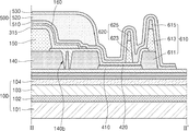
図3は、図1のII−II’に沿って切断した一例を概略的に図示した断面図である。図3においては、図2で説明していない周辺領域PA(図1)や、ディスプレイ層300(図2)上に配置された封止層500などについて説明し、基板100の構成について、さらに詳細に説明する。
FIG. 3 is a cross-sectional view schematically illustrating an example taken along the line II-II 'of FIG. In FIG. 3, the peripheral area PA (FIG. 1) not described in FIG. 2 and the
まず、基板100は、下方からこの順に積層された第1基板101、第1無機層102、第2基板103及び第2無機層104を含んでもよい。
First, the
第1基板101と第2基板103は、例えば、SiO2を主成分にする透明なガラス材質からなりうる。しかし、第1基板101と第2基板103は、必ずしもそれに限定されるものではなく、透明なプラスチック材質によっても形成されうる。該プラスチック材質は、ポリエーテルスルホン(PES)、ポリアクリレート(PAR)、ポリエーテルイミド(PEI)、ポリエチレンナフタレート(PEN)、ポリエチレンテレフタレート(PET)、ポリフェニレンスルフィド(PPS)、ポリアリレート(polyallylate)、ポリイミド(polyimide)、ポリカーボネート(PC)、セルローストリアセテート(TAC)、セルロースアセテートプロピオネート(CAP)などでありうる。
The
第1基板101と第2基板103は、互いに同一の厚み、あるいは相異なる厚みを有することができる。例えば、第1基板101と第2基板103は、いずれも、ポリイミドを含み、3μmないし20μmの厚みを有するのでありうる。
The
第1無機層102と第2無機層104は、外部からの異物の浸透を防止するバリア層であり、窒化ケイ素(SiNx)及び/または酸化ケイ素(SiOx)といった無機物を含む単層膜または積層膜でありうる。第1無機層102と第2無機層104は、いずれも、4,000Åないし7,000Åの厚みを有することができるが、本発明は、それに限定されるものではない。
The first
ディスプレイ装置10(図1)は、ディスプレイ層300(図2)を覆い、外部の水分や酸素などからディスプレイ素子310(図2)を保護するための封止層500を含み、周辺領域PA(図1)には、第2電極315と電気的に接続された電極電源供給ライン410などが配置されうる。
The display device 10 (FIG. 1) includes a
電極電源供給ライン410は、ディスプレイ領域AA(図1)内の多様な導電層を形成する際に、同一の物質で同時に形成することができる。一例として、電極電源供給ライン410は、ソース電極215a(図2)及びドレイン電極215b(図2)の形成時に共に形成され、層間絶縁膜131上に位置することができる。ただし、本発明は、それに限定されるものではなく、電極電源供給ライン410は、ゲート電極213(図2)を形成する際に、ゲート絶縁膜121(図2)上に、同一の物質によって同時に形成されうるというように、多様な変形が可能である。
The electrode
電極電源供給ライン410は、第2電極315に直接コンタクトすることもできる。また、図3に図示されているように、保護導電層420を介して、第2電極315に電気的に連結されうる。すなわち、平坦化層140上に位置し、第2電極315と接続された保護導電層420が、電極電源供給ライン410上に延長され、電極電源供給ライン410に電気的に連結されうる。保護導電層420は、一例として、第1電極311(図2)を平坦化層140上に形成する際に、同一の物質によって同時に形成されうる。
The electrode
一方、外部からの酸素や水分などの不純物が、平坦化層140を介して、ディスプレイ領域AA(図1)内に浸透することを防止するため、図3に図示されているように、平坦化層140が、周辺領域PA(図1)中、ディスプレイ領域AAの縁に沿って延びる溝状の開口140bを有する。図示の具体例では、2本の溝状の開口140bが、互いに近接して並行に延びている。また、保護導電層420を形成する際に、保護導電層420が、溝状の開口140bを充填する。このことを通じて、周辺領域PA(図1)の平坦化層140に浸透した不純物が、ディスプレイ領域AA(図1)内の平坦化層140に浸透することを効果的に防止することができる。
On the other hand, to prevent impurities such as oxygen and moisture from the outside from penetrating into the display area AA (FIG. 1) through the
平坦化層140が有する溝状の開口140bは、多様な形状を有することができる。例えば、平坦化層140が有する溝状の開口140bは、ディスプレイ領域AA(図1)外側にて、そのエッジに沿って延び、ディスプレイ領域AA(図1)を切れ目なく取り囲むことができる。そして、ディスプレイ領域AA(図1)を切れ目なしに取り囲む溝状の開口140bを、複数個、互いに並行に配置されるようにして有することもできる。
The groove-shaped
なお、図示の例では、溝状の開口140bが、外側(基板の縁の側)のものと、内側(ディスプレイ領域AAの側)のものとの、二重に形成されており、これら2本の互いに並行に延びる溝により、さらに効果的に、不純物の浸透を防止することができる。
In the example shown in the figure, the groove-
第2電極315上には、有機発光素子で生じた光の効率を向上させる役割を行う、キャッピング層160が位置することができる。キャッピング層160は、第2電極315を覆うとともに、第2電極315の外縁を越える箇所にまで延長されて、キャッピング層160の端部が、平坦化層140の上面に、直接に、または、保護導電層420を介して接するように位置する。そのようなキャッピング層160は、有機物を含む。
On the
キャッピング層160の上方には、封止層500が位置する。封止層500は、外部からの水分や酸素などから、有機発光素子を保護する役割を行う。そのために、封止層500は、有機発光素子が位置するディスプレイ領域AA(図1)はもとより、ディスプレイ領域AA(図1)の外側の周辺領域PA(図1)にまで延長された形状を有する。そのような封止層500は、図3に図示されているように、積層構造を有することができる。具体的には、封止層500は、下方からこの順に積層された第1無機封止層510、有機封止層520及び第2無機封止層530を含んでもよい。
Above the
第1無機封止層510は、キャッピング層160を覆い、シリコン酸化物、シリコン窒化物及び/またはシリコン酸窒化物などを含んでもよい。そのような第1無機封止層510は、その下方の構造物の上面の起伏に沿って形成されうる。
The first
すなわち、第1無機封止層510は、高周波マグネトロンスパッタリングや、プラズマCVD法などにより、例えば、溝などの内面も全体を覆うように形成することができる。特に、化学気相蒸着法(CVD)法により形成する場合、チップの上面、側面及び底面と溝の側面及び底面にわたって、切れず連続的に成膜することができる。
That is, the first
有機封止層520は、第1無機封止層510を覆い、十分な厚みを有し、有機封止層520の上面は、実質的に平坦でありうる。そのような有機封止層520は、ポリエチレンテレフタレート、ポリエチレンナフタレート、ポリカーボネート、ポリイミド、ポリエチレンスルホネート、ポリオキシメチレン、ポリアリレート、ヘキサメチルジシロキサンからなる群から選択された1以上の材料を含んでもよい。
The
第2無機封止層530は、有機封止層520を覆い、シリコン酸化物、シリコン窒化物及び/またはシリコン酸窒化物などを含んでもよい。第1無機封止層510と第2無機封止層530の配置領域は、有機封止層520の配置領域より大きい面積を有し、有機封止層520の外縁の外側にて互いに接することができる。すなわち、第1無機封止層510と第2無機封止層530とにより、有機封止層520が外部に露出されないようにすることができる。
The second
そのように封止層500は、第1無機封止層510、有機封止層520及び第2無機封止層530を含むが、そのような多層構造を通じて、封止層500内にクラックが発生したとしても、第1無機封止層510と有機封止層520との間、または有機封止層520と第2無機封止層530との間で、そのようなクラックを連結させないようにすることができる。このことを通じて、外部からの水分や酸素などがディスプレイ領域AAに浸透するような経路の形成を防止したり最小化させたりすることができる。
As such, the
一方、そのような封止層500を形成する過程において、その下方の構造物が損傷されうる。例えば、第1無機封止層510は、化学気相蒸着法(CVD)を利用して形成されうるが、そのような化学気相蒸着法を利用して第1無機封止層510を形成する際、第1無機封止層510が形成されるその直下の層が損傷されうる。従って、第1無機封止層510をキャッピング層160上に直接形成することになれば、有機発光素子で生じた光の効率を向上させる役割を行うキャッピング層160が損傷され、ディスプレイ装置の光効率が低下してしまう。従って、封止層500を形成する過程において、キャッピング層160の損傷を防止するために、キャッピング層160と封止層500との間に保護層が介在されるようにすることができる。そのような保護層は、LiFを含んでもよい。
Meanwhile, in the process of forming the
なお、封止層500を形成する際、具体的には、有機封止層520を形成する際、有機封止層520形成用の物質が、事前に設定された領域内に位置するように限定することが必要である。そのために、図3に図示されているように、第1ダム610を周辺領域PA(図1)に位置させる。第1ダム610は、平坦化層140の外縁から離隔されるようにして、周辺領域PA(図1)内に位置する。
Note that when forming the
第1ダム610は、積層構造を有することができる。一例として、第1ダム610は、第1層611、第2層613及び第3層615が積層された構造を有することができる。第1層611は、平坦化層140を形成する際、これと同一の物質によって同時に形成されうるのであり、第2層613は、画素区画形成膜150を形成する際、これと同一の物質によって同時に形成されうる。第3層615は、第2層613と同一の物質によって、第2層613上に追加して形成することができる。
The
第1ダム610は、製造過程において、有機発光素子の中間層313(図2)や第2電極315を形成する際、またはその後のキャッピング層160を形成する際に、使用されるマスクを支持する役割を行うのであり、このようなマスクを用いた蒸着またはパターニングの過程にて、その前に形成された構成要素がマスクにコンタクトして損傷されることを防止することができる。また、第1ダム610は、第1無機封止層510上に有機封止層520を形成する際、有機封止層520形成用の物質を、基板100のエッジの側へと移動させない。それだけではなく、第1ダム610が平坦化層140と離隔されて位置することにより、外部からの水分が、有機物質からなる平坦化層140を伝って、ディスプレイ領域AA内に浸透することを防止することができる。
The
一方、封止層500の第1無機封止層510と、第2無機封止層530は、図3に図示されているように、第1ダム610を覆って第1ダム610の外側まで延長され、外部の水分及び酸素の浸透をさらに効果的に防止することができる。
Meanwhile, the first
第1ダム610の内側には、第2ダム620がさらに形成されうる。第2ダム620は、電極電源供給ライン410上の保護導電層420の上に位置することができる。第2ダム620は、第1ダム610の第2層613と同一の物質によって同時に形成されうる下層623と、下層623上に位置し、第1ダム610の第3層615と同一の物質によって同時に形成されうる上層625と、を含むことにより、すなわち、平坦化層140と同時に形成される第1層611を省くことにより、第1ダム610より低い高さを有することができる。
A
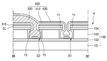
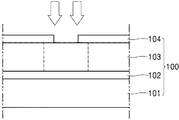
図4は、図1のA部分を拡大して概略的に図示した拡大図であり、図5は、図4のIII−III’の断面の一例を概略的に図示した断面図であり、図6は、図4のIV−IV’の断面の一例を概略的に図示した断面図であり、図7は、図4の溝を形成する方法を概略的に図示した断面図であり、図8は図4のIII−III’の断面の他の例を概略的に図示した断面図である。 FIG. 4 is an enlarged view schematically showing the portion A of FIG. 1 in an enlarged manner, and FIG. 5 is a sectional view schematically showing an example of a section taken along line III-III ′ of FIG. 6 is a cross-sectional view schematically illustrating an example of a cross-section taken along line IV-IV ′ of FIG. 4, FIG. 7 is a cross-sectional view schematically illustrating a method of forming the groove of FIG. FIG. 3 is a cross-sectional view schematically illustrating another example of the cross section taken along line III-III ′ of FIG. 4.
まず、図4ないし図6を参照すれば、ディスプレイ領域AA(図1)内に形成されたホールHは、基板100、回路層CL及びディスプレイ層300を貫通することができる。また、ホールHの周辺には、ホールHを取り囲む、少なくとも2つのリング状の溝G1,G2が形成されうる。少なくとも2つの溝G1,G2は、ディスプレイ層300から基板100の一部の領域まで延長されうる。以下においては、少なくとも2つの溝G1,G2のうち、ホールHに近い順序により、第1溝G1及び第2溝G2と命名する。すなわち、ホールHと最も近接して配置されたリング状の溝を第1溝G1とする。一方、図4においては、円形のホールHを取り囲む2つの円形リング状の溝G1,G2を例示しているが、本発明は、それに限られるものではなく、このようなリング状の溝は、3つ以上形成されてもよい。
First, referring to FIGS. 4 to 6, the holes H formed in the display area AA (FIG. 1) can penetrate the
また、ホールHの輪郭の形状は、楕円形、長円形、角を丸めた四角形などであってもよく、その場合、リング状の溝G1,G2も、ホールHの輪郭の形状と相似形またはこれに類似の形状することができる。 Further, the shape of the contour of the hole H may be elliptical, elliptical, square with rounded corners, or the like. In this case, the ring-shaped grooves G1 and G2 also have a shape similar to the shape of the contour of the hole H or Similar shapes can be provided.
第1溝G1は、ホールHと離隔された位置にて、ホールHを取り囲むように形成される。第1溝G1は、アンダーカット構造を有することができる。例えば、第1溝G1は、ホールHから所定の距離だけ離間した箇所(リング状の領域)にて、第1基板101、第1無機層102、第2基板103及び第2無機層104がこの順に積層された基板100から、第2無機層104が省かれるとともに、第2基板103が、その厚みの少なくとも一部にまで除去されることで、形成されうる。ここで、第2無機層104は、第1溝G1における開放された上端部にて、互いに対向し互いに近づくように延長されて、板状に突き出す1対の第1チップ(tip)T1を含んでもよい。すなわち、第1溝G1は、開口の上端部での幅が、第1溝G1の内部または底での幅より狭いのでありうる。ここで、第1溝G1の幅は、第1溝G1が延びる方向と垂直の方向にて測定された距離を意味する。例えば、第1溝G1が円形である場合、第1溝G1の幅は、前記円の周方向と垂直の方向、すなわち、半径方向を意味する。
The first groove G1 is formed to surround the hole H at a position separated from the hole H. The first groove G1 may have an undercut structure. For example, the first groove G1 is formed such that the
1対の第1チップT1は、図7に図示される方法によって形成することができる。さらに具体的には、第2無機層104をパターニングして開口を形成した後、第2無機層104をマスクとして使用し、第2無機層104の上部において、第2基板103を除去するためのレーザを照射したり、乾式エッチングを進めたりすれば、第2基板103は、第2無機層104の開口より広く除去され、マスクとして使用された第2無機層104の開口パターンは、1対のチップT1を構成する。
The pair of first chips T1 can be formed by the method illustrated in FIG. More specifically, after patterning the second
ところが、上記のように、1対の第1チップT1が形成された基板100上に、ディスプレイ素子310を形成すれば、ディスプレイ素子310などと同時に形成されて第1溝G1の内部に残留する有機物層を含む積層膜(例えば、HTL, HIL, ETL, 及び/または EIL)は、第1溝G1の側壁面とは接触しない。すなわち、1対の第1チップT1によるアンダーカット構造により、第1溝G1の内部の側壁面に接触するようには形成されない。その結果、ディスプレイ素子310などと同時に形成される積層膜(例えば、HTL, HIL, ETL, 及び/または EIL)は、第2基板103とは不連続的に、第1溝G1の底の上面の一部にだけ形成される。従って、第1溝G1内にて、ディスプレイ素子310に含まれた各種有機層が断絶され、ホールHを介して流入された外部の水分または酸素が、ディスプレイ素子310の内部の各種有機層を伝って、ディスプレイ領域AA(図1)にまで浸透することを遮断することができる。
However, as described above, if the
第2溝G2は、第1溝G1と離隔された領域であり、第1溝G1を取り囲むように形成される。第2溝G2の基本的な構成は、第1溝G1と同一でありうる。すなわち、第2溝G2は、1対の第2チップT2を含み、アンダーカット構造を有し、開口端部での幅が、第2溝G2の下端部での幅より狭い。一方、第2溝G2の第2チップT2は、第1チップT1とは異なり、ホールHに近い内側のものと、外側のものとが、第2溝G2の長手方向(リング状の周方向)に沿った全領域にて互いに完全に離隔されるのではない。すなわち、第1チップT1は、第1溝G1の全体にわたって、ホールHに近い内側のものと、外側のものとが互いに離隔されたのであるが、第2チップT2は、内側のものと、外側のものとが、ブリッジBにより、部分的に互いに連結されうる。 The second groove G2 is a region separated from the first groove G1, and is formed so as to surround the first groove G1. The basic configuration of the second groove G2 can be the same as the first groove G1. That is, the second groove G2 includes a pair of second chips T2, has an undercut structure, and has a width at the opening end portion smaller than the width at the lower end portion of the second groove G2. On the other hand, the second chip T2 of the second groove G2 is different from the first chip T1 in that the inner chip near the hole H and the outer chip are located in the longitudinal direction (ring-shaped circumferential direction) of the second groove G2. Are not completely separated from each other in the entire area along. That is, in the first chip T1, the inner chip near the hole H and the outer chip are separated from each other over the entire first groove G1, while the second chip T2 is separated from the inner chip and the outer chip. Can be partially connected to each other by a bridge B.
ブリッジBは、第2チップT2を部分的に連結し、第2チップT2の機械的強度を向上させることができる。従って、第2チップT2に衝撃が加えられても、第2チップT2の損傷を防止し、封止層500の第1無機封止層510または第2無機封止層530にクラックが発生することを防止することができる。ブリッジBは、複数個が形成され、第2溝G2の長手方向に沿って等間隔で離隔されるか、あるいは不規則に離隔されるのでありうる。ブリッジBは、第2チップT2と一体に形成されうる。一方、第1溝G1は、ホールHと最も近接するように位置するので、第1チップT1が、ブリッジBによって連結された場合は、ブリッジB上にディスプレイ層300などが形成され、連続的な有機層が形成されうる。そのため、第1チップT1は、内側のものと、外側のものとが、第1溝G1の全体にわたって互いに離隔されなければならない。
The bridge B partially connects the second chip T2, and can improve the mechanical strength of the second chip T2. Therefore, even if an impact is applied to the second chip T2, damage to the second chip T2 is prevented, and cracks are generated in the first
一方、ディスプレイ素子310の積層膜などは、第1溝G1及び第2溝G2のアンダーカット構造により、第1溝G1や第2溝G2の内部の垂直壁面に接するようには形成されない。ところが、封止層500の第1無機封止層510は、第1溝G1の内面に沿ってコンフォーマルに形成されるようにすることができる。そのため、第1溝G1及び第2溝G2の内部の垂直壁面だけではなく、第1チップT1及び第2チップT2の下面にも形成されうる。すなわち、第1無機封止層510は、ホールHの縁にまで、断絶されずに連続的に形成されうる。
On the other hand, due to the undercut structure of the first groove G1 and the second groove G2, the laminated film and the like of the
第1無機封止層510は、図6に図示されているように、ブリッジBの下面にも形成されるようにすることができる。そのようにするために、ブリッジBの幅は、第2チップT2の突出寸法の2倍以下に形成されうる。ここで、ブリッジBの幅は、第2溝G2の長手方向(第2溝G2が延びる方向)に沿った寸法を意味し、第2チップT2の突出寸法は、ホールHに近い内側のものと、外側のものとが、それぞれ、第2溝G2の幅方向に沿って突き出す寸法を意味する。ブリッジBの幅は、第2チップT2の突出寸法の2倍以下に形成されれば、ブリッジBの下面にも、第1無機封止層510が形成されることを確保することができる。したがって、ブリッジBの下面にて、第1無機封止層510が部分的に断絶されることを防止することができる。
The first
一方、有機封止層520は、第2溝G2の内部を充填することができる。すなわち、有機封止層520を形成する際、有機封止層520形成用の物質は、第2溝G2の内部に充填されることで、第2溝G2の外側にあふれることが防止される。言い換えれば、第2溝G2は、有機封止層520が形成される領域と、形成されない領域とを区画する構造物として機能できるので、図3で説明した第1ダム610(図3)を省略することができる。また、それにより、ホールHの周辺の非表示領域を最小化させることができる。
Meanwhile, the
第2無機封止層530は、第1無機封止層510と同様に形成されうる。従って、第2無機封止層530と第1無機封止層510は、ホールHと最も近接した第1溝G1の内部にて、第2無機封止層530と第1無機封止層510とは、重なり合わされて互いに接し、外部の水分及び酸素の浸透を防止することができる。
The second
任意選択的な実施形態において、第1無機封止層510と第2無機封止層530とは、図8で図示するように、ホールHの内部の側壁面にまで延長され、基板100の側面と接することができる。特に、図示の具体例のように、ホールHの内部にあって、基板100の側面の全体を被覆することができる。従って、外部の水分及び酸素の浸透をさらに効果的に防止することができる。
In an optional embodiment, the first
以上、本発明は、図面に図示された一実施形態を参照して説明したが、それらは、例示的なものに過ぎず、当該分野において当業者であるならば、それらから多様な変形、及び実施形態の変形が可能であるという点を理解するであろう。従って、本発明の真の技術的保護範囲は、特許請求の範囲の技術的思想によって決められるものである。 Although the present invention has been described with reference to an embodiment illustrated in the drawings, it is only by way of example and, if one of ordinary skill in the art is a person skilled in the art, various modifications, and It will be appreciated that variations of the embodiments are possible. Therefore, the true technical protection scope of the present invention is determined by the technical idea of the appended claims.
より具体的な、好ましい一実施形態によると下記のとおりである。 According to a more specific and preferred embodiment:
近年、スマートホンやタブレットPCなどには、自撮り(selfie)用のカメラやフラッシュ光源またはセンサが、画像表示面側の周辺部に搭載されることが多い。従来は、矩形の画像表示面の外側、特には、表示パネルの外側に、カメラなどが配置されていた。 In recent years, smartphones, tablet PCs, and the like often have a camera for selfie, a flash light source, or a sensor mounted on a peripheral portion on the image display surface side. Conventionally, a camera or the like is arranged outside the rectangular image display surface, particularly, outside the display panel.
しかし、近年、携帯機器のサイズを大きくせずに画像表示面を極力大きくするために、画像表示面を取り囲む画像非表示の周縁部(額縁)を、極力狭くする(狭額縁化)ようになっている。 However, in recent years, in order to make the image display surface as large as possible without increasing the size of the portable device, the peripheral portion (frame) of the image non-display surrounding the image display surface is made as narrow as possible (narrower frame). ing.
表示パネルの周辺部を折り曲げることができる有機発光表示装置を用いる場合、駆動回路部を搭載した周辺部を、側面または裏面側へと折り曲げることで、画像非表示の周縁部(額縁)をなくすことも可能である。 In the case of using an organic light-emitting display device in which the peripheral portion of the display panel can be bent, the peripheral portion on which the drive circuit portion is mounted is bent to the side surface or the back surface side to eliminate the peripheral portion (frame) for non-image display. Is also possible.
このような場合、矩形の画像表示面に、ユーザーから向かって上端からの湾入部を設け、この中に、カメラやセンサを配置することが行なわれている。 In such a case, a rectangular image display surface is provided with an indentation from the upper end facing the user, and a camera and a sensor are arranged in the indentation.
しかし、この湾入部の分だけ、画像表示面が小さくなってしまう。また、表示パネルについて、折り曲げや折り畳み可能とする場合、湾入部があると、その近傍に応力が集中するおそれもある。 However, the image display surface is reduced by the size of the bay. Further, in the case where the display panel can be bent or folded, if there is an indentation, stress may be concentrated in the vicinity thereof.
そこで、極力小さくしたカメラを、画像表示面(矩形の画像表示領域)の内部にて、表示パネルに貫通孔(through hole)を開けて埋め込むようにすることが考えられる。画像表示面の上端に、タッチパネル式の選択ボタンなどを配置するならば、カメラを埋め込んでも違和感がないようにすることができる。 In view of this, it is conceivable that a camera whose size is reduced as much as possible is embedded in the display panel by opening a through hole in the image display surface (rectangular image display area). If a touch panel type selection button or the like is arranged at the upper end of the image display surface, it is possible to prevent a sense of incongruity even if the camera is embedded.
ところが、表示パネルに貫通孔を設けると、有機発光表示装置からなる表示パネルを用いる場合、貫通孔の箇所から、画素配列領域へと、有機層を伝って、水分や酸素が浸透するおそれがある。 However, when a through-hole is provided in the display panel, when a display panel including an organic light-emitting display device is used, moisture and oxygen may permeate through the organic layer from the location of the through-hole to the pixel array region. .
第2基板103の厚みは、3μmないし20μm、特には5μmないし15μmでありうる。また、第2無機層104の厚みは、4,000Åないし7,000Å(400〜700nm)または200〜800nm、例えば500〜600nmでありうる。第2無機層104は、スパッタリング法などにより形成することができる。第1無機封止層510及び第2無機封止層530の厚みは、第2無機層104の厚みと同様とすることができる。また、有機封止層520の厚みは、例えば1〜5μmとすることができる。
The thickness of the
ホールHの径は、例えば0.5mm〜2mmであり、ホールHと内側のリング溝(第1溝G1)との間の間隔、及びリング溝(第1溝G1及び第2溝G2)同士の間隔は、例えば、0.05〜0.3mmとすることができ、リング溝(第1溝G1及び第2溝G2)の幅は、例えば、10〜50μmとすることができる。また、オーバーハング部(一対の第2チップT2)の突出寸法は、例えば、リング溝(第1溝G1及び第2溝G2)の幅の10〜30%とすることができる。 The diameter of the hole H is, for example, 0.5 mm to 2 mm, and the distance between the hole H and the inner ring groove (the first groove G1) and the distance between the ring grooves (the first groove G1 and the second groove G2). Can be, for example, 0.05 to 0.3 mm, and the width of the ring groove (the first groove G1 and the second groove G2) can be, for example, 10 to 50 μm. In addition, the protrusion dimension of the overhang portion (the pair of second chips T2) can be, for example, 10 to 30% of the width of the ring groove (the first groove G1 and the second groove G2).
なお、ホール(貫通孔)Hが、周辺領域PAにほぼ接して設けられる場合、第1溝G1及び第2溝G2は、例えば、ホールHを、左右及び向かって下方の三方から取り囲む、U字型のものであっても良い。 When the hole (through-hole) H is provided substantially in contact with the peripheral area PA, the first groove G1 and the second groove G2 are, for example, U-shaped, which surround the hole H from the left, right, and downward from three directions. It may be of a type.
本発明のディスプレイ装置は、例えば、表示関連の技術分野に効果的に適用可能である。 The display device of the present invention can be effectively applied to, for example, display-related technical fields.
10 ディスプレイ装置
100 基盤
210 薄膜トランジスタ
300 ディスプレイ層
500 封止層
Claims (20)
前記基板上の回路層と、
前記回路層上のディスプレイ層と、
前記基板の表示領域内に位置して、前記基板、前記回路層及び前記ディスプレイ層を貫通する少なくとも1つのホールと、
前記ホールを取り囲み、いずれもアンダーカット構造を有する少なくとも2つの溝と、を含み、
前記基板は、下方からこの順に積層された第1基板、第1無機層、第2基板及び第2無機層を含み、
前記少なくとも2つの溝は、いずれも、前記ディスプレイ層から前記第2基板までにわたって深さ方向に延長されたディスプレイ装置。 Board and
A circuit layer on the substrate,
A display layer on the circuit layer;
At least one hole penetrating the substrate, the circuit layer and the display layer, located in a display area of the substrate;
At least two grooves surrounding the hole, each having an undercut structure;
The substrate includes a first substrate, a first inorganic layer, a second substrate, and a second inorganic layer stacked in this order from below,
The display device, wherein each of the at least two grooves extends in a depth direction from the display layer to the second substrate.
前記第1無機層は、前記アンダーカット構造をなすように互いに対向して、前記第1溝内に突き出すように延長された1対の第1チップを含み、
前記第1無機層は、前記アンダーカット構造をなすように互いに対向して、前記第2溝内に突き出すように延長された1対の第2チップを含むことを特徴とする請求項1に記載のディスプレイ装置。 The at least two grooves include a first groove closest to the hole and separated from the hole, and a second groove surrounding the first groove and separated from the first groove,
The first inorganic layer includes a pair of first chips that are opposed to each other so as to form the undercut structure and are extended to protrude into the first groove.
2. The first inorganic layer according to claim 1, wherein the first inorganic layer includes a pair of second chips that are opposed to each other so as to form the undercut structure and extend to protrude into the second groove. 3. Display device.
前記ブリッジは、前記1対の第2チップと一体であり、
前記第1チップは、前記ホールに近い内側のものと、外側のものとが、前記第1溝に沿った全体にわたって互いに離隔されたことを特徴とする請求項2に記載のディスプレイ装置。 The second chip further includes a bridge that partially connects the inner one near the hole and the outer one,
The bridge is integral with the pair of second chips;
3. The display device according to claim 2, wherein the first chip and an inner chip near the hole are separated from each other throughout the first groove. 4.
前記封止層は、下方からこの順に積層された第1無機封止層、有機封止層及び第2無機封止層を含み、
前記第1無機封止層は、前記第1溝及び前記第2溝の底面と内部の側壁面とを覆うことを特徴とする請求項3に記載のディスプレイ装置。 Further comprising a sealing layer covering the display layer,
The sealing layer includes a first inorganic sealing layer, an organic sealing layer, and a second inorganic sealing layer stacked in this order from below,
4. The display device of claim 3, wherein the first inorganic sealing layer covers a bottom surface of the first groove and the second groove and an inner side wall surface. 5.
前記基板上の回路層と、
前記回路層上のディスプレイ層と、
前記基板の表示領域内に位置して、前記基板、前記回路層及び前記ディスプレイ層を貫通する少なくとも1つのホールと、
前記基板の表示領域内に位置して、前記ホールを取り囲む第1溝及び第2溝と、
前記ディスプレイ層を覆う封止層と、を含み、
前記第2溝は、前記第1溝と離隔されて、前記第1溝を取り囲み、
前記封止層の有機封止層は、前記第2溝を充填するディスプレイ装置。 A substrate including a first substrate, a first inorganic layer, a second substrate, and a second inorganic layer sequentially stacked;
A circuit layer on the substrate,
A display layer on the circuit layer;
At least one hole penetrating the substrate, the circuit layer and the display layer, located in a display area of the substrate;
A first groove and a second groove which are located in a display area of the substrate and surround the hole;
A sealing layer covering the display layer,
The second groove is spaced apart from the first groove and surrounds the first groove;
The display device, wherein the organic sealing layer of the sealing layer fills the second groove.
前記第1無機封止層と前記第2無機封止層とは、前記第1溝内で互いに重ね合わされて接することを特徴とする請求項11に記載のディスプレイ装置。 The sealing layer further includes a first inorganic sealing layer and a second inorganic sealing layer below and above the organic sealing layer, respectively.
The display device according to claim 11, wherein the first inorganic sealing layer and the second inorganic sealing layer overlap each other and are in contact with each other in the first groove.
前記第1無機層は、前記ホールに近い内側と、外側とから、互いへと向かって、前記第2溝内に突き出すように延長された1対の第2チップを含むことを特徴とする請求項10に記載のディスプレイ装置。 The first inorganic layer includes a pair of first chips extended so as to protrude into the first groove from inside and outside close to the hole toward each other, from the outside.
The first inorganic layer includes a pair of second chips that extend from the inside and outside close to the hole toward each other and protrude into the second groove. Item 11. The display device according to item 10.
前記第1チップは、前記ホールに近い内側のものと、外側のものとが、前記第1溝に沿った全体にわたって互いに離隔されたことを特徴とする請求項13に記載のディスプレイ装置。 The first inorganic layer is further arranged along the second groove, and further includes a bridge that partially connects the inside of the second chip near the hole and the outside of the second chip to each other,
14. The display device according to claim 13, wherein the first chip and the inner chip near the hole are separated from each other throughout the first groove.
前記基板上の回路層と、
前記回路層上のディスプレイ層と、
前記基板の表示領域内に位置し、前記基板、前記回路層及び前記ディスプレイ層を貫通する少なくとも1つのホールと、
前記基板の表示領域内にて、前記ホールを取り囲む第1溝及び第2溝と、を含み、
前記第2無機層は、前記ホールに近い内側と、外側とから、互いへと向かって、前記第1溝内に突き出すように延長された1対の第1チップを含み、
前記第2無機層は、前記ホールに近い内側と、外側とから、互いへ向かって、前記第2溝内に突き出すように延長された1対の第2チップを含むディスプレイ装置。 A substrate including a first substrate, a first inorganic layer, a second substrate, and a second inorganic layer sequentially stacked;
A circuit layer on the substrate,
A display layer on the circuit layer;
At least one hole located in a display area of the substrate, penetrating the substrate, the circuit layer, and the display layer;
A first groove and a second groove surrounding the hole in a display area of the substrate,
The second inorganic layer includes a pair of first chips extended so as to protrude into the first groove from inside and outside close to the hole and toward each other,
The display device, wherein the second inorganic layer includes a pair of second chips extended so as to protrude into the second groove from inside and outside near the hole toward each other.
前記封止層は、前記第2溝を充填する有機封止層、並びに前記有機封止層の下方と上方とにそれぞれ位置する第1無機封止層及び第2無機封止層を含み、
前記第1無機封止層と前記第2無機封止層とは、前記第1溝内にて、互いに重ね合わされて接することを特徴とする請求項18に記載のディスプレイ装置。 Further comprising a sealing layer covering the display layer,
The sealing layer includes an organic sealing layer filling the second groove, and a first inorganic sealing layer and a second inorganic sealing layer located below and above the organic sealing layer, respectively.
19. The display device according to claim 18, wherein the first inorganic sealing layer and the second inorganic sealing layer are overlapped with each other and contact each other in the first groove.
Applications Claiming Priority (2)
| Application Number | Priority Date | Filing Date | Title |
|---|---|---|---|
| KR10-2018-0075579 | 2018-06-29 | ||
| KR1020180075579A KR102742881B1 (en) | 2018-06-29 | 2018-06-29 | Display device |
Publications (2)
| Publication Number | Publication Date |
|---|---|
| JP2020004705A true JP2020004705A (en) | 2020-01-09 |
| JP7301579B2 JP7301579B2 (en) | 2023-07-03 |
Family
ID=67180515
Family Applications (1)
| Application Number | Title | Priority Date | Filing Date |
|---|---|---|---|
| JP2019068430A Active JP7301579B2 (en) | 2018-06-29 | 2019-03-29 | display device |
Country Status (5)
| Country | Link |
|---|---|
| US (4) | US10930885B2 (en) |
| EP (1) | EP3588574B1 (en) |
| JP (1) | JP7301579B2 (en) |
| KR (2) | KR102742881B1 (en) |
| CN (2) | CN119343015A (en) |
Cited By (3)
| Publication number | Priority date | Publication date | Assignee | Title |
|---|---|---|---|---|
| WO2021205603A1 (en) * | 2020-04-09 | 2021-10-14 | シャープ株式会社 | Display device and method for manufacturing same |
| KR20220057434A (en) | 2020-10-29 | 2022-05-09 | 도쿄엘렉트론가부시키가이샤 | Organic el panel manufacturing method and organic el panel |
| WO2022224073A1 (en) * | 2021-04-23 | 2022-10-27 | 株式会社半導体エネルギー研究所 | Display device and method for manufacturing display device |
Families Citing this family (31)
| Publication number | Priority date | Publication date | Assignee | Title |
|---|---|---|---|---|
| KR20190108212A (en) | 2018-03-13 | 2019-09-24 | 삼성디스플레이 주식회사 | Display panel and method of manufacturing display apparatus including the same |
| KR102742881B1 (en) | 2018-06-29 | 2024-12-16 | 삼성디스플레이 주식회사 | Display device |
| KR102548987B1 (en) | 2018-08-09 | 2023-06-29 | 삼성디스플레이 주식회사 | Display device |
| KR102626939B1 (en) * | 2018-10-05 | 2024-01-19 | 삼성디스플레이 주식회사 | Display device |
| KR102653262B1 (en) | 2018-10-16 | 2024-04-01 | 삼성전자 주식회사 | apparatus having a touch layer with openings |
| CN110164916B (en) | 2018-12-05 | 2021-02-02 | 京东方科技集团股份有限公司 | Display panel, display apparatus, and method of manufacturing display panel |
| KR102168042B1 (en) * | 2018-12-27 | 2020-10-20 | 엘지디스플레이 주식회사 | Display Device |
| KR102800324B1 (en) | 2019-04-29 | 2025-04-29 | 삼성디스플레이 주식회사 | Electronic device |
| KR102721171B1 (en) * | 2019-06-21 | 2024-10-25 | 삼성디스플레이 주식회사 | Display apparatus |
| CN110335964B (en) * | 2019-06-26 | 2020-11-10 | 武汉华星光电半导体显示技术有限公司 | Display panel |
| KR102720609B1 (en) * | 2019-07-19 | 2024-10-24 | 삼성디스플레이 주식회사 | Flexible display device |
| CN110265583B (en) * | 2019-07-26 | 2022-08-12 | 京东方科技集团股份有限公司 | A display panel, method of making the same, and display device |
| CN110416434B (en) * | 2019-08-06 | 2022-01-28 | 京东方科技集团股份有限公司 | Display substrate, preparation method thereof and display device |
| CN110444690B (en) * | 2019-08-20 | 2022-03-04 | 京东方科技集团股份有限公司 | Display substrate, manufacturing method thereof and display device |
| CN111192974B (en) * | 2020-01-07 | 2022-07-12 | 武汉华星光电半导体显示技术有限公司 | Array substrate and preparation method thereof |
| CN111244322B (en) | 2020-01-17 | 2022-04-26 | 京东方科技集团股份有限公司 | Display substrate, manufacturing method thereof and display device |
| CN111627930B (en) * | 2020-05-27 | 2022-09-09 | 武汉华星光电半导体显示技术有限公司 | Array substrate and preparation method thereof, and display panel |
| KR102912630B1 (en) * | 2020-07-02 | 2026-01-14 | 삼성디스플레이 주식회사 | Display Panel and Method of manufacturing the same |
| CN111834546A (en) * | 2020-07-07 | 2020-10-27 | 武汉华星光电半导体显示技术有限公司 | Display device, display panel and manufacturing method thereof |
| US11600800B2 (en) * | 2020-07-31 | 2023-03-07 | Innolux Corporation | Electronic device having a curved profile interface corresponding to a recess |
| CN112599701B (en) * | 2020-12-14 | 2022-05-17 | 合肥维信诺科技有限公司 | Display substrate |
| CN112820742A (en) * | 2021-01-19 | 2021-05-18 | 合肥维信诺科技有限公司 | Preparation method of display panel and display panel |
| US12532643B2 (en) * | 2021-02-12 | 2026-01-20 | Sharp Kabushiki Kaisha | Display device |
| CN113193015B (en) * | 2021-04-16 | 2022-07-12 | 武汉华星光电技术有限公司 | Display panel, preparation method thereof and display device |
| CN113192983B (en) * | 2021-04-19 | 2022-12-06 | 武汉华星光电半导体显示技术有限公司 | Display panel and preparation method thereof |
| CN114613923A (en) * | 2022-03-14 | 2022-06-10 | 武汉华星光电半导体显示技术有限公司 | Display panel and display device |
| CN114649392A (en) * | 2022-03-15 | 2022-06-21 | 深圳市华星光电半导体显示技术有限公司 | Display panel and display device |
| US20230317633A1 (en) * | 2022-03-30 | 2023-10-05 | Win Semiconductors Corp. | Semiconductor chip |
| CN114824127B (en) * | 2022-04-06 | 2023-04-07 | 武汉华星光电半导体显示技术有限公司 | Display panel and manufacturing method thereof |
| CN115275037B (en) * | 2022-04-06 | 2025-07-25 | 武汉华星光电半导体显示技术有限公司 | Display panel and display device |
| CN115915843A (en) * | 2023-01-30 | 2023-04-04 | 武汉天马微电子有限公司 | Manufacturing method of display panel, display panel and display device |
Citations (6)
| Publication number | Priority date | Publication date | Assignee | Title |
|---|---|---|---|---|
| JP2011008969A (en) * | 2009-06-23 | 2011-01-13 | Canon Inc | Display |
| US20160190389A1 (en) * | 2014-12-26 | 2016-06-30 | Samsung Display Co., Ltd. | Display device and method of manufacturing the same |
| US20170031323A1 (en) * | 2015-07-29 | 2017-02-02 | Lg Display Co., Ltd. | Organic light emitting display device |
| US20170148856A1 (en) * | 2015-11-20 | 2017-05-25 | Samsung Display Co., Ltd | Organic light-emitting display and method of manufacturing the same |
| KR20170059864A (en) * | 2015-11-20 | 2017-05-31 | 삼성디스플레이 주식회사 | Organic light emitting display and manufacturing method using the same |
| US20180151834A1 (en) * | 2016-11-28 | 2018-05-31 | Japan Display Inc. | Display device |
Family Cites Families (40)
| Publication number | Priority date | Publication date | Assignee | Title |
|---|---|---|---|---|
| KR101137389B1 (en) * | 2009-12-15 | 2012-04-20 | 삼성모바일디스플레이주식회사 | Substrate for flexible display device, methode for manufacturing the same, and method for manufacturing organic light emitting device |
| KR101801913B1 (en) | 2012-03-23 | 2017-11-28 | 삼성디스플레이 주식회사 | Organic light emitting display device and the method for manufacturing the same |
| TWI637949B (en) | 2013-06-14 | 2018-10-11 | 塩野義製藥股份有限公司 | Aminotriazine derivative and pharmaceutical composition comprising the same |
| KR102262530B1 (en) | 2014-02-17 | 2021-06-09 | 엘지이노텍 주식회사 | Touch window and display with the same |
| WO2015170213A1 (en) | 2014-05-06 | 2015-11-12 | Semiconductor Energy Laboratory Co., Ltd. | Electronic device |
| KR102228857B1 (en) | 2014-09-05 | 2021-03-17 | 엘지전자 주식회사 | Protable electronic device |
| KR102391361B1 (en) * | 2015-01-14 | 2022-04-27 | 삼성디스플레이 주식회사 | Organic light emitting diode display |
| CN104714699A (en) | 2015-04-13 | 2015-06-17 | 京东方科技集团股份有限公司 | Flexible display device |
| KR102378758B1 (en) | 2015-06-19 | 2022-03-25 | 엘지디스플레이 주식회사 | Flexible display apparatus |
| KR20170015832A (en) | 2015-08-01 | 2017-02-09 | 이승범 | A Snow Remove Device |
| KR102370169B1 (en) | 2015-10-13 | 2022-03-04 | 엘지전자 주식회사 | Flexible display device and operating method thereof |
| KR102421579B1 (en) | 2015-11-16 | 2022-07-18 | 삼성디스플레이 주식회사 | Foldable display apparatus |
| EP3173855B1 (en) | 2015-11-27 | 2020-12-09 | LG Electronics Inc. | Rollable display device |
| KR20170069864A (en) | 2015-12-13 | 2017-06-21 | 배도연 | automatic liquidation ticket barrier |
| JP6646473B2 (en) | 2016-02-25 | 2020-02-14 | 株式会社ジャパンディスプレイ | Display device and method of manufacturing display device |
| KR101766352B1 (en) | 2016-03-10 | 2017-08-09 | (주)하드램 | Multi-wavelength selective laser cutting system for flexible device |
| KR102421577B1 (en) | 2016-04-05 | 2022-07-18 | 삼성디스플레이 주식회사 | Display device |
| KR102454386B1 (en) | 2016-04-29 | 2022-10-17 | 엘지디스플레이 주식회사 | Rollable flexible display device |
| KR102492731B1 (en) | 2016-06-09 | 2023-01-27 | 삼성디스플레이 주식회사 | Rollable display device |
| KR102605208B1 (en) | 2016-06-28 | 2023-11-24 | 삼성디스플레이 주식회사 | Organic light emitting display device and method of manufacturing an organic light emitting display device |
| KR102493527B1 (en) | 2016-07-05 | 2023-02-01 | 삼성디스플레이 주식회사 | Rollable display device and electronic device including the same |
| KR102537297B1 (en) | 2016-07-05 | 2023-05-30 | 삼성디스플레이 주식회사 | Rollable display device and electronic device including the same |
| CN109315032B (en) | 2016-07-21 | 2020-09-08 | 夏普株式会社 | Organic EL display device |
| KR102362096B1 (en) | 2017-05-29 | 2022-02-11 | 삼성디스플레이 주식회사 | Display device |
| WO2018229941A1 (en) | 2017-06-15 | 2018-12-20 | シャープ株式会社 | Display device |
| WO2019064488A1 (en) | 2017-09-29 | 2019-04-04 | シャープ株式会社 | Elastic support substrate for flexible display, flexible display, and flexible display laminate |
| KR102448325B1 (en) | 2017-11-16 | 2022-09-30 | 삼성디스플레이 주식회사 | Display panel and electronic device including same |
| EP3488962A1 (en) | 2017-11-28 | 2019-05-29 | Vestel Elektronik Sanayi ve Ticaret A.S. | Solder composition and method of soldering |
| KR102520016B1 (en) * | 2018-02-02 | 2023-04-11 | 삼성디스플레이 주식회사 | Display panel and electronic device having the same |
| KR102583898B1 (en) | 2018-04-30 | 2023-10-04 | 삼성디스플레이 주식회사 | Display panel and method of manufacturing the same |
| KR102742881B1 (en) * | 2018-06-29 | 2024-12-16 | 삼성디스플레이 주식회사 | Display device |
| KR102627272B1 (en) | 2018-07-31 | 2024-01-22 | 엘지디스플레이 주식회사 | Rollable display device |
| CN108932908B (en) | 2018-08-28 | 2019-06-25 | 武汉华星光电半导体显示技术有限公司 | Flexible screen folding mobile |
| KR102612036B1 (en) * | 2018-09-27 | 2023-12-11 | 삼성디스플레이 주식회사 | Display panel and electronic device including of the same |
| KR102739759B1 (en) | 2019-01-16 | 2024-12-09 | 삼성전자주식회사 | Electronic device and method for controlling screen displayed in flexible display which is rollable |
| KR20220017571A (en) | 2020-08-04 | 2022-02-14 | 삼성디스플레이 주식회사 | Display device |
| KR102754357B1 (en) | 2020-08-04 | 2025-01-15 | 삼성디스플레이 주식회사 | Electronic device including flexible display |
| KR102942252B1 (en) | 2021-02-23 | 2026-03-23 | 삼성디스플레이 주식회사 | Display device |
| KR20230086005A (en) | 2021-12-07 | 2023-06-15 | 삼성디스플레이 주식회사 | Supporter of display panel and display device including the same |
| KR102942882B1 (en) | 2021-12-07 | 2026-03-24 | 삼성디스플레이 주식회사 | Display device |
-
2018
- 2018-06-29 KR KR1020180075579A patent/KR102742881B1/en active Active
-
2019
- 2019-03-29 JP JP2019068430A patent/JP7301579B2/en active Active
- 2019-05-21 US US16/418,578 patent/US10930885B2/en active Active
- 2019-06-26 CN CN202411469674.6A patent/CN119343015A/en active Pending
- 2019-06-26 CN CN201910558894.9A patent/CN110660828B/en active Active
- 2019-06-28 EP EP19183255.9A patent/EP3588574B1/en active Active
-
2021
- 2021-02-22 US US17/182,120 patent/US11462717B2/en active Active
-
2022
- 2022-10-04 US US17/959,986 patent/US11839105B2/en active Active
-
2023
- 2023-11-07 US US18/504,140 patent/US12213338B2/en active Active
-
2024
- 2024-12-10 KR KR1020240183108A patent/KR20250011094A/en active Pending
Patent Citations (7)
| Publication number | Priority date | Publication date | Assignee | Title |
|---|---|---|---|---|
| JP2011008969A (en) * | 2009-06-23 | 2011-01-13 | Canon Inc | Display |
| US20160190389A1 (en) * | 2014-12-26 | 2016-06-30 | Samsung Display Co., Ltd. | Display device and method of manufacturing the same |
| US20170031323A1 (en) * | 2015-07-29 | 2017-02-02 | Lg Display Co., Ltd. | Organic light emitting display device |
| US20170148856A1 (en) * | 2015-11-20 | 2017-05-25 | Samsung Display Co., Ltd | Organic light-emitting display and method of manufacturing the same |
| KR20170059864A (en) * | 2015-11-20 | 2017-05-31 | 삼성디스플레이 주식회사 | Organic light emitting display and manufacturing method using the same |
| US20180151834A1 (en) * | 2016-11-28 | 2018-05-31 | Japan Display Inc. | Display device |
| JP2018087863A (en) * | 2016-11-28 | 2018-06-07 | 株式会社ジャパンディスプレイ | Display device |
Cited By (5)
| Publication number | Priority date | Publication date | Assignee | Title |
|---|---|---|---|---|
| WO2021205603A1 (en) * | 2020-04-09 | 2021-10-14 | シャープ株式会社 | Display device and method for manufacturing same |
| KR20220057434A (en) | 2020-10-29 | 2022-05-09 | 도쿄엘렉트론가부시키가이샤 | Organic el panel manufacturing method and organic el panel |
| WO2022224073A1 (en) * | 2021-04-23 | 2022-10-27 | 株式会社半導体エネルギー研究所 | Display device and method for manufacturing display device |
| JPWO2022224073A1 (en) * | 2021-04-23 | 2022-10-27 | ||
| JP7847130B2 (en) | 2021-04-23 | 2026-04-16 | 株式会社半導体エネルギー研究所 | display device |
Also Published As
| Publication number | Publication date |
|---|---|
| KR102742881B1 (en) | 2024-12-16 |
| US20240074228A1 (en) | 2024-02-29 |
| CN119343015A (en) | 2025-01-21 |
| JP7301579B2 (en) | 2023-07-03 |
| KR20200003328A (en) | 2020-01-09 |
| US11839105B2 (en) | 2023-12-05 |
| KR20250011094A (en) | 2025-01-21 |
| CN110660828A (en) | 2020-01-07 |
| US11462717B2 (en) | 2022-10-04 |
| EP3588574A1 (en) | 2020-01-01 |
| US10930885B2 (en) | 2021-02-23 |
| EP3588574B1 (en) | 2021-11-03 |
| CN110660828B (en) | 2024-11-08 |
| US20200006700A1 (en) | 2020-01-02 |
| US20230026398A1 (en) | 2023-01-26 |
| US12213338B2 (en) | 2025-01-28 |
| US20210175472A1 (en) | 2021-06-10 |
Similar Documents
| Publication | Publication Date | Title |
|---|---|---|
| JP7301579B2 (en) | display device | |
| KR102746378B1 (en) | Display device | |
| KR102724694B1 (en) | Organic light emitting display device | |
| CN110828687B (en) | display screen | |
| US11081668B2 (en) | Display device | |
| JP7507614B2 (en) | Display device and manufacturing method thereof | |
| KR102730851B1 (en) | Organic light emitting display device and method for manufacturing the same | |
| KR102894308B1 (en) | Display apparatus having a substrate hole | |
| KR20160147195A (en) | Display device | |
| TW201740257A (en) | Display device and method of manufacturing same | |
| KR20210109715A (en) | Manufacturing method of display apparatus | |
| KR102637790B1 (en) | Display device and manufacturing method thereof |
Legal Events
| Date | Code | Title | Description |
|---|---|---|---|
| A621 | Written request for application examination |
Free format text: JAPANESE INTERMEDIATE CODE: A621 Effective date: 20220218 |
|
| A977 | Report on retrieval |
Free format text: JAPANESE INTERMEDIATE CODE: A971007 Effective date: 20221019 |
|
| A131 | Notification of reasons for refusal |
Free format text: JAPANESE INTERMEDIATE CODE: A131 Effective date: 20221101 |
|
| A521 | Request for written amendment filed |
Free format text: JAPANESE INTERMEDIATE CODE: A523 Effective date: 20230131 |
|
| A131 | Notification of reasons for refusal |
Free format text: JAPANESE INTERMEDIATE CODE: A131 Effective date: 20230221 |
|
| A521 | Request for written amendment filed |
Free format text: JAPANESE INTERMEDIATE CODE: A523 Effective date: 20230512 |
|
| TRDD | Decision of grant or rejection written | ||
| A01 | Written decision to grant a patent or to grant a registration (utility model) |
Free format text: JAPANESE INTERMEDIATE CODE: A01 Effective date: 20230530 |
|
| A61 | First payment of annual fees (during grant procedure) |
Free format text: JAPANESE INTERMEDIATE CODE: A61 Effective date: 20230621 |
|
| R150 | Certificate of patent or registration of utility model |
Ref document number: 7301579 Country of ref document: JP Free format text: JAPANESE INTERMEDIATE CODE: R150 |