JP2020004757A - Substrate processing apparatus and substrate processing method - Google Patents
Substrate processing apparatus and substrate processing method Download PDFInfo
- Publication number
- JP2020004757A JP2020004757A JP2018119628A JP2018119628A JP2020004757A JP 2020004757 A JP2020004757 A JP 2020004757A JP 2018119628 A JP2018119628 A JP 2018119628A JP 2018119628 A JP2018119628 A JP 2018119628A JP 2020004757 A JP2020004757 A JP 2020004757A
- Authority
- JP
- Japan
- Prior art keywords
- processing
- transfer
- wafer
- substrate
- timing
- Prior art date
- Legal status (The legal status is an assumption and is not a legal conclusion. Google has not performed a legal analysis and makes no representation as to the accuracy of the status listed.)
- Granted
Links
Images


Classifications
-
- H—ELECTRICITY
- H10—SEMICONDUCTOR DEVICES; ELECTRIC SOLID-STATE DEVICES NOT OTHERWISE PROVIDED FOR
- H10P—GENERIC PROCESSES OR APPARATUS FOR THE MANUFACTURE OR TREATMENT OF DEVICES COVERED BY CLASS H10
- H10P72/00—Handling or holding of wafers, substrates or devices during manufacture or treatment thereof
- H10P72/30—Handling or holding of wafers, substrates or devices during manufacture or treatment thereof for conveying, e.g. between different workstations
- H10P72/33—Handling or holding of wafers, substrates or devices during manufacture or treatment thereof for conveying, e.g. between different workstations into and out of processing chamber
-
- H—ELECTRICITY
- H10—SEMICONDUCTOR DEVICES; ELECTRIC SOLID-STATE DEVICES NOT OTHERWISE PROVIDED FOR
- H10P—GENERIC PROCESSES OR APPARATUS FOR THE MANUFACTURE OR TREATMENT OF DEVICES COVERED BY CLASS H10
- H10P72/00—Handling or holding of wafers, substrates or devices during manufacture or treatment thereof
- H10P72/04—Apparatus for manufacture or treatment
- H10P72/0402—Apparatus for fluid treatment
- H10P72/0406—Apparatus for fluid treatment for cleaning followed by drying, rinsing, stripping, blasting or the like
-
- H—ELECTRICITY
- H10—SEMICONDUCTOR DEVICES; ELECTRIC SOLID-STATE DEVICES NOT OTHERWISE PROVIDED FOR
- H10P—GENERIC PROCESSES OR APPARATUS FOR THE MANUFACTURE OR TREATMENT OF DEVICES COVERED BY CLASS H10
- H10P70/00—Cleaning of wafers, substrates or parts of devices
- H10P70/80—Cleaning only by supercritical fluids
-
- B—PERFORMING OPERATIONS; TRANSPORTING
- B08—CLEANING
- B08B—CLEANING IN GENERAL; PREVENTION OF FOULING IN GENERAL
- B08B7/00—Cleaning by methods not provided for in a single other subclass or a single group in this subclass
- B08B7/0021—Cleaning by methods not provided for in a single other subclass or a single group in this subclass by liquid gases or supercritical fluids
-
- G—PHYSICS
- G05—CONTROLLING; REGULATING
- G05B—CONTROL OR REGULATING SYSTEMS IN GENERAL; FUNCTIONAL ELEMENTS OF SUCH SYSTEMS; MONITORING OR TESTING ARRANGEMENTS FOR SUCH SYSTEMS OR ELEMENTS
- G05B19/00—Program-control systems
- G05B19/02—Program-control systems electric
- G05B19/418—Total factory control, i.e. centrally controlling a plurality of machines, e.g. direct or distributed numerical control [DNC], flexible manufacturing systems [FMS], integrated manufacturing systems [IMS] or computer integrated manufacturing [CIM]
- G05B19/41865—Total factory control, i.e. centrally controlling a plurality of machines, e.g. direct or distributed numerical control [DNC], flexible manufacturing systems [FMS], integrated manufacturing systems [IMS] or computer integrated manufacturing [CIM] characterised by job scheduling, process planning, material flow
-
- G—PHYSICS
- G05—CONTROLLING; REGULATING
- G05B—CONTROL OR REGULATING SYSTEMS IN GENERAL; FUNCTIONAL ELEMENTS OF SUCH SYSTEMS; MONITORING OR TESTING ARRANGEMENTS FOR SUCH SYSTEMS OR ELEMENTS
- G05B19/00—Program-control systems
- G05B19/02—Program-control systems electric
- G05B19/418—Total factory control, i.e. centrally controlling a plurality of machines, e.g. direct or distributed numerical control [DNC], flexible manufacturing systems [FMS], integrated manufacturing systems [IMS] or computer integrated manufacturing [CIM]
- G05B19/4189—Total factory control, i.e. centrally controlling a plurality of machines, e.g. direct or distributed numerical control [DNC], flexible manufacturing systems [FMS], integrated manufacturing systems [IMS] or computer integrated manufacturing [CIM] characterised by the transport system
-
- H—ELECTRICITY
- H10—SEMICONDUCTOR DEVICES; ELECTRIC SOLID-STATE DEVICES NOT OTHERWISE PROVIDED FOR
- H10P—GENERIC PROCESSES OR APPARATUS FOR THE MANUFACTURE OR TREATMENT OF DEVICES COVERED BY CLASS H10
- H10P72/00—Handling or holding of wafers, substrates or devices during manufacture or treatment thereof
- H10P72/04—Apparatus for manufacture or treatment
- H10P72/0402—Apparatus for fluid treatment
- H10P72/0406—Apparatus for fluid treatment for cleaning followed by drying, rinsing, stripping, blasting or the like
- H10P72/0408—Apparatus for fluid treatment for cleaning followed by drying, rinsing, stripping, blasting or the like for drying
-
- H—ELECTRICITY
- H10—SEMICONDUCTOR DEVICES; ELECTRIC SOLID-STATE DEVICES NOT OTHERWISE PROVIDED FOR
- H10P—GENERIC PROCESSES OR APPARATUS FOR THE MANUFACTURE OR TREATMENT OF DEVICES COVERED BY CLASS H10
- H10P72/00—Handling or holding of wafers, substrates or devices during manufacture or treatment thereof
- H10P72/04—Apparatus for manufacture or treatment
- H10P72/0402—Apparatus for fluid treatment
- H10P72/0406—Apparatus for fluid treatment for cleaning followed by drying, rinsing, stripping, blasting or the like
- H10P72/0411—Apparatus for fluid treatment for cleaning followed by drying, rinsing, stripping, blasting or the like for wet cleaning or washing
- H10P72/0414—Apparatus for fluid treatment for cleaning followed by drying, rinsing, stripping, blasting or the like for wet cleaning or washing using mainly spraying means, e.g. nozzles
-
- H—ELECTRICITY
- H10—SEMICONDUCTOR DEVICES; ELECTRIC SOLID-STATE DEVICES NOT OTHERWISE PROVIDED FOR
- H10P—GENERIC PROCESSES OR APPARATUS FOR THE MANUFACTURE OR TREATMENT OF DEVICES COVERED BY CLASS H10
- H10P72/00—Handling or holding of wafers, substrates or devices during manufacture or treatment thereof
- H10P72/04—Apparatus for manufacture or treatment
- H10P72/0448—Apparatus for applying a liquid, a resin, an ink or the like
-
- H—ELECTRICITY
- H10—SEMICONDUCTOR DEVICES; ELECTRIC SOLID-STATE DEVICES NOT OTHERWISE PROVIDED FOR
- H10P—GENERIC PROCESSES OR APPARATUS FOR THE MANUFACTURE OR TREATMENT OF DEVICES COVERED BY CLASS H10
- H10P72/00—Handling or holding of wafers, substrates or devices during manufacture or treatment thereof
- H10P72/04—Apparatus for manufacture or treatment
- H10P72/0451—Apparatus for manufacturing or treating in a plurality of work-stations
- H10P72/0452—Apparatus for manufacturing or treating in a plurality of work-stations characterised by the layout of the process chambers
- H10P72/0456—Apparatus for manufacturing or treating in a plurality of work-stations characterised by the layout of the process chambers in-line arrangement
-
- H—ELECTRICITY
- H10—SEMICONDUCTOR DEVICES; ELECTRIC SOLID-STATE DEVICES NOT OTHERWISE PROVIDED FOR
- H10P—GENERIC PROCESSES OR APPARATUS FOR THE MANUFACTURE OR TREATMENT OF DEVICES COVERED BY CLASS H10
- H10P72/00—Handling or holding of wafers, substrates or devices during manufacture or treatment thereof
- H10P72/04—Apparatus for manufacture or treatment
- H10P72/0451—Apparatus for manufacturing or treating in a plurality of work-stations
- H10P72/0464—Apparatus for manufacturing or treating in a plurality of work-stations characterised by the construction of the transfer chamber
-
- H—ELECTRICITY
- H10—SEMICONDUCTOR DEVICES; ELECTRIC SOLID-STATE DEVICES NOT OTHERWISE PROVIDED FOR
- H10P—GENERIC PROCESSES OR APPARATUS FOR THE MANUFACTURE OR TREATMENT OF DEVICES COVERED BY CLASS H10
- H10P72/00—Handling or holding of wafers, substrates or devices during manufacture or treatment thereof
- H10P72/04—Apparatus for manufacture or treatment
- H10P72/0451—Apparatus for manufacturing or treating in a plurality of work-stations
- H10P72/0468—Apparatus for manufacturing or treating in a plurality of work-stations comprising a chamber adapted to a particular process
-
- H—ELECTRICITY
- H10—SEMICONDUCTOR DEVICES; ELECTRIC SOLID-STATE DEVICES NOT OTHERWISE PROVIDED FOR
- H10P—GENERIC PROCESSES OR APPARATUS FOR THE MANUFACTURE OR TREATMENT OF DEVICES COVERED BY CLASS H10
- H10P72/00—Handling or holding of wafers, substrates or devices during manufacture or treatment thereof
- H10P72/06—Apparatus for monitoring, sorting, marking, testing or measuring
- H10P72/0612—Production flow monitoring, e.g. for increasing throughput
-
- H—ELECTRICITY
- H10—SEMICONDUCTOR DEVICES; ELECTRIC SOLID-STATE DEVICES NOT OTHERWISE PROVIDED FOR
- H10P—GENERIC PROCESSES OR APPARATUS FOR THE MANUFACTURE OR TREATMENT OF DEVICES COVERED BY CLASS H10
- H10P72/00—Handling or holding of wafers, substrates or devices during manufacture or treatment thereof
- H10P72/30—Handling or holding of wafers, substrates or devices during manufacture or treatment thereof for conveying, e.g. between different workstations
- H10P72/33—Handling or holding of wafers, substrates or devices during manufacture or treatment thereof for conveying, e.g. between different workstations into and out of processing chamber
- H10P72/3302—Mechanical parts of transfer devices
-
- H—ELECTRICITY
- H10—SEMICONDUCTOR DEVICES; ELECTRIC SOLID-STATE DEVICES NOT OTHERWISE PROVIDED FOR
- H10P—GENERIC PROCESSES OR APPARATUS FOR THE MANUFACTURE OR TREATMENT OF DEVICES COVERED BY CLASS H10
- H10P72/00—Handling or holding of wafers, substrates or devices during manufacture or treatment thereof
- H10P72/30—Handling or holding of wafers, substrates or devices during manufacture or treatment thereof for conveying, e.g. between different workstations
- H10P72/33—Handling or holding of wafers, substrates or devices during manufacture or treatment thereof for conveying, e.g. between different workstations into and out of processing chamber
- H10P72/3304—Handling or holding of wafers, substrates or devices during manufacture or treatment thereof for conveying, e.g. between different workstations into and out of processing chamber characterised by movements or sequence of movements of transfer devices
-
- G—PHYSICS
- G05—CONTROLLING; REGULATING
- G05B—CONTROL OR REGULATING SYSTEMS IN GENERAL; FUNCTIONAL ELEMENTS OF SUCH SYSTEMS; MONITORING OR TESTING ARRANGEMENTS FOR SUCH SYSTEMS OR ELEMENTS
- G05B2219/00—Program-control systems
- G05B2219/30—Nc systems
- G05B2219/32—Operator till task planning
- G05B2219/32265—Waiting, queue time, buffer
-
- G—PHYSICS
- G05—CONTROLLING; REGULATING
- G05B—CONTROL OR REGULATING SYSTEMS IN GENERAL; FUNCTIONAL ELEMENTS OF SUCH SYSTEMS; MONITORING OR TESTING ARRANGEMENTS FOR SUCH SYSTEMS OR ELEMENTS
- G05B2219/00—Program-control systems
- G05B2219/30—Nc systems
- G05B2219/45—Nc applications
- G05B2219/45031—Manufacturing semiconductor wafers
-
- Y—GENERAL TAGGING OF NEW TECHNOLOGICAL DEVELOPMENTS; GENERAL TAGGING OF CROSS-SECTIONAL TECHNOLOGIES SPANNING OVER SEVERAL SECTIONS OF THE IPC; TECHNICAL SUBJECTS COVERED BY FORMER USPC CROSS-REFERENCE ART COLLECTIONS [XRACs] AND DIGESTS
- Y02—TECHNOLOGIES OR APPLICATIONS FOR MITIGATION OR ADAPTATION AGAINST CLIMATE CHANGE
- Y02P—CLIMATE CHANGE MITIGATION TECHNOLOGIES IN THE PRODUCTION OR PROCESSING OF GOODS
- Y02P90/00—Enabling technologies with a potential contribution to greenhouse gas [GHG] emissions mitigation
- Y02P90/02—Total factory control, e.g. smart factories, flexible manufacturing systems [FMS] or integrated manufacturing systems [IMS]
Landscapes
- Engineering & Computer Science (AREA)
- Automation & Control Theory (AREA)
- General Engineering & Computer Science (AREA)
- Manufacturing & Machinery (AREA)
- Quality & Reliability (AREA)
- Physics & Mathematics (AREA)
- General Physics & Mathematics (AREA)
- Cleaning Or Drying Semiconductors (AREA)
- Container, Conveyance, Adherence, Positioning, Of Wafer (AREA)
- Robotics (AREA)
Abstract
Description
開示の実施形態は、基板処理装置および基板処理方法に関する。 The disclosed embodiments relate to a substrate processing apparatus and a substrate processing method.
従来、基板である半導体ウェハ(以下、ウェハと呼称する。)などの表面に乾燥防止用の液膜を形成し、かかる液膜が形成されたウェハを超臨界状態の処理流体に接触させて乾燥処理を行う基板処理装置が知られている(たとえば、特許文献1参照)。 2. Description of the Related Art Conventionally, a liquid film for preventing drying is formed on a surface of a semiconductor wafer (hereinafter, referred to as a wafer) as a substrate, and the wafer on which the liquid film is formed is brought into contact with a processing fluid in a supercritical state to dry the wafer. 2. Description of the Related Art A substrate processing apparatus that performs processing is known (for example, see Patent Document 1).
本開示は、表面に液膜が形成されたウェハを搬送する際に、搬送時間がばらつくことを抑制することができる技術を提供する。 The present disclosure provides a technique capable of suppressing a variation in transport time when transporting a wafer having a liquid film formed on a surface.
本開示の一態様による基板処理装置は、複数の第1処理部と、複数の第2処理部と、搬送部と、制御部とを備える。複数の第1処理部は、基板に第1処理を施す。複数の第2処理部は、前記第1処理が施された前記基板に第2処理を施す。搬送部は、前記複数の第1処理部および前記複数の第2処理部に共通に前記基板を搬送する。制御部は、前記複数の第1処理部、前記複数の第2処理部および前記搬送部を制御する。そして、前記制御部は、前記第1処理された後に液膜が形成された前記基板が前記第1処理部から前記第2処理部に搬送される第2搬送処理のタイミングと、他の前記基板が前記搬送部で搬送されるタイミングとが重複しないように、前記基板が前記第1処理部に搬送される第1搬送処理の開始タイミングを制御する。 A substrate processing apparatus according to an aspect of the present disclosure includes a plurality of first processing units, a plurality of second processing units, a transport unit, and a control unit. The plurality of first processing units perform the first processing on the substrate. The plurality of second processing units perform the second processing on the substrate on which the first processing has been performed. The transfer unit transfers the substrate in common to the plurality of first processing units and the plurality of second processing units. The control unit controls the plurality of first processing units, the plurality of second processing units, and the transport unit. The control unit is configured to control a timing of a second transport process in which the substrate on which the liquid film is formed after the first process is transported from the first processing unit to the second processing unit; The start timing of the first transport process in which the substrate is transported to the first processing unit is controlled so that the timing at which the substrate is transported by the transport unit does not overlap.
本開示によれば、表面に液膜が形成されたウェハを搬送する際に、搬送時間がばらつくことを抑制することができる。 According to the present disclosure, when a wafer having a liquid film formed on a surface is transferred, it is possible to suppress a variation in transfer time.
以下、添付図面を参照して、本願の開示する基板処理装置および基板処理方法の実施形態を詳細に説明する。なお、以下に示す実施形態により本開示が限定されるものではない。また、図面は模式的なものであり、各要素の寸法の関係、各要素の比率などは、現実と異なる場合があることに留意する必要がある。さらに、図面の相互間においても、互いの寸法の関係や比率が異なる部分が含まれている場合がある。 Hereinafter, embodiments of a substrate processing apparatus and a substrate processing method disclosed in the present application will be described in detail with reference to the accompanying drawings. The present disclosure is not limited by the embodiments described below. Further, it is necessary to keep in mind that the drawings are schematic, and the dimensional relationships of the respective elements, the ratios of the respective elements, and the like may be different from actual ones. Further, the drawings may include portions having different dimensional relationships and ratios.
従来、基板である半導体ウェハ(以下、ウェハと呼称する。)などの表面に乾燥防止用の液膜を形成し、かかる液膜が形成されたウェハを超臨界状態の処理流体に接触させて乾燥処理を行う基板処理装置が知られている。 2. Description of the Related Art Conventionally, a liquid film for preventing drying is formed on a surface of a semiconductor wafer (hereinafter, referred to as a wafer) as a substrate, and the wafer on which the liquid film is formed is brought into contact with a processing fluid in a supercritical state to dry the wafer. 2. Description of the Related Art A substrate processing apparatus for performing processing is known.
しかしながら、表面に液膜が形成されたウェハが次の乾燥ユニットに搬送されるタイミングで他のウェハが搬送処理されていると、液膜が形成されたウェハは、他のウェハの搬送処理が完了するまでそのまま待機しなければならない。 However, if another wafer is transferred at the timing when the wafer with the liquid film formed on the surface is transferred to the next drying unit, the transfer processing of the other wafer is completed for the wafer with the liquid film formed. You have to wait until you do.
そして、待機している間に液膜が乾燥するなどして、ウェハ表面の液膜状態が変化した場合、その後の乾燥処理においてウェハ上に形成されているパターンが倒れるなどの不具合が発生することから、ウェハの歩留まりが低下してしまう恐れがあった。 If the state of the liquid film on the wafer surface changes due to drying of the liquid film while waiting, problems such as falling down of a pattern formed on the wafer in a subsequent drying process may occur. Therefore, there is a possibility that the yield of the wafer is reduced.
そこで、表面に液膜が形成されたウェハを搬送する際に、搬送時間がばらつくことを抑制することが期待されている。 Therefore, it is expected that when a wafer having a liquid film formed on its surface is transferred, the transfer time is prevented from varying.
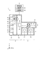
<基板処理システムの構成>
まず、実施形態に係る基板処理システム1(基板処理装置の一例)の構成について図1および図2を参照して説明する。図1は、実施形態に係る基板処理システム1を上方から見た模式的な断面図である。また、図2は、実施形態に係る基板処理システム1を側方から見た模式的な断面図である。なお、以下では、位置関係を明確にするために、互いに直交するX軸、Y軸およびZ軸を規定し、Z軸正方向を鉛直上向き方向とする。
<Structure of substrate processing system>
First, a configuration of a substrate processing system 1 (an example of a substrate processing apparatus) according to the embodiment will be described with reference to FIGS. FIG. 1 is a schematic cross-sectional view of a
図1に示すように、基板処理システム1は、搬入出ステーション2と、処理ステーション3とを備える。搬入出ステーション2と処理ステーション3とは隣接して設けられる。
As shown in FIG. 1, the
搬入出ステーション2は、キャリア載置部11と、搬送部12とを備える。キャリア載置部11には、複数枚の半導体ウェハW(以下、「ウェハW」と記載する)を水平状態で収容する複数のキャリアCが載置される。
The loading /
搬送部12は、キャリア載置部11に隣接して設けられる。搬送部12の内部には、搬送装置13と受渡部14とが配置される。
The
搬送装置13は、ウェハWを保持するウェハ保持機構を備える。また、搬送装置13は、水平方向および鉛直方向への移動ならびに鉛直軸を中心とする旋回が可能であり、ウェハ保持機構を用いてキャリアCと受渡部14との間でウェハWの搬送を行う。
The
処理ステーション3は、搬送部12に隣接して設けられる。処理ステーション3は、搬送ブロック4と、複数の処理ブロック5とを備える。
The
搬送ブロック4は、搬送エリア15と、搬送装置16とを備える。搬送エリア15は、たとえば、搬入出ステーション2および処理ステーション3の並び方向(X軸方向)に沿って延在する直方体状の領域である。搬送エリア15には、搬送装置16が配置される。
The transport block 4 includes a
搬送装置16は、ウェハWを保持するウェハ保持機構を備える。また、搬送装置16は、水平方向および鉛直方向への移動ならびに鉛直軸を中心とする旋回が可能であり、ウェハ保持機構を用いて受渡部14と複数の処理ブロック5との間でウェハWの搬送を行う。
The
複数の処理ブロック5は、搬送エリア15の一方側において搬送エリア15に隣接して配置される。具体的には、複数の処理ブロック5は、搬入出ステーション2および処理ステーション3の並び方向(X軸方向)に直交する方向(Y軸方向)における搬送エリア15の一方側(図ではY軸負方向側)に配置される。
The plurality of
また、図2に示すように、複数の処理ブロック5は、鉛直方向に沿って多段に配置される。実施形態において、複数の処理ブロック5の段数は3段であるが、複数の処理ブロック5の段数は3段に限定されない。
Further, as shown in FIG. 2, the plurality of
このように、実施形態に係る基板処理システム1において、複数の処理ブロック5は、搬送ブロック4の一方側において多段に配置される。そして、各段に配置された処理ブロック5と受渡部14との間で行われるウェハWの搬送は、搬送ブロック4に配置された共通の搬送装置16によって行われる。
As described above, in the
各処理ブロック5は、液処理ユニット17と、乾燥ユニット18とを備える。液処理ユニット17は第1処理部の一例であり、乾燥ユニット18は第2処理部の一例である。
Each
液処理ユニット17は、ウェハWのパターン形成面である上面を洗浄する洗浄処理を行う。かかる洗浄処理は、第1処理の一例である。なお、以下に説明する実施形態では、第1処理として洗浄処理を行う例について示すが、かかる第1処理は洗浄処理に限られない。
The
さらに、液処理ユニット17は、洗浄処理後のウェハWの上面に液膜を形成する液膜形成処理を行う。液処理ユニット17の構成については後述する。
Further, the
乾燥ユニット18は、液膜形成処理後のウェハWに対して超臨界乾燥処理を行う。具体的には、乾燥ユニット18は、液膜形成処理後のウェハWを超臨界状態の処理流体(以下、「超臨界流体」とも呼称する。)と接触させることによって同ウェハWを乾燥させる。かかる超臨界乾燥処理は、第2処理の一例である。
The drying
なお、以下に説明する実施形態では、第2処理として超臨界乾燥処理を行う例について示すが、かかる第2処理は超臨界乾燥処理に限られず、スピン乾燥処理などその他の乾燥処理であってもよい。さらに、第2処理は乾燥処理に限られず、液処理などであってもよい。乾燥ユニット18の構成については後述する。
In the embodiment described below, an example in which a supercritical drying process is performed as the second process is described. However, the second process is not limited to the supercritical drying process, and may be another drying process such as a spin drying process. Good. Further, the second processing is not limited to the drying processing, and may be a liquid processing or the like. The configuration of the drying
なお、図1および図2には図示していないが、基板処理システム1は、乾燥ユニット18に対して処理流体を供給する供給ユニットを有する。具体的には、かかる供給ユニットは、流量計、流量調整器、背圧弁、ヒータなどを含む供給機器群と、供給機器群を収容する筐体とを備える。実施形態において、供給ユニットは、処理流体としてCO2を乾燥ユニット18に供給する。
Although not shown in FIGS. 1 and 2, the
液処理ユニット17および乾燥ユニット18は、搬送エリア15に沿って(すなわち、X軸方向に沿って)並べられる。液処理ユニット17および乾燥ユニット18のうち、液処理ユニット17は、搬入出ステーション2に近い位置に配置され、乾燥ユニット18は、搬入出ステーション2から遠い位置に配置される。
The
このように、各処理ブロック5は、液処理ユニット17および乾燥ユニット18をそれぞれ1つずつ備える。すなわち、基板処理システム1には、液処理ユニット17および乾燥ユニット18が同じ数だけ設けられる。
As described above, each
図1に示すように、基板処理システム1は、制御装置6を備える。制御装置6は、たとえばコンピュータであり、制御部61と記憶部62とを備える。
As shown in FIG. 1, the
制御部61は、CPU(Central Processing Unit)、ROM(Read Only Memory)、RAM(Random Access Memory)、入出力ポートなどを有するマイクロコンピュータや各種の回路を含む。かかるマイクロコンピュータのCPUは、ROMに記憶されているプログラムを読み出して実行することにより、搬送装置13、16、液処理ユニット17および乾燥ユニット18等の制御を実現する。
The
なお、かかるプログラムは、コンピュータによって読み取り可能な記憶媒体に記憶されていたものであって、その記憶媒体から制御装置6の記憶部62にインストールされたものであってもよい。コンピュータによって読み取り可能な記憶媒体としては、たとえばハードディスク(HD)、フレキシブルディスク(FD)、コンパクトディスク(CD)、マグネットオプティカルディスク(MO)、メモリカードなどがある。
The program may be stored in a storage medium readable by a computer, and may be installed in the
記憶部62は、たとえば、RAM、フラッシュメモリ(Flash Memory)などの半導体メモリ素子、または、ハードディスク、光ディスクなどの記憶装置によって実現される。
The
<液処理ユニットの構成>
次に、液処理ユニット17の構成について、図3を参照しながら説明する。図3は、液処理ユニット17の構成例を示す図である。液処理ユニット17は、たとえば、スピン洗浄によりウェハWを1枚ずつ洗浄する枚葉式の洗浄装置として構成される。
<Structure of liquid processing unit>
Next, the configuration of the
図3に示すように、液処理ユニット17は、処理空間を形成するアウターチャンバー23内に配置されたウェハ保持機構25にてウェハWをほぼ水平に保持し、このウェハ保持機構25を鉛直軸周りに回転させることによりウェハWを回転させる。
As shown in FIG. 3, the
そして、液処理ユニット17は、回転するウェハWの上方にノズルアーム26を進入させ、かかるノズルアーム26の先端部に設けられる薬液ノズル26aから薬液やリンス液を予め定められた順に供給することにより、ウェハW上面の洗浄処理を行う。
Then, the
また、液処理ユニット17には、ウェハ保持機構25の内部にも薬液供給路25aが形成されている。そして、かかる薬液供給路25aから供給された薬液やリンス液によって、ウェハWの下面も洗浄される。
In the
洗浄処理は、たとえば、最初にアルカリ性の薬液であるSC1液(アンモニアと過酸化水素水の混合液)によるパーティクルや有機性の汚染物質の除去が行われる。次に、リンス液である脱イオン水(DeIonized Water:以下、「DIW」と記載する)によるリンス洗浄が行われる。 In the cleaning process, for example, first, particles or organic contaminants are removed by an SC1 solution (a mixed solution of ammonia and hydrogen peroxide) which is an alkaline chemical solution. Next, rinsing with de-ionized water (hereinafter, referred to as “DIW”) as a rinsing liquid is performed.
次に、酸性薬液である希フッ酸水溶液(Diluted HydroFluoric acid:以下、「DHF」と記載する)による自然酸化膜の除去が行われ、次に、DIWによるリンス洗浄が行われる。 Next, a natural oxide film is removed by a dilute hydrofluoric acid aqueous solution (Diluted HydroFluoric acid: hereinafter, referred to as “DHF”), which is an acidic chemical, and then rinsed with DIW.
上述の各種薬液は、アウターチャンバー23や、アウターチャンバー23内に配置されるインナーカップ24に受け止められて、アウターチャンバー23の底部に設けられる排液口23aや、インナーカップ24の底部に設けられる排液口24aから排出される。さらに、アウターチャンバー23内の雰囲気は、アウターチャンバー23の底部に設けられる排気口23bから排気される。
The above-mentioned various chemicals are received by the
液膜形成処理は、洗浄処理におけるリンス処理の後に行われる。具体的には、液処理ユニット17は、ウェハ保持機構25を回転させながら、ウェハWの上面および下面に液体状態のIPA(以下、「IPA液体」とも呼称する)を供給する。これにより、ウェハWの両面に残存するDIWがIPAに置換される。その後、液処理ユニット17は、ウェハ保持機構25の回転を緩やかに停止する。
The liquid film forming process is performed after the rinsing process in the cleaning process. Specifically, the
液膜形成処理を終えたウェハWは、その上面にIPA液体の液膜が形成された状態のまま、ウェハ保持機構25に設けられた不図示の受け渡し機構により搬送装置16に受け渡され、液処理ユニット17から搬出される。
The wafer W that has completed the liquid film forming process is transferred to the
ウェハW上に形成された液膜は、液処理ユニット17から乾燥ユニット18へのウェハWの搬送中や、乾燥ユニット18への搬入動作中に、ウェハW上面の液体が蒸発(気化)することによってパターン倒れが発生することを防止する。
The liquid film formed on the wafer W evaporates (vaporizes) on the upper surface of the wafer W during the transfer of the wafer W from the
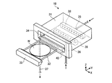
<乾燥ユニットの概要>
つづいて、乾燥ユニット18の構成について、図4を参照しながら説明する。図4は、乾燥ユニット18の構成例を示す模式斜視図である。
<Outline of drying unit>
Next, the configuration of the drying
乾燥ユニット18は、本体31と、保持板32と、蓋部材33とを有する。筐体状の本体31には、ウェハWを搬入出するための開口部34が形成される。保持板32は、処理対象のウェハWを水平方向に保持する。蓋部材33は、かかる保持板32を支持するとともに、ウェハWを本体31内に搬入したときに、開口部34を密閉する。
The drying
本体31は、たとえば直径300mmのウェハWを収容可能な処理空間が内部に形成された容器であり、その壁部には、供給ポート35、36と排出ポート37とが設けられる。供給ポート35、36および排出ポート37は、それぞれ、乾燥ユニット18に超臨界流体を流通させるための供給流路および排出流路に接続されている。
The
供給ポート35は、筐体状の本体31において、開口部34とは反対側の側面に接続されている。また、供給ポート36は、本体31の底面に接続されている。さらに、排出ポート37は、開口部34の下方側に接続されている。なお、図4には2つの供給ポート35、36と1つの排出ポート37が図示されているが、供給ポート35、36や排出ポート37の数は特に限定されない。
The
また、本体31の内部には、流体供給ヘッダー38、39と、流体排出ヘッダー40とが設けられる。そして、流体供給ヘッダー38、39には複数の供給口がかかる流体供給ヘッダー38,39の長手方向に並んで形成され、流体排出ヘッダー40には複数の排出口がかかる流体排出ヘッダー40の長手方向に並んで形成される。
Further, inside the
流体供給ヘッダー38は、供給ポート35に接続され、筐体状の本体31内部において、開口部34とは反対側の側面に隣接して設けられる。また、流体供給ヘッダー38に並んで形成される複数の供給口は、開口部34側を向いている。
The fluid supply header 38 is connected to the
流体供給ヘッダー39は、供給ポート36に接続され、筐体状の本体31内部における底面の中央部に設けられる。また、流体供給ヘッダー39に並んで形成される複数の供給口は、上方を向いている。
The
流体排出ヘッダー40は、排出ポート37に接続され、筐体状の本体31内部において、開口部34側の側面に隣接するとともに、開口部34より下方に設けられる。また、流体排出ヘッダー40に並んで形成される複数の排出口は、上方を向いている。
The
流体供給ヘッダー38、39は、超臨界流体を本体31内に供給する。また、流体排出ヘッダー40は、本体31内の超臨界流体を本体31の外部に導いて排出する。なお、流体排出ヘッダー40を介して本体31の外部に排出される超臨界流体には、ウェハWの表面から超臨界状態の超臨界流体に溶け込んだIPA液体が含まれる。
かかる乾燥ユニット18内において、ウェハW上に形成されているパターンの間のIPA液体は、高圧状態(たとえば、16MPa)である超臨界流体と接触することで、徐々に超臨界流体に溶解し、パターンの間は徐々に超臨界流体と置き換わる。そして、最終的には、超臨界流体のみによってパターンの間が満たされる。
In the drying
そして、パターンの間からIPA液体が除去された後に、本体31内部の圧力を高圧状態から大気圧まで減圧することによって、CO2は超臨界状態から気体状態に変化し、パターンの間は気体のみによって占められる。このようにしてパターンの間のIPA液体は除去され、ウェハWの乾燥処理が完了する。
Then, after the IPA liquid is removed from between the patterns, the pressure inside the
ここで、超臨界流体は、液体(たとえばIPA液体)と比べて粘度が小さく、また液体を溶解する能力も高いことに加え、超臨界流体と平衡状態にある液体や気体との間で界面が存在しない。これにより、超臨界流体を用いた乾燥処理では、表面張力の影響を受けることなく液体を乾燥させることができる。したがって、実施形態によれば、乾燥処理の際にパターンが倒れることを抑制することができる。 Here, the supercritical fluid has a lower viscosity than a liquid (for example, an IPA liquid), has a higher ability to dissolve the liquid, and has an interface between the supercritical fluid and the liquid or gas in an equilibrium state. not exist. Thereby, in the drying treatment using the supercritical fluid, the liquid can be dried without being affected by the surface tension. Therefore, according to the embodiment, it is possible to prevent the pattern from falling down during the drying process.
なお、実施形態では、乾燥防止用の液体としてIPA液体を用い、処理流体として超臨界状態のCO2を用いた例について示しているが、IPA以外の液体を乾燥防止用の液体として用いてもよいし、超臨界状態のCO2以外の流体を処理流体として用いてもよい。 In the embodiment, an example is described in which an IPA liquid is used as a liquid for preventing drying, and CO 2 in a supercritical state is used as a processing fluid. However, a liquid other than IPA may be used as a liquid for preventing drying. Alternatively, a fluid other than CO 2 in a supercritical state may be used as the processing fluid.
<基板処理フロー>
次に、上述した基板処理システム1におけるウェハWの処理フローについて、図5を参照しながら説明する。図5は、実施形態に係る基板処理システム1において実行される一連の基板処理の手順を示すフローチャートである。なお、図5に示す一連の基板処理は、制御部61の制御に従って実行される。
<Substrate processing flow>
Next, a processing flow of the wafer W in the above-described
基板処理システム1では、まず、搬送装置13がキャリアCからウェハWを取り出して受渡部14へ載置する(ステップS101)。つづいて、基板処理システム1では、搬送装置16がウェハWを受渡部14から取り出して液処理ユニット17に搬送する第1搬送処理が行われる(ステップS102)。なお、以降の図面では、かかる第1搬送処理を「T1」とも記載する。
In the
つづいて、基板処理システム1では、液処理ユニット17において第1処理(実施形態では洗浄処理)が行われる(ステップS103)。液処理ユニット17は、たとえば、ウェハWのパターン形成面である上面に各種の処理液を供給することにより、ウェハWの上面からパーティクルや自然酸化膜等を除去する。
Subsequently, in the
つづいて、基板処理システム1では、液処理ユニット17において液膜形成処理が行われる(ステップS104)。液処理ユニット17は、たとえば、洗浄処理後のウェハWの上面にIPA液体を供給することにより、ウェハWの上面にIPA液体による液膜を形成する。なお、以降の図面では、液処理ユニット17で実施される第1処理および液膜形成処理を総称して「SPIN」とも記載する。
Subsequently, in the
つづいて、基板処理システム1では、搬送装置16が液膜が形成されたウェハWを液処理ユニット17から取り出して乾燥ユニット18に搬送する第2搬送処理が行われる(ステップS105)。なお、以降の図面では、かかる第2搬送処理を「T2」とも記載する。
Subsequently, in the
そして、基板処理システム1では、乾燥ユニット18において第2処理(実施形態では超臨界乾燥処理)が行われる(ステップS106)。かかる超臨界乾燥処理において、乾燥ユニット18は、液膜形成処理後のウェハWを超臨界流体と接触させることによって液膜形成処理後のウェハWを乾燥させる。なお、以降の図面では、かかる第2処理を「SCC」とも記載する。
Then, in the
つづいて、基板処理システム1では、搬送装置16が超臨界乾燥処理されたウェハWを乾燥ユニット18から取り出して受渡部14に搬送する第3搬送処理が行われる(ステップS107)。なお、以降の図面では、かかる第3搬送処理を「T3」とも記載する。
Subsequently, in the
最後に、基板処理システム1では、搬送装置13が受渡部14からウェハWを取り出してキャリアCへ搬出する(ステップS108)。かかる搬出処理を終えると、1枚のウェハWについての一連の基板処理が終了する。
Finally, in the
ここで、この一連の基板処理において、液膜形成処理されたウェハWが第2搬送処理されるタイミングで他のウェハWが搬送装置16で搬送処理されていると、液膜が形成されたウェハWは、他のウェハWの搬送処理が完了するまでそのまま待機しなければならない。
Here, in this series of substrate processing, if another wafer W is transferred by the
そして、待機している間に液膜が乾燥するなどして、ウェハW表面の液膜状態が変化した場合、その後の超臨界乾燥処理においてウェハW上に形成されているパターンが倒れるなどの不具合が発生することから、ウェハWの歩留まりが低下してしまう恐れがあった。 If the state of the liquid film on the surface of the wafer W changes due to drying of the liquid film while waiting, the pattern formed on the wafer W in the subsequent supercritical drying process may fall. , The yield of the wafer W may be reduced.
そこで、実施形態では、ウェハWが第1搬送処理される前に、第1搬送処理の開始タイミングを所定の手順で設定する開始タイミング設定処理を行う。かかる処理により、液膜形成処理されたウェハWが第2搬送処理されるタイミングで他のウェハWが搬送装置16で搬送処理されることを抑制することができる。
Therefore, in the embodiment, before the wafer W is subjected to the first transfer processing, a start timing setting processing for setting a start timing of the first transfer processing in a predetermined procedure is performed. By such processing, it is possible to suppress the transfer processing of another wafer W by the
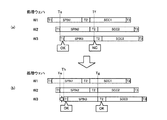
<開始タイミング設定処理の詳細>
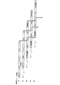
つづいて、第1搬送処理の開始タイミング設定処理の詳細について、図6〜図11を参照しながら説明する。図6〜図11は、実施形態に係る第1搬送処理の開始タイミング設定処理を説明するためのタイミングチャート(1)〜(6)である。なお、図6〜図11に示す第1搬送処理の開始タイミング設定処理は、制御部61の制御に従って実行される。
<Details of start timing setting process>
Next, details of the start timing setting process of the first transport process will be described with reference to FIGS. 6 to 11 are timing charts (1) to (6) for explaining a start timing setting process of the first transport process according to the embodiment. The start timing setting process of the first transport process shown in FIGS. 6 to 11 is executed under the control of the
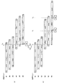
また、以下に示す実施形態では、3組の液処理ユニット17および乾燥ユニット18がそれぞれペアになって連続的に基板処理を行う場合について示す。そして、1組目の液処理ユニット17で行われる第1処理および液膜形成処理を「SPIN1」と記載し、1組目の乾燥ユニット18で行われる超臨界乾燥処理を「SCC1」と記載する。
In the embodiment described below, a case is described in which three sets of the
同様に、2組目の液処理ユニット17で行われる第1処理および液膜形成処理を「SPIN2」と記載し、2組目の乾燥ユニット18で行われる超臨界乾燥処理を「SCC2」と記載する。さらに、3組目の液処理ユニット17で行われる第1処理および液膜形成処理を「SPIN3」と記載し、3組目の乾燥ユニット18で行われる超臨界乾燥処理を「SCC3」と記載する。
Similarly, the first process and the liquid film forming process performed in the second set of
図6の(a)に示すように、基板処理システム1で1枚目のウェハW1が第1搬送処理(T1)を開始した後、2枚目のウェハW2で第1搬送処理が開始される前に、かかるウェハW2に対する第1搬送処理の開始タイミング設定処理が行われる。
As shown in FIG. 6A, after the first wafer W1 starts the first transfer process (T1) in the
最初に、制御部61は、直前に投入されたウェハW1で第1搬送処理が終了するタイミングTaを、ウェハW2における第1搬送処理の開始タイミングに設定する。次に、制御部61は、ウェハW2が第1処理される予定の2組目の液処理ユニット17(すなわちSPIN2)で他のウェハWが処理中でないか否かを判定する。
First, the
ここで、図6の(a)に示した状態では、ウェハW2が第1処理される予定の2組目の液処理ユニット17は他のウェハWを処理中ではない。そこで、制御部61は、ウェハW2が第1搬送処理されるタイミングと他のウェハWが搬送処理されるタイミングとが重複しないか否かを判定する。
Here, in the state shown in FIG. 6A, the second set of
ここで、図6の(a)に示した状態では、ウェハW2の第1搬送処理が他のウェハWの搬送処理と重複していない。そこで、制御部61は、ウェハW2が第2搬送処理(T2)されるタイミングと他のウェハWが搬送処理されるタイミングとが重複しないか否かを判定する。
Here, in the state shown in FIG. 6A, the first transfer processing of the wafer W2 does not overlap with the transfer processing of another wafer W. Therefore, the
ここで、図6の(a)に示した状態では、ウェハW2における第2搬送処理の開始タイミングTbでウェハW1が第2搬送処理されている。そこで、制御部61は、図6の(b)に示すように、ウェハW2における第2搬送処理の開始タイミングを、ウェハW1における第2搬送処理の終了タイミングTcにシフトさせる。
Here, in the state shown in FIG. 6A, the second transfer processing of the wafer W1 is performed at the start timing Tb of the second transfer processing of the wafer W2. Therefore, the
なぜなら、ウェハW1における第2搬送処理の終了タイミングTcは、他のウェハWの搬送処理と重複しない最前のタイミングだからである。このように、他のウェハWの搬送処理と重複しない最前のタイミングにシフトさせることにより、余分な待機時間が少なくなることから、基板処理システム1におけるウェハWのスループットを向上させることができる。
This is because the end timing Tc of the second transfer processing on the wafer W1 is the earliest timing that does not overlap with the transfer processing of another wafer W. As described above, by shifting to the earliest timing that does not overlap with the transfer processing of another wafer W, an extra standby time is reduced, and thus the throughput of the wafer W in the
そして、かかる第2搬送処理のシフトに伴い、制御部61は、ウェハW2における第1搬送処理の開始タイミングをTaからTdにシフトさせる。
Then, with the shift of the second transfer processing, the
つぎに、制御部61は、ウェハW2が第1搬送処理される新たなタイミングと他のウェハWが搬送処理されるタイミングとが重複しないか否かを判定する。ここで、図6の(b)に示した状態において、ウェハW2における第1搬送処理のタイミングでは他のウェハWが搬送処理されていない。
Next, the
すなわち、図6の(b)に示した状態では、ウェハW2の第1搬送処理および第2搬送処理がいずれも他のウェハWの搬送処理と重複していない。したがって、制御部61は、新たに設定された開始タイミングTdをウェハW2の第1搬送処理の開始タイミングとして設定する。そして、制御部61は、設定された開始タイミングTdでウェハW2の第1搬送処理を開始する。
That is, in the state shown in FIG. 6B, neither the first transfer processing of the wafer W2 nor the second transfer processing overlaps with the transfer processing of another wafer W. Therefore, the
つづいて、図7の(a)に示すように、3枚目のウェハW3で第1搬送処理が開始される前に、かかるウェハW3に対する第1搬送処理の開始タイミング設定処理が行われる。 Subsequently, as shown in FIG. 7A, before the first transfer processing is started on the third wafer W3, the start timing setting processing of the first transfer processing for the wafer W3 is performed.
最初に、制御部61は、直前に投入されたウェハW2で第1搬送処理が終了するタイミングTeを、ウェハW3における第1搬送処理の開始タイミングに設定する。次に、制御部61は、ウェハW3が第1処理される予定の3組目の液処理ユニット17(すなわちSPIN3)で他のウェハWが処理中でないか否かを判定する。
First, the
ここで、図7の(a)に示した状態では、ウェハW3が第1処理される予定の3組目の液処理ユニット17は他のウェハWを処理中ではない。そこで、制御部61は、ウェハW3が第1搬送処理されるタイミングと他のウェハWが搬送処理されるタイミングとが重複しないか否かを判定する。
Here, in the state shown in FIG. 7A, the third set of
ここで、図7の(a)に示した状態では、ウェハW3の第1搬送処理が他のウェハWの搬送処理と重複していない。そこで、制御部61は、ウェハW3が第2搬送処理されるタイミングと他のウェハWが搬送処理されるタイミングとが重複しないか否かを判定する。
Here, in the state shown in FIG. 7A, the first transfer processing of the wafer W3 does not overlap with the transfer processing of another wafer W. Therefore, the
ここで、図7の(a)に示した状態では、ウェハW3における第2搬送処理の開始タイミングTfでウェハW2が第2搬送処理されている。そこで、制御部61は、図7の(b)に示すように、ウェハW3における第2搬送処理の開始タイミングを、ウェハW2における第2搬送処理の終了タイミングTgにシフトさせる。
Here, in the state shown in FIG. 7A, the second transfer processing of the wafer W2 is performed at the start timing Tf of the second transfer processing of the wafer W3. Therefore, as shown in FIG. 7B, the
そして、かかる第2搬送処理のシフトに伴い、制御部61は、ウェハW3における第1搬送処理の開始タイミングをTeからThにシフトさせる。
Then, with the shift of the second transfer process, the
つぎに、制御部61は、ウェハW3が第1搬送処理される新たなタイミングと他のウェハWが搬送処理されるタイミングとが重複しないか否かを判定する。ここで、図7の(b)に示した状態において、ウェハW3における第1搬送処理のタイミングでは他のウェハWが搬送処理されていない。
Next, the
すなわち、図7の(b)に示した状態では、ウェハW3の第1搬送処理および第2搬送処理がいずれも他のウェハWの搬送処理と重複していない。したがって、制御部61は、新たに設定された開始タイミングThをウェハW3の第1搬送処理の開始タイミングとして設定する。そして、制御部61は、設定された開始タイミングThでウェハW3の第1搬送処理を開始する。
That is, in the state shown in FIG. 7B, neither the first transfer processing nor the second transfer processing of the wafer W3 overlaps with the transfer processing of another wafer W. Therefore, the
つづいて、図8の(a)に示すように、4枚目のウェハW4で第1搬送処理が開始される前に、かかるウェハW4に対する第1搬送処理の開始タイミング設定処理が行われる。 Subsequently, as shown in FIG. 8A, before the first transfer process is started on the fourth wafer W4, the start timing setting process of the first transfer process is performed on the wafer W4.
最初に、制御部61は、直前に投入されたウェハW3で第1搬送処理が終了するタイミングTiを、ウェハW4における第1搬送処理の開始タイミングに設定する。次に、制御部61は、ウェハW4が第1処理される予定の1組目の液処理ユニット17(すなわちSPIN1)で他のウェハWが処理中でないか否かを判定する。
First, the
ここで、図8の(a)に示した状態では、ウェハW4が第1処理される予定の1組目の液処理ユニット17は他のウェハW1を処理中である。そこで、制御部61は、図8の(b)に示すように、ウェハW4における第1搬送処理の開始タイミングを、ウェハW3における第2搬送処理の終了タイミングTjにシフトさせる。
Here, in the state shown in FIG. 8A, the first set of
なぜなら、ウェハW3における第2搬送処理の終了タイミングTjは、1組目の液処理ユニット17での処理および他のウェハWの搬送処理と重複しない最前のタイミングだからである。
This is because the end timing Tj of the second transfer processing on the wafer W3 is the earliest timing that does not overlap the processing in the first set of
このように、使用する液処理ユニット17での処理および他のウェハWの搬送処理と重複しない最前のタイミングにシフトさせることにより、余分な待機時間が少なくなることから、基板処理システム1におけるウェハWのスループットを向上させることができる。
As described above, by shifting the processing to the first timing that does not overlap with the processing in the
次に、制御部61は、ウェハW4が第2搬送処理されるタイミングと他のウェハWが搬送処理されるタイミングとが重複しないか否かを判定する。
Next, the
ここで、図8の(b)に示した状態では、ウェハW4における第2搬送処理のタイミングのうち、タイミングTkでウェハW3が第3搬送処理される。そこで、制御部61は、図8の(c)に示すように、ウェハW4における第2搬送処理の開始タイミングを、ウェハW3における第3搬送処理の終了タイミングTlにシフトさせる。
Here, in the state shown in FIG. 8B, the third transfer processing of the wafer W3 is performed at the timing Tk among the timings of the second transfer processing of the wafer W4. Therefore, the
そして、かかる第2搬送処理のシフトに伴い、制御部61は、ウェハW4における第1搬送処理の開始タイミングをTjからTmにシフトさせる。
Then, with the shift of the second transfer processing, the
つぎに、制御部61は、ウェハW4が第1搬送処理される新たなタイミングと他のウェハWが搬送処理されるタイミングとが重複しないか否かを判定する。ここで、図8の(c)に示した状態において、ウェハW4における第1搬送処理のタイミングでは他のウェハWが搬送処理されていない。
Next, the
すなわち、図8の(c)に示した状態では、ウェハW4の第1搬送処理および第2搬送処理がいずれも他のウェハWの搬送処理と重複していない。したがって、制御部61は、新たに設定された開始タイミングTmをウェハW4の第1搬送処理の開始タイミングとして設定する。そして、制御部61は、設定された開始タイミングTmでウェハW4の第1搬送処理を開始する。
That is, in the state illustrated in FIG. 8C, neither the first transfer process nor the second transfer process of the wafer W4 overlaps with the transfer process of another wafer W. Therefore, the
つづいて、図9の(a)に示すように、5枚目のウェハW5で第1搬送処理が開始される前に、かかるウェハW5に対する第1搬送処理の開始タイミング設定処理が行われる。 Subsequently, as shown in FIG. 9A, before the first transfer process is started on the fifth wafer W5, a start timing setting process of the first transfer process on the wafer W5 is performed.
最初に、制御部61は、直前に投入されたウェハW4で第1搬送処理が終了するタイミングTnを、ウェハW5における第1搬送処理の開始タイミングに設定する。次に、制御部61は、ウェハW5が第1処理される予定の2組目の液処理ユニット17で他のウェハWが処理中でないか否かを判定する。
First, the
ここで、図9の(a)に示した状態では、ウェハW5が第1処理される予定の2組目の液処理ユニット17は他のウェハWを処理中ではない。そこで、制御部61は、ウェハW5が第1搬送処理されるタイミングと他のウェハWが搬送処理されるタイミングとが重複しないか否かを判定する。
Here, in the state shown in FIG. 9A, the second set of
ここで、図9の(a)に示した状態では、ウェハW5の第1搬送処理が他のウェハWの搬送処理と重複していない。そこで、制御部61は、ウェハW5が第2搬送処理されるタイミングと他のウェハWが搬送処理されるタイミングとが重複しないか否かを判定する。
Here, in the state shown in FIG. 9A, the first transfer processing of the wafer W5 does not overlap with the transfer processing of another wafer W. Therefore, the
ここで、図9の(a)に示した状態では、ウェハW5における第2搬送処理の開始タイミングToでウェハW4が第2搬送処理されている。そこで、制御部61は、図9の(b)に示すように、ウェハW5における第2搬送処理の開始タイミングを、ウェハW4における第2搬送処理の終了タイミングTpにシフトさせる。
Here, in the state shown in FIG. 9A, the second transfer processing of the wafer W4 is performed at the start timing To of the second transfer processing of the wafer W5. Therefore, as shown in FIG. 9B, the
そして、かかる第2搬送処理のシフトに伴い、制御部61は、ウェハW5における第1搬送処理の開始タイミングをTnからTqにシフトさせる。
Then, with the shift of the second transfer process, the
つぎに、制御部61は、ウェハW5が第1搬送処理される新たなタイミングと他のウェハWが搬送処理されるタイミングとが重複しないか否かを判定する。ここで、図9の(b)に示した状態において、ウェハW5における第1搬送処理のタイミングでは他のウェハWが搬送処理されていない。
Next, the
すなわち、図9の(b)に示した状態では、ウェハW5の第1搬送処理および第2搬送処理がいずれも他のウェハWの搬送処理と重複していない。したがって、制御部61は、新たに設定された開始タイミングTqをウェハW5の第1搬送処理の開始タイミングとして設定する。そして、制御部61は、設定された開始タイミングTqでウェハW5の第1搬送処理を開始する。
That is, in the state shown in FIG. 9B, neither the first transfer processing nor the second transfer processing of the wafer W5 overlaps with the transfer processing of another wafer W. Therefore, the
つづいて、図10の(a)に示すように、6枚目のウェハW6で第1搬送処理が開始される前に、かかるウェハW6に対する第1搬送処理の開始タイミング設定処理が行われる。 Subsequently, as shown in FIG. 10A, before the first transfer process is started on the sixth wafer W6, a start timing setting process of the first transfer process for the wafer W6 is performed.
最初に、制御部61は、直前に投入されたウェハW5で第1搬送処理が終了するタイミングTrを、ウェハW6における第1搬送処理の開始タイミングに設定する。次に、制御部61は、ウェハW6が第1処理される予定の3組目の液処理ユニット17で他のウェハWが処理中でないか否かを判定する。
First, the
ここで、図10の(a)に示した状態では、ウェハW6が第1処理される予定の3組目の液処理ユニット17は他のウェハWを処理中ではない。そこで、制御部61は、ウェハW6が第1搬送処理されるタイミングと他のウェハWが搬送処理されるタイミングとが重複しないか否かを判定する。
Here, in the state shown in FIG. 10A, the third set of
ここで、図10の(a)に示した状態では、ウェハW6における第1搬送処理のタイミングのうち、タイミングTsでウェハW1が第3搬送処理される。そこで、制御部61は、図10の(b)に示すように、ウェハW6における第1搬送処理の開始タイミングを、ウェハW5における第2搬送処理の終了タイミングTtにシフトさせる。
Here, in the state shown in FIG. 10A, the third transfer processing of the wafer W1 is performed at the timing Ts among the timings of the first transfer processing of the wafer W6. Thus, as shown in FIG. 10B, the
なぜなら、ウェハW5における第2搬送処理の終了タイミングTtは、他のウェハWの搬送処理と重複しない最前のタイミングだからである。 This is because the end timing Tt of the second transfer processing on the wafer W5 is the earliest timing that does not overlap with the transfer processing of another wafer W.
次に、制御部61は、ウェハW6が第2搬送処理されるタイミングと他のウェハWが搬送処理されるタイミングとが重複しないか否かを判定する。
Next, the
ここで、図10の(b)に示した状態では、ウェハW6における第2搬送処理のタイミングのうち、タイミングTuでウェハW3が第3搬送処理される。そこで、制御部61は、図11に示すように、ウェハW6における第2搬送処理の開始タイミングを、ウェハW5における第3搬送処理の終了タイミングTvにシフトさせる。
Here, in the state shown in FIG. 10B, of the timing of the second transfer processing on the wafer W6, the third transfer processing of the wafer W3 is performed at the timing Tu. Therefore, as shown in FIG. 11, the
そして、かかる第2搬送処理のシフトに伴い、制御部61は、ウェハW6における第1搬送処理の開始タイミングをTtからTwにシフトさせる。
Then, with the shift of the second transfer process, the
つぎに、制御部61は、ウェハW6が第1搬送処理される新たなタイミングと他のウェハWが搬送処理されるタイミングとが重複しないか否かを判定する。ここで、図11に示した状態において、ウェハW6における第1搬送処理のタイミングでは他のウェハWが搬送処理されていない。
Next, the
すなわち、図11に示した状態では、ウェハW6の第1搬送処理および第2搬送処理がいずれも他のウェハWの搬送処理と重複していない。したがって、制御部61は、新たに設定された開始タイミングTwをウェハW6の第1搬送処理の開始タイミングとして設定する。そして、制御部61は、設定された開始タイミングTwでウェハW6の第1搬送処理を開始する。
That is, in the state shown in FIG. 11, neither the first transfer process nor the second transfer process of the wafer W6 overlaps with the transfer process of another wafer W. Therefore, the
ここまで説明した処理を行うことにより、複数ペアの液処理ユニット17および乾燥ユニット18と受渡部14との間を共通の搬送装置16で複数のウェハWの搬送を行う場合に、各ウェハWの搬送処理と重複することを抑制することができる。
By performing the processing described so far, when a plurality of pairs of the
すなわち、液膜形成処理されたウェハWが第2搬送処理されるタイミングで他のウェハWが搬送装置16で搬送処理されることを抑制することができる。したがって、実施形態によれば、表面に液膜が形成されたウェハWを搬送する際に、搬送時間がばらつくことを抑制することができる。
That is, it is possible to prevent another wafer W from being transported by the
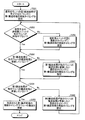
<開始タイミング設定処理の手順>
つづいて、実施形態に係る第1搬送処理の開始タイミング設定処理の手順について、図12を参照しながら説明する。図12は、実施形態に係る第1搬送処理の開始タイミング設定処理の手順を示すフローチャートである。
<Start timing setting procedure>
Subsequently, a procedure of a start timing setting process of the first transport process according to the embodiment will be described with reference to FIG. FIG. 12 is a flowchart illustrating a procedure of a start timing setting process of the first transport process according to the embodiment.
最初に、制御部61は、直前のウェハWの第1搬送処理が終了するタイミングに、対象となるウェハWの第1搬送処理の開始タイミングを設定する(ステップS201)。次に、対象となるウェハWが使用予定の液処理ユニット17で他のウェハWが使用中でないか否かを判定する(ステップS202)。
First, the
そして、使用予定の液処理ユニット17で他のウェハWが使用中でない場合(ステップS202,Yes)、制御部61は、対象となるウェハWの第1搬送処理が他のウェハWの搬送処理と重複していないか否かを判定する(ステップS203)。
When another wafer W is not being used in the
そして、対象となるウェハWの第1搬送処理が他のウェハWの搬送処理と重複していない場合(ステップS203,Yes)、制御部61は、対象となるウェハWの第2搬送処理が他のウェハWの搬送処理と重複していないか否かを判定する(ステップS204)。
If the first transfer processing of the target wafer W does not overlap with the transfer processing of another wafer W (step S203, Yes), the
そして、対象となるウェハWの第2搬送処理が他のウェハWの搬送処理と重複していない場合(ステップS204,Yes)、制御部61は、設定された第1搬送処理の開始タイミングで対象となるウェハWの第1搬送処理を開始する(ステップS205)。そして、対象となるウェハWの開始タイミング設定処理を完了する。
If the second transfer processing of the target wafer W does not overlap with the transfer processing of another wafer W (Step S204, Yes), the
一方、ステップS202で、他のウェハWが使用中である場合(ステップS202,No)、制御部61は、使用予定の液処理ユニット17が空く最前のタイミングに対象となるウェハWの第1搬送処理の開始タイミングを設定する(ステップS206)。そして、ステップS203の処理に移行する。
On the other hand, if another wafer W is being used in step S202 (step S202, No), the
また、ステップS203で、第1搬送処理が他のウェハWの搬送処理と重複する場合(ステップS203,No)、制御部61は、第1搬送処理が他のウェハWの搬送処理と重複しない最前のタイミングに第1搬送処理の開始タイミングを設定する(ステップS207)。そして、ステップS204の処理に移行する。
When the first transfer processing overlaps with the transfer processing of another wafer W in step S203 (No in step S203), the
また、ステップS204で、第2搬送処理が他のウェハWの搬送処理と重複する場合(ステップS204,No)、制御部61は、第2搬送処理が他のウェハWの搬送処理と重複しない最前のタイミングに第1搬送処理の開始タイミングを設定する(ステップS208)。そして、ステップS202の処理に戻る。
When the second transfer processing overlaps with the transfer processing of another wafer W in step S204 (No in step S204), the
実施形態に係る基板処理装置(基板処理システム1)は、複数の第1処理部(液処理ユニット17)と、複数の第2処理部(乾燥ユニット18)と、搬送部(搬送装置16)と、制御部61とを備える。複数の第1処理部は、基板(ウェハW)に第1処理(洗浄処理)を施す。複数の第2処理部は、第1処理が施された基板に第2処理(超臨界乾燥処理)を施す。搬送部は、複数の第1処理部および複数の第2処理部に共通に基板を搬送する。制御部61は、複数の第1処理部、複数の第2処理部および搬送部を制御する。制御部61は、第2搬送処理のタイミングと他の基板が搬送部で搬送されるタイミングとが重複しないように、第1搬送処理の開始タイミングを制御する。なお、第1搬送処理とは基板が第1処理部に搬送される処理のことであり、第2搬送処理とは第1処理された後に液膜が形成された基板が第1処理部から第2処理部に搬送される処理のことである。これにより、表面に液膜が形成されたウェハWを搬送する際に、搬送時間がばらつくことを抑制することができる。
The substrate processing apparatus (substrate processing system 1) according to the embodiment includes a plurality of first processing units (liquid processing units 17), a plurality of second processing units (drying units 18), and a transport unit (transport device 16). , A
また、実施形態に係る基板処理装置において、制御部61は、基板(ウェハW)の第1搬送処理および第2搬送処理のいずれもが、他の基板が搬送部で搬送されるタイミングと重複しない最前のタイミングに、基板の第1搬送処理の開始タイミングを設定する。これにより、基板処理システム1におけるウェハWのスループットを向上させることができる。
Further, in the substrate processing apparatus according to the embodiment, the
また、実施形態に係る基板処理装置において、第1処理は洗浄処理であり、第2処理は液膜が形成された基板(ウェハW)を超臨界流体と接触させて基板を乾燥させる処理(超臨界乾燥処理)である。これにより、乾燥処理の際にウェハWのパターンが倒れることを抑制することができる。 In the substrate processing apparatus according to the embodiment, the first process is a cleaning process, and the second process is a process of contacting a substrate (wafer W) on which a liquid film is formed with a supercritical fluid to dry the substrate (ultra-high-pressure processing). Critical drying treatment). Thereby, it is possible to suppress the pattern of the wafer W from falling down during the drying process.
実施形態に係る基板処理方法は、第1搬送処理と、第2搬送処理と、第3搬送処理と、を含む。第1搬送処理は、第1処理(洗浄処理)を施す複数の第1処理部(液処理ユニット17)のいずれか一つに基板(ウェハW)を搬入する。第2搬送処理は、第2処理(超臨界乾燥処理)を施す複数の第2処理部(乾燥ユニット18)のいずれか一つに第1処理部から基板を搬送する。第3搬送処理は、第2処理部から基板を搬出する。そして、第1処理された後に液膜が形成された基板が第2搬送処理されるタイミングと、他の基板が搬送されるタイミングとが重複しないように、基板の第1搬送処理の開始タイミングを制御する。これにより、表面に液膜が形成されたウェハWを搬送する際に、搬送時間がばらつくことを抑制することができる。 The substrate processing method according to the embodiment includes a first transfer process, a second transfer process, and a third transfer process. In the first transfer processing, the substrate (wafer W) is loaded into any one of the plurality of first processing units (liquid processing units 17) that perform the first processing (cleaning processing). In the second transfer processing, the substrate is transferred from the first processing unit to any one of the plurality of second processing units (drying units 18) that perform the second processing (supercritical drying processing). In the third transfer processing, the substrate is unloaded from the second processing unit. Then, the start timing of the first transfer process of the substrate is set so that the timing at which the substrate on which the liquid film is formed after the first process is subjected to the second transfer process and the timing at which another substrate is transferred do not overlap. Control. Thereby, when transferring the wafer W having the liquid film formed on the surface, it is possible to suppress variations in the transfer time.
<変形例>
つづいては、実施形態の各種変形例について、図13〜図16を参照しながら説明する。図13は、実施形態の変形例1に係る第1搬送処理の開始タイミング設定処理の手順を説明するためのタイミングチャートである。なお、以下に示す各種変形例では、2組の液処理ユニット17および乾燥ユニット18がそれぞれペアになって連続的に基板処理を行う場合について示す。
<Modification>
Subsequently, various modifications of the embodiment will be described with reference to FIGS. FIG. 13 is a timing chart for explaining a procedure of a start timing setting process of the first transport process according to the first modification of the embodiment. In addition, in the following various modified examples, a case where two sets of the
図13に示すように、複数のウェハWがすべて同じ処理レシピに基づいて処理される場合、制御部61は、処理中のウェハWの搬送処理がすべて重複しない一定の間隔I1を算出し、かかる一定の間隔I1ごとにウェハWの第1搬送処理を開始すればよい。
As illustrated in FIG. 13, when a plurality of wafers W are all processed based on the same processing recipe, the
たとえば、制御部61は、ウェハWの処理レシピにおける第1搬送処理、第2搬送処理および第3搬送処理の処理時間と、洗浄処理、液膜形成処理、および超臨界乾燥処理の処理時間とに基づいて、上述の一定の間隔I1を算出することができる。
For example, the
これにより、ウェハWをどれだけ連続して処理したとしても、複数ペアの液処理ユニット17および乾燥ユニット18と受渡部14との間を共通の搬送装置16で複数のウェハWの搬送を行う場合に、各ウェハWの搬送処理が重複することを抑制することができる。
Thereby, no matter how long the wafers W are processed continuously, a plurality of pairs of the
すなわち、液膜形成処理されたウェハWが第2搬送処理されるタイミングで他のウェハWが搬送装置16で搬送処理されることを抑制することができる。したがって、変形例1によれば、表面に液膜が形成されたウェハWを搬送する際に、搬送時間がばらつくことを抑制することができる。
That is, it is possible to prevent another wafer W from being transported by the
図14は、実施形態の変形例2に係る前待機処理および後待機処理の追加処理を説明するための図である。図14の(a)に示すように、処理時間がそれぞれ異なる処理レシピAと処理レシピBとを混在させながら複数のウェハWを連続して処理する場合、このままでは変形例1のように一定の間隔I1を算出することができない。
FIG. 14 is a diagram for explaining an additional process of a pre-standby process and a post-standby process according to
そこで、変形例2では、図14の(b)に示すように、処理レシピAおよび処理レシピBにそれぞれ前待機処理および後待機処理の追加処理を行う。最初に、使用予定のすべての処理レシピ(ここでは処理レシピAおよび処理レシピB)のうち、最も処理時間の長い基板処理(ここでは処理レシピAの超臨界乾燥処理)を求める。 Therefore, in the modified example 2, as shown in FIG. 14B, additional processing of the pre-standby processing and the post-standby processing is performed on the processing recipe A and the processing recipe B, respectively. First, of all the processing recipes to be used (here, processing recipe A and processing recipe B), the substrate processing with the longest processing time (here, supercritical drying processing of processing recipe A) is obtained.
次に、求められた最長の基板処理の処理時間に合わせるように、すべての処理レシピの洗浄処理および液膜形成処理(SPIN)の前に前待機処理を追加し、すべての処理レシピの超臨界乾燥処理(SCC)の後に後待機処理を追加する。これにより、図14の(b)に示すように、異なる処理時間の処理レシピAおよび処理レシピBを実質的に同じ処理時間の処理レシピA2および処理レシピB2に変更することができる。 Next, a pre-standby process is added before the cleaning process and the liquid film formation process (SPIN) of all the processing recipes to match the processing time of the longest substrate processing obtained, and the supercritical processing of all the processing recipes is performed. After the drying process (SCC), a post standby process is added. Thus, as shown in FIG. 14B, the processing recipes A and B having different processing times can be changed to the processing recipes A2 and B2 having substantially the same processing time.
したがって、変形例2では、図15に示すように、変形例1と同様に処理中のウェハWの搬送処理がすべて重複しない一定の間隔I2を算出し、かかる一定の間隔I2ごとにウェハWの第1搬送処理を開始することができる。 Therefore, in the second modification, as shown in FIG. 15, a constant interval I2 in which the transfer processing of the wafer W being processed is not overlapped is calculated in the same manner as in the first modification, and the wafer W is moved at every constant interval I2. The first transport processing can be started.
これにより、液膜形成処理されたウェハWが第2搬送処理されるタイミングで他のウェハWが搬送装置16で搬送処理されることを抑制することができる。したがって、変形例2によれば、表面に液膜が形成されたウェハWを搬送する際に、搬送時間がばらつくことを抑制することができる。
This can prevent another wafer W from being transferred by the
なお、洗浄処理および液膜形成処理の前に前待機処理を追加したとしても、洗浄処理される前のウェハWが液処理ユニット17内で待機しているだけであることから、かかる前待機処理がウェハWに与える影響は小さい。
Even if a pre-standby process is added before the cleaning process and the liquid film forming process, the wafer W before the cleaning process is only waiting in the
また、超臨界乾燥処理の後に後待機処理を追加したとしても、超臨界乾燥処理が完了したウェハWが乾燥ユニット18内で待機しているだけであることから、かかる後待機処理がウェハWに与える影響は小さい。
Further, even if a post-standby process is added after the supercritical drying process, the wafer W after the supercritical drying process is only waiting in the drying
また、変形例2では、図15に示すように、対象となるウェハW(たとえばウェハW1)の第3搬送処理の直後に、2枚後のウェハW(ここではウェハW3)の第2搬送処理を行うとよい。さらに、変形例2では、かかる2枚後のウェハW(ここではウェハW3)の第2搬送処理の直後に、さらに2枚後のウェハW(ここではウェハW5)の第1搬送処理を行うとよい。 In the second modification, as shown in FIG. 15, immediately after the third transfer processing of the target wafer W (for example, the wafer W1), the second transfer processing of the second wafer W (here, the wafer W3) is performed. It is good to do. Further, in the second modification, the first transfer processing of the further two wafers W (here, wafer W5) is performed immediately after the second transfer processing of the second wafer W (here, wafer W3). Good.
このように、異なるウェハWの搬送処理を連続して行うことにより、搬送装置16の余分な待機時間が少なくなることから、基板処理システム1におけるウェハWのスループットを向上させることができる。
As described above, by continuously performing the transfer processing of different wafers W, the extra standby time of the
図16は、実施形態の変形例1および変形例2に係る第1搬送処理の開始タイミング設定処理の手順を示すフローチャートである。最初に、制御部61は、実施予定の処理レシピの中に異なる処理レシピが混在していないか否かを判定する(ステップS301)。
FIG. 16 is a flowchart illustrating a procedure of a start timing setting process of the first transport process according to Modification Examples 1 and 2 of the embodiment. First, the
そして、異なる処理レシピが混在していない場合(ステップS301,Yes)、制御部61は、対象となるウェハWにおけるすべての搬送処理と他のウェハWの搬送処理とが重複しない一定の間隔を算出する(ステップS302)。
When different processing recipes are not mixed (Step S301, Yes), the
次に、制御部61は、算出された一定の間隔ごとに第1搬送処理が開始されるように、ウェハWの第1搬送処理の開始タイミングを設定する(ステップS303)。最後に、制御部61は、設定された開始タイミングでウェハWの搬送を開始し(ステップS304)、処理を終了する。
Next, the
一方、ステップS301で、異なる処理レシピが混在する場合(ステップS301,No)、制御部61は、異なる処理レシピの中で最長の基板処理の処理時間に合わせるように、すべての処理レシピに前待機処理および後待機処理を追加する(ステップS305)。そして、ステップS302の処理に移行する。
On the other hand, in step S301, when different processing recipes are mixed (step S301, No), the
変形例に係る基板処理装置において、制御部61は、すべての搬送処理の処理時間と、すべての基板処理の処理時間とに基づいて、基板(ウェハW)のすべての搬送処理のタイミングと、他の基板が搬送部で搬送されるタイミングとが重複しない一定の間隔を算出する。なお、かかるすべての搬送処理とは、第1搬送処理、第2搬送処理および第3搬送処理のことであり、かかるすべての基板処理とは、第1処理(洗浄処理)および第2処理(乾燥処理)のことである。そして、制御部61は、算出された一定の間隔ごとに第1搬送処理が開始されるように基板の前記第1搬送処理の開始タイミングを設定する。これにより、ウェハWをどれだけ連続して処理したとしても、複数ペアの液処理ユニット17および乾燥ユニット18と受渡部14との間を共通の搬送装置16で複数のウェハWの搬送を行う場合に、各ウェハWの搬送処理が重複することを抑制することができる。
In the substrate processing apparatus according to the modified example, the
また、変形例に係る基板処理装置において、制御部61は、基板(ウェハW)に応じて異なる処理レシピがあらかじめ設定されている場合に、複数の第1処理および第2処理のうちもっとも長い処理時間に合わせるように、第1処理の前に前待機処理を追加する。さらに、制御部61は、第2処理の後に後待機処理を追加する。これにより、異なる処理レシピが混在している場合にも、処理中のウェハWの搬送処理がすべて重複しない一定の間隔I2を算出し、かかる一定の間隔I2ごとにウェハWの第1搬送処理を開始することができる。
Further, in the substrate processing apparatus according to the modified example, when a different processing recipe is set in advance according to the substrate (wafer W), the
以上、本開示の実施形態について説明したが、本開示は上記の実施形態に限定されるものではなく、その趣旨を逸脱しない限りにおいて種々の変更が可能である。たとえば、上記の実施形態では、搬送装置16が1つ設けられる基板処理システム1について示したが、搬送装置16の数は1つに限られず、複数ペアの液処理ユニット17および乾燥ユニット18ごとに共通に設けられれば、搬送装置16は複数であってもよい。
Although the embodiments of the present disclosure have been described above, the present disclosure is not limited to the above embodiments, and various changes can be made without departing from the gist of the present disclosure. For example, in the above-described embodiment, the
今回開示された実施形態は全ての点で例示であって制限的なものではないと考えられるべきである。実に、上記した実施形態は多様な形態で具現され得る。また、上記の実施形態は、添付の特許請求の範囲及びその趣旨を逸脱することなく、様々な形態で省略、置換、変更されてもよい。 The embodiments disclosed this time are to be considered in all respects as illustrative and not restrictive. Indeed, the embodiments described above can be embodied in various forms. Further, the above embodiments may be omitted, replaced, or modified in various forms without departing from the scope and spirit of the appended claims.
W ウェハ
1 基板処理システム(基板処理装置の一例)
14 受渡部
16 搬送装置(搬送部の一例)
17 液処理ユニット(第1処理部の一例)
18 乾燥ユニット(第2処理部の一例)
61 制御部
14
17 liquid processing unit (an example of a first processing unit)
18 drying unit (an example of the second processing unit)
61 Control unit
Claims (7)
前記第1処理が施された前記基板に第2処理を施す複数の第2処理部と、
前記複数の第1処理部および前記複数の第2処理部に共通に前記基板を搬送する搬送部と、
前記複数の第1処理部、前記複数の第2処理部および前記搬送部を制御する制御部と、
を備え、
前記制御部は、
前記第1処理された後に液膜が形成された前記基板が前記第1処理部から前記第2処理部に搬送される第2搬送処理のタイミングと、他の前記基板が前記搬送部で搬送されるタイミングとが重複しないように、前記基板が前記第1処理部に搬送される第1搬送処理の開始タイミングを制御する
基板処理装置。 A plurality of first processing units for performing a first processing on the substrate;
A plurality of second processing units for performing a second processing on the substrate on which the first processing has been performed;
A transfer unit that transfers the substrate in common to the plurality of first processing units and the plurality of second processing units;
A control unit that controls the plurality of first processing units, the plurality of second processing units, and the transport unit;
With
The control unit includes:
Timing of a second transfer process in which the substrate on which the liquid film is formed after the first process is transferred from the first processing unit to the second processing unit, and another substrate is transferred in the transfer unit A substrate processing apparatus configured to control a start timing of a first transport process in which the substrate is transported to the first processing unit so that the timing does not overlap.
算出された一定の間隔ごとに前記第1搬送処理が開始されるように前記基板の前記第1搬送処理の開始タイミングを設定する、請求項1に記載の基板処理装置。 The control unit may include a processing time of the first transport processing, a processing time of the first processing, a processing time of the second transport processing, a processing time of the second processing, and a processing time of the second processing unit. The timing of the first transfer processing, the second transfer processing, and the third transfer processing of the substrate, and the transfer of another substrate by the transfer unit based on the processing time of the third transfer processing for unloading the substrate Calculate a fixed interval that does not overlap with the timing of
2. The substrate processing apparatus according to claim 1, wherein a start timing of the first transfer processing of the substrate is set such that the first transfer processing is started at every calculated constant interval. 3.
第2処理を施す複数の第2処理部のいずれか一つに前記第1処理部から前記基板を搬送する第2搬送処理と、
前記第2処理部から前記基板を搬出する第3搬送処理と、
を含み、
前記第1処理された後に液膜が形成された前記基板が前記第2搬送処理されるタイミングと、他の前記基板が搬送されるタイミングとが重複しないように、前記基板の前記第1搬送処理の開始タイミングを制御する
基板処理方法。 A first transport process of loading a substrate into any one of the plurality of first processing units performing the first process;
A second transporting process of transporting the substrate from the first processing unit to any one of a plurality of second processing units performing a second process;
A third transfer process for unloading the substrate from the second processing unit;
Including
The first transfer processing of the substrate is performed so that the timing of the second transfer processing of the substrate on which the liquid film is formed after the first processing is not overlapped with the transfer timing of another substrate. A substrate processing method that controls the start timing of a substrate.
Priority Applications (7)
| Application Number | Priority Date | Filing Date | Title |
|---|---|---|---|
| JP2018119628A JP7142494B2 (en) | 2018-06-25 | 2018-06-25 | SUBSTRATE PROCESSING APPARATUS AND SUBSTRATE PROCESSING METHOD |
| TW108121187A TWI800660B (en) | 2018-06-25 | 2019-06-19 | Substrate processing device and substrate processing method |
| KR1020190073592A KR102678282B1 (en) | 2018-06-25 | 2019-06-20 | Substrate processing apparatus and substrate processing method |
| US16/448,142 US11189481B2 (en) | 2018-06-25 | 2019-06-21 | Substrate processing apparatus and substrate processing method |
| CN201910554623.6A CN110634770B (en) | 2018-06-25 | 2019-06-25 | Substrate processing device, substrate processing method and storage medium |
| CN202410867298.XA CN118866753A (en) | 2018-06-25 | 2019-06-25 | Substrate processing device and substrate processing method |
| KR1020240080081A KR102944346B1 (en) | 2018-06-25 | 2024-06-20 | Substrate processing apparatus and substrate processing method |
Applications Claiming Priority (1)
| Application Number | Priority Date | Filing Date | Title |
|---|---|---|---|
| JP2018119628A JP7142494B2 (en) | 2018-06-25 | 2018-06-25 | SUBSTRATE PROCESSING APPARATUS AND SUBSTRATE PROCESSING METHOD |
Publications (2)
| Publication Number | Publication Date |
|---|---|
| JP2020004757A true JP2020004757A (en) | 2020-01-09 |
| JP7142494B2 JP7142494B2 (en) | 2022-09-27 |
Family
ID=68968808
Family Applications (1)
| Application Number | Title | Priority Date | Filing Date |
|---|---|---|---|
| JP2018119628A Active JP7142494B2 (en) | 2018-06-25 | 2018-06-25 | SUBSTRATE PROCESSING APPARATUS AND SUBSTRATE PROCESSING METHOD |
Country Status (5)
| Country | Link |
|---|---|
| US (1) | US11189481B2 (en) |
| JP (1) | JP7142494B2 (en) |
| KR (2) | KR102678282B1 (en) |
| CN (2) | CN118866753A (en) |
| TW (1) | TWI800660B (en) |
Cited By (3)
| Publication number | Priority date | Publication date | Assignee | Title |
|---|---|---|---|---|
| JP2022151827A (en) * | 2021-03-25 | 2022-10-07 | セメス カンパニー,リミテッド | Substrate treating apparatus and substrate treating method |
| JP2023037608A (en) * | 2021-09-03 | 2023-03-15 | セメス カンパニー,リミテッド | Substrate treating apparatus and method |
| JP2025074313A (en) * | 2020-08-07 | 2025-05-13 | 東京エレクトロン株式会社 | Substrate Processing Equipment |
Citations (3)
| Publication number | Priority date | Publication date | Assignee | Title |
|---|---|---|---|---|
| JPH07122622A (en) * | 1993-07-15 | 1995-05-12 | Hitachi Ltd | Manufacturing system and manufacturing method |
| WO2005112108A1 (en) * | 2004-05-17 | 2005-11-24 | Hitachi Kokusai Electric Inc. | Substrate processing apparatus and method of manufacturing semiconductor device |
| JP2017157746A (en) * | 2016-03-03 | 2017-09-07 | 東京エレクトロン株式会社 | Substrate processing apparatus, substrate processing method, and storage medium |
Family Cites Families (21)
| Publication number | Priority date | Publication date | Assignee | Title |
|---|---|---|---|---|
| JPH0722144B2 (en) * | 1985-07-04 | 1995-03-08 | 株式会社東芝 | Semiconductor manufacturing equipment |
| US5801945A (en) * | 1996-06-28 | 1998-09-01 | Lam Research Corporation | Scheduling method for robotic manufacturing processes |
| JP3668681B2 (en) * | 1999-11-11 | 2005-07-06 | 東京エレクトロン株式会社 | Substrate processing apparatus and substrate processing method |
| US7189647B2 (en) * | 2001-04-05 | 2007-03-13 | Novellus Systems, Inc. | Sequential station tool for wet processing of semiconductor wafers |
| US8078311B2 (en) * | 2004-12-06 | 2011-12-13 | Tokyo Electron Limited | Substrate processing apparatus and substrate transfer method adopted in substrate processing apparatus |
| US8015984B2 (en) * | 2005-06-22 | 2011-09-13 | Tokyo Electron Limited | Substrate processing apparatus including a drying mechanism using a fluid mixture of purified water and a volatile organic solvent |
| JP5427455B2 (en) * | 2009-03-31 | 2014-02-26 | 大日本スクリーン製造株式会社 | Substrate processing apparatus schedule creation method and program thereof |
| JP5168300B2 (en) * | 2010-02-24 | 2013-03-21 | 東京エレクトロン株式会社 | Substrate processing apparatus and substrate processing method |
| WO2012147658A1 (en) * | 2011-04-25 | 2012-11-01 | 株式会社ニコン | Substrate processing device |
| JP5522124B2 (en) | 2011-06-28 | 2014-06-18 | 東京エレクトロン株式会社 | Substrate processing apparatus, substrate processing method, and storage medium |
| JP2013069874A (en) * | 2011-09-22 | 2013-04-18 | Tokyo Electron Ltd | Substrate processing system, substrate transfer method, program and computer storage medium |
| JP5632860B2 (en) * | 2012-01-05 | 2014-11-26 | 東京エレクトロン株式会社 | Substrate cleaning method, substrate cleaning apparatus, and substrate cleaning storage medium |
| JP2013254904A (en) * | 2012-06-08 | 2013-12-19 | Tokyo Electron Ltd | Substrate processing apparatus and substrate processing method |
| JP2014082470A (en) * | 2012-09-27 | 2014-05-08 | Ebara Corp | Substrate processing apparatus |
| JP6224359B2 (en) * | 2013-06-20 | 2017-11-01 | 株式会社Screenホールディングス | Schedule creation method and schedule creation program for substrate processing apparatus |
| JP2015076433A (en) * | 2013-10-07 | 2015-04-20 | 東京エレクトロン株式会社 | Substrate transfer method |
| JP2015170833A (en) * | 2014-03-11 | 2015-09-28 | 株式会社Screenホールディングス | Schedule generating method of substrate processing apparatus |
| CN107851597B (en) * | 2015-08-04 | 2021-10-01 | 株式会社国际电气 | Substrate processing apparatus, manufacturing method of semiconductor device, and recording medium |
| WO2017150038A1 (en) * | 2016-03-03 | 2017-09-08 | 東京エレクトロン株式会社 | Substrate treatment device, substrate treatment method, and storage medium |
| JP6600588B2 (en) * | 2016-03-17 | 2019-10-30 | 東京エレクトロン株式会社 | Substrate transport mechanism cleaning method and substrate processing system |
| JP6320457B2 (en) * | 2016-05-31 | 2018-05-09 | キヤノン株式会社 | Substrate processing apparatus, substrate processing method, program, and article manufacturing method |
-
2018
- 2018-06-25 JP JP2018119628A patent/JP7142494B2/en active Active
-
2019
- 2019-06-19 TW TW108121187A patent/TWI800660B/en active
- 2019-06-20 KR KR1020190073592A patent/KR102678282B1/en active Active
- 2019-06-21 US US16/448,142 patent/US11189481B2/en active Active
- 2019-06-25 CN CN202410867298.XA patent/CN118866753A/en active Pending
- 2019-06-25 CN CN201910554623.6A patent/CN110634770B/en active Active
-
2024
- 2024-06-20 KR KR1020240080081A patent/KR102944346B1/en active Active
Patent Citations (3)
| Publication number | Priority date | Publication date | Assignee | Title |
|---|---|---|---|---|
| JPH07122622A (en) * | 1993-07-15 | 1995-05-12 | Hitachi Ltd | Manufacturing system and manufacturing method |
| WO2005112108A1 (en) * | 2004-05-17 | 2005-11-24 | Hitachi Kokusai Electric Inc. | Substrate processing apparatus and method of manufacturing semiconductor device |
| JP2017157746A (en) * | 2016-03-03 | 2017-09-07 | 東京エレクトロン株式会社 | Substrate processing apparatus, substrate processing method, and storage medium |
Cited By (7)
| Publication number | Priority date | Publication date | Assignee | Title |
|---|---|---|---|---|
| JP2025074313A (en) * | 2020-08-07 | 2025-05-13 | 東京エレクトロン株式会社 | Substrate Processing Equipment |
| JP2022151827A (en) * | 2021-03-25 | 2022-10-07 | セメス カンパニー,リミテッド | Substrate treating apparatus and substrate treating method |
| JP7344334B2 (en) | 2021-03-25 | 2023-09-13 | セメス カンパニー,リミテッド | Substrate processing equipment and substrate processing method |
| US12325053B2 (en) | 2021-03-25 | 2025-06-10 | Semes Co., Ltd. | Substrate treating apparatus and substrate treating method |
| JP2023037608A (en) * | 2021-09-03 | 2023-03-15 | セメス カンパニー,リミテッド | Substrate treating apparatus and method |
| JP7464665B2 (en) | 2021-09-03 | 2024-04-09 | セメス カンパニー,リミテッド | Substrate processing apparatus and method |
| US12094706B2 (en) | 2021-09-03 | 2024-09-17 | Semes Co., Ltd. | Substrate treating apparatus and substrate treating method |
Also Published As
| Publication number | Publication date |
|---|---|
| KR20200000814A (en) | 2020-01-03 |
| CN118866753A (en) | 2024-10-29 |
| TW202014252A (en) | 2020-04-16 |
| KR102678282B1 (en) | 2024-06-25 |
| CN110634770B (en) | 2024-07-16 |
| TWI800660B (en) | 2023-05-01 |
| JP7142494B2 (en) | 2022-09-27 |
| US11189481B2 (en) | 2021-11-30 |
| KR102944346B1 (en) | 2026-03-27 |
| CN110634770A (en) | 2019-12-31 |
| KR20240099123A (en) | 2024-06-28 |
| US20190393028A1 (en) | 2019-12-26 |
Similar Documents
| Publication | Publication Date | Title |
|---|---|---|
| JP7113949B2 (en) | Substrate processing equipment | |
| KR102468102B1 (en) | Substrate processing apparatus | |
| KR102944346B1 (en) | Substrate processing apparatus and substrate processing method | |
| JP2023001153A (en) | Substrate processing system | |
| JP2020017618A (en) | Substrate processing apparatus and substrate processing method | |
| JP2018207076A (en) | Substrate treatment apparatus | |
| US12412766B2 (en) | Substrate processing apparatus and substrate processing method | |
| JP7562913B2 (en) | SUBSTRATE PROCESSING METHOD AND SUBSTRATE PROCESSING APPARATUS | |
| KR20230168139A (en) | Substrate processing apparatus and substrate processing method | |
| KR20190060674A (en) | Substrate processing method and substrate processing apparatus |
Legal Events
| Date | Code | Title | Description |
|---|---|---|---|
| A621 | Written request for application examination |
Free format text: JAPANESE INTERMEDIATE CODE: A621 Effective date: 20210413 |
|
| A977 | Report on retrieval |
Free format text: JAPANESE INTERMEDIATE CODE: A971007 Effective date: 20220516 |
|
| A131 | Notification of reasons for refusal |
Free format text: JAPANESE INTERMEDIATE CODE: A131 Effective date: 20220614 |
|
| A521 | Request for written amendment filed |
Free format text: JAPANESE INTERMEDIATE CODE: A523 Effective date: 20220720 |
|
| TRDD | Decision of grant or rejection written | ||
| A01 | Written decision to grant a patent or to grant a registration (utility model) |
Free format text: JAPANESE INTERMEDIATE CODE: A01 Effective date: 20220816 |
|
| A61 | First payment of annual fees (during grant procedure) |
Free format text: JAPANESE INTERMEDIATE CODE: A61 Effective date: 20220913 |
|
| R150 | Certificate of patent or registration of utility model |
Ref document number: 7142494 Country of ref document: JP Free format text: JAPANESE INTERMEDIATE CODE: R150 |
|
| R250 | Receipt of annual fees |
Free format text: JAPANESE INTERMEDIATE CODE: R250 |