JP2020004757A - 基板処理装置および基板処理方法 - Google Patents
基板処理装置および基板処理方法 Download PDFInfo
- Publication number
- JP2020004757A JP2020004757A JP2018119628A JP2018119628A JP2020004757A JP 2020004757 A JP2020004757 A JP 2020004757A JP 2018119628 A JP2018119628 A JP 2018119628A JP 2018119628 A JP2018119628 A JP 2018119628A JP 2020004757 A JP2020004757 A JP 2020004757A
- Authority
- JP
- Japan
- Prior art keywords
- processing
- transfer
- wafer
- substrate
- timing
- Prior art date
- Legal status (The legal status is an assumption and is not a legal conclusion. Google has not performed a legal analysis and makes no representation as to the accuracy of the status listed.)
- Granted
Links
Images


Classifications
-
- H—ELECTRICITY
- H10—SEMICONDUCTOR DEVICES; ELECTRIC SOLID-STATE DEVICES NOT OTHERWISE PROVIDED FOR
- H10P—GENERIC PROCESSES OR APPARATUS FOR THE MANUFACTURE OR TREATMENT OF DEVICES COVERED BY CLASS H10
- H10P72/00—Handling or holding of wafers, substrates or devices during manufacture or treatment thereof
- H10P72/30—Handling or holding of wafers, substrates or devices during manufacture or treatment thereof for conveying, e.g. between different workstations
- H10P72/33—Handling or holding of wafers, substrates or devices during manufacture or treatment thereof for conveying, e.g. between different workstations into and out of processing chamber
-
- H—ELECTRICITY
- H10—SEMICONDUCTOR DEVICES; ELECTRIC SOLID-STATE DEVICES NOT OTHERWISE PROVIDED FOR
- H10P—GENERIC PROCESSES OR APPARATUS FOR THE MANUFACTURE OR TREATMENT OF DEVICES COVERED BY CLASS H10
- H10P72/00—Handling or holding of wafers, substrates or devices during manufacture or treatment thereof
- H10P72/04—Apparatus for manufacture or treatment
- H10P72/0402—Apparatus for fluid treatment
- H10P72/0406—Apparatus for fluid treatment for cleaning followed by drying, rinsing, stripping, blasting or the like
-
- H—ELECTRICITY
- H10—SEMICONDUCTOR DEVICES; ELECTRIC SOLID-STATE DEVICES NOT OTHERWISE PROVIDED FOR
- H10P—GENERIC PROCESSES OR APPARATUS FOR THE MANUFACTURE OR TREATMENT OF DEVICES COVERED BY CLASS H10
- H10P70/00—Cleaning of wafers, substrates or parts of devices
- H10P70/80—Cleaning only by supercritical fluids
-
- B—PERFORMING OPERATIONS; TRANSPORTING
- B08—CLEANING
- B08B—CLEANING IN GENERAL; PREVENTION OF FOULING IN GENERAL
- B08B7/00—Cleaning by methods not provided for in a single other subclass or a single group in this subclass
- B08B7/0021—Cleaning by methods not provided for in a single other subclass or a single group in this subclass by liquid gases or supercritical fluids
-
- G—PHYSICS
- G05—CONTROLLING; REGULATING
- G05B—CONTROL OR REGULATING SYSTEMS IN GENERAL; FUNCTIONAL ELEMENTS OF SUCH SYSTEMS; MONITORING OR TESTING ARRANGEMENTS FOR SUCH SYSTEMS OR ELEMENTS
- G05B19/00—Program-control systems
- G05B19/02—Program-control systems electric
- G05B19/418—Total factory control, i.e. centrally controlling a plurality of machines, e.g. direct or distributed numerical control [DNC], flexible manufacturing systems [FMS], integrated manufacturing systems [IMS] or computer integrated manufacturing [CIM]
- G05B19/41865—Total factory control, i.e. centrally controlling a plurality of machines, e.g. direct or distributed numerical control [DNC], flexible manufacturing systems [FMS], integrated manufacturing systems [IMS] or computer integrated manufacturing [CIM] characterised by job scheduling, process planning, material flow
-
- G—PHYSICS
- G05—CONTROLLING; REGULATING
- G05B—CONTROL OR REGULATING SYSTEMS IN GENERAL; FUNCTIONAL ELEMENTS OF SUCH SYSTEMS; MONITORING OR TESTING ARRANGEMENTS FOR SUCH SYSTEMS OR ELEMENTS
- G05B19/00—Program-control systems
- G05B19/02—Program-control systems electric
- G05B19/418—Total factory control, i.e. centrally controlling a plurality of machines, e.g. direct or distributed numerical control [DNC], flexible manufacturing systems [FMS], integrated manufacturing systems [IMS] or computer integrated manufacturing [CIM]
- G05B19/4189—Total factory control, i.e. centrally controlling a plurality of machines, e.g. direct or distributed numerical control [DNC], flexible manufacturing systems [FMS], integrated manufacturing systems [IMS] or computer integrated manufacturing [CIM] characterised by the transport system
-
- H—ELECTRICITY
- H10—SEMICONDUCTOR DEVICES; ELECTRIC SOLID-STATE DEVICES NOT OTHERWISE PROVIDED FOR
- H10P—GENERIC PROCESSES OR APPARATUS FOR THE MANUFACTURE OR TREATMENT OF DEVICES COVERED BY CLASS H10
- H10P72/00—Handling or holding of wafers, substrates or devices during manufacture or treatment thereof
- H10P72/04—Apparatus for manufacture or treatment
- H10P72/0402—Apparatus for fluid treatment
- H10P72/0406—Apparatus for fluid treatment for cleaning followed by drying, rinsing, stripping, blasting or the like
- H10P72/0408—Apparatus for fluid treatment for cleaning followed by drying, rinsing, stripping, blasting or the like for drying
-
- H—ELECTRICITY
- H10—SEMICONDUCTOR DEVICES; ELECTRIC SOLID-STATE DEVICES NOT OTHERWISE PROVIDED FOR
- H10P—GENERIC PROCESSES OR APPARATUS FOR THE MANUFACTURE OR TREATMENT OF DEVICES COVERED BY CLASS H10
- H10P72/00—Handling or holding of wafers, substrates or devices during manufacture or treatment thereof
- H10P72/04—Apparatus for manufacture or treatment
- H10P72/0402—Apparatus for fluid treatment
- H10P72/0406—Apparatus for fluid treatment for cleaning followed by drying, rinsing, stripping, blasting or the like
- H10P72/0411—Apparatus for fluid treatment for cleaning followed by drying, rinsing, stripping, blasting or the like for wet cleaning or washing
- H10P72/0414—Apparatus for fluid treatment for cleaning followed by drying, rinsing, stripping, blasting or the like for wet cleaning or washing using mainly spraying means, e.g. nozzles
-
- H—ELECTRICITY
- H10—SEMICONDUCTOR DEVICES; ELECTRIC SOLID-STATE DEVICES NOT OTHERWISE PROVIDED FOR
- H10P—GENERIC PROCESSES OR APPARATUS FOR THE MANUFACTURE OR TREATMENT OF DEVICES COVERED BY CLASS H10
- H10P72/00—Handling or holding of wafers, substrates or devices during manufacture or treatment thereof
- H10P72/04—Apparatus for manufacture or treatment
- H10P72/0448—Apparatus for applying a liquid, a resin, an ink or the like
-
- H—ELECTRICITY
- H10—SEMICONDUCTOR DEVICES; ELECTRIC SOLID-STATE DEVICES NOT OTHERWISE PROVIDED FOR
- H10P—GENERIC PROCESSES OR APPARATUS FOR THE MANUFACTURE OR TREATMENT OF DEVICES COVERED BY CLASS H10
- H10P72/00—Handling or holding of wafers, substrates or devices during manufacture or treatment thereof
- H10P72/04—Apparatus for manufacture or treatment
- H10P72/0451—Apparatus for manufacturing or treating in a plurality of work-stations
- H10P72/0452—Apparatus for manufacturing or treating in a plurality of work-stations characterised by the layout of the process chambers
- H10P72/0456—Apparatus for manufacturing or treating in a plurality of work-stations characterised by the layout of the process chambers in-line arrangement
-
- H—ELECTRICITY
- H10—SEMICONDUCTOR DEVICES; ELECTRIC SOLID-STATE DEVICES NOT OTHERWISE PROVIDED FOR
- H10P—GENERIC PROCESSES OR APPARATUS FOR THE MANUFACTURE OR TREATMENT OF DEVICES COVERED BY CLASS H10
- H10P72/00—Handling or holding of wafers, substrates or devices during manufacture or treatment thereof
- H10P72/04—Apparatus for manufacture or treatment
- H10P72/0451—Apparatus for manufacturing or treating in a plurality of work-stations
- H10P72/0464—Apparatus for manufacturing or treating in a plurality of work-stations characterised by the construction of the transfer chamber
-
- H—ELECTRICITY
- H10—SEMICONDUCTOR DEVICES; ELECTRIC SOLID-STATE DEVICES NOT OTHERWISE PROVIDED FOR
- H10P—GENERIC PROCESSES OR APPARATUS FOR THE MANUFACTURE OR TREATMENT OF DEVICES COVERED BY CLASS H10
- H10P72/00—Handling or holding of wafers, substrates or devices during manufacture or treatment thereof
- H10P72/04—Apparatus for manufacture or treatment
- H10P72/0451—Apparatus for manufacturing or treating in a plurality of work-stations
- H10P72/0468—Apparatus for manufacturing or treating in a plurality of work-stations comprising a chamber adapted to a particular process
-
- H—ELECTRICITY
- H10—SEMICONDUCTOR DEVICES; ELECTRIC SOLID-STATE DEVICES NOT OTHERWISE PROVIDED FOR
- H10P—GENERIC PROCESSES OR APPARATUS FOR THE MANUFACTURE OR TREATMENT OF DEVICES COVERED BY CLASS H10
- H10P72/00—Handling or holding of wafers, substrates or devices during manufacture or treatment thereof
- H10P72/06—Apparatus for monitoring, sorting, marking, testing or measuring
- H10P72/0612—Production flow monitoring, e.g. for increasing throughput
-
- H—ELECTRICITY
- H10—SEMICONDUCTOR DEVICES; ELECTRIC SOLID-STATE DEVICES NOT OTHERWISE PROVIDED FOR
- H10P—GENERIC PROCESSES OR APPARATUS FOR THE MANUFACTURE OR TREATMENT OF DEVICES COVERED BY CLASS H10
- H10P72/00—Handling or holding of wafers, substrates or devices during manufacture or treatment thereof
- H10P72/30—Handling or holding of wafers, substrates or devices during manufacture or treatment thereof for conveying, e.g. between different workstations
- H10P72/33—Handling or holding of wafers, substrates or devices during manufacture or treatment thereof for conveying, e.g. between different workstations into and out of processing chamber
- H10P72/3302—Mechanical parts of transfer devices
-
- H—ELECTRICITY
- H10—SEMICONDUCTOR DEVICES; ELECTRIC SOLID-STATE DEVICES NOT OTHERWISE PROVIDED FOR
- H10P—GENERIC PROCESSES OR APPARATUS FOR THE MANUFACTURE OR TREATMENT OF DEVICES COVERED BY CLASS H10
- H10P72/00—Handling or holding of wafers, substrates or devices during manufacture or treatment thereof
- H10P72/30—Handling or holding of wafers, substrates or devices during manufacture or treatment thereof for conveying, e.g. between different workstations
- H10P72/33—Handling or holding of wafers, substrates or devices during manufacture or treatment thereof for conveying, e.g. between different workstations into and out of processing chamber
- H10P72/3304—Handling or holding of wafers, substrates or devices during manufacture or treatment thereof for conveying, e.g. between different workstations into and out of processing chamber characterised by movements or sequence of movements of transfer devices
-
- G—PHYSICS
- G05—CONTROLLING; REGULATING
- G05B—CONTROL OR REGULATING SYSTEMS IN GENERAL; FUNCTIONAL ELEMENTS OF SUCH SYSTEMS; MONITORING OR TESTING ARRANGEMENTS FOR SUCH SYSTEMS OR ELEMENTS
- G05B2219/00—Program-control systems
- G05B2219/30—Nc systems
- G05B2219/32—Operator till task planning
- G05B2219/32265—Waiting, queue time, buffer
-
- G—PHYSICS
- G05—CONTROLLING; REGULATING
- G05B—CONTROL OR REGULATING SYSTEMS IN GENERAL; FUNCTIONAL ELEMENTS OF SUCH SYSTEMS; MONITORING OR TESTING ARRANGEMENTS FOR SUCH SYSTEMS OR ELEMENTS
- G05B2219/00—Program-control systems
- G05B2219/30—Nc systems
- G05B2219/45—Nc applications
- G05B2219/45031—Manufacturing semiconductor wafers
-
- Y—GENERAL TAGGING OF NEW TECHNOLOGICAL DEVELOPMENTS; GENERAL TAGGING OF CROSS-SECTIONAL TECHNOLOGIES SPANNING OVER SEVERAL SECTIONS OF THE IPC; TECHNICAL SUBJECTS COVERED BY FORMER USPC CROSS-REFERENCE ART COLLECTIONS [XRACs] AND DIGESTS
- Y02—TECHNOLOGIES OR APPLICATIONS FOR MITIGATION OR ADAPTATION AGAINST CLIMATE CHANGE
- Y02P—CLIMATE CHANGE MITIGATION TECHNOLOGIES IN THE PRODUCTION OR PROCESSING OF GOODS
- Y02P90/00—Enabling technologies with a potential contribution to greenhouse gas [GHG] emissions mitigation
- Y02P90/02—Total factory control, e.g. smart factories, flexible manufacturing systems [FMS] or integrated manufacturing systems [IMS]
Landscapes
- Engineering & Computer Science (AREA)
- Automation & Control Theory (AREA)
- General Engineering & Computer Science (AREA)
- Manufacturing & Machinery (AREA)
- Quality & Reliability (AREA)
- Physics & Mathematics (AREA)
- General Physics & Mathematics (AREA)
- Cleaning Or Drying Semiconductors (AREA)
- Container, Conveyance, Adherence, Positioning, Of Wafer (AREA)
- Robotics (AREA)
Abstract
【解決手段】本開示の一態様による基板処理装置は、複数の第1処理部と、複数の第2処理部と、搬送部と、制御部とを備える。複数の第1処理部は、基板に第1処理を施す。複数の第2処理部は、第1処理が施された基板に第2処理を施す。搬送部は、複数の第1処理部および複数の第2処理部に共通に基板を搬送する。制御部は、複数の第1処理部、複数の第2処理部および搬送部を制御する。そして、制御部は、第1処理された後に液膜が形成された基板が第1処理部から第2処理部に搬送される第2搬送処理のタイミングと、他の基板が搬送部で搬送されるタイミングとが重複しないように、基板が第1処理部に搬送される第1搬送処理の開始タイミングを制御する。
【選択図】図6
Description
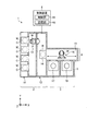
まず、実施形態に係る基板処理システム1(基板処理装置の一例)の構成について図1および図2を参照して説明する。図1は、実施形態に係る基板処理システム1を上方から見た模式的な断面図である。また、図2は、実施形態に係る基板処理システム1を側方から見た模式的な断面図である。なお、以下では、位置関係を明確にするために、互いに直交するX軸、Y軸およびZ軸を規定し、Z軸正方向を鉛直上向き方向とする。
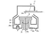
次に、液処理ユニット17の構成について、図3を参照しながら説明する。図3は、液処理ユニット17の構成例を示す図である。液処理ユニット17は、たとえば、スピン洗浄によりウェハWを1枚ずつ洗浄する枚葉式の洗浄装置として構成される。
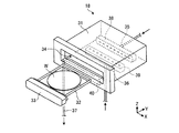
つづいて、乾燥ユニット18の構成について、図4を参照しながら説明する。図4は、乾燥ユニット18の構成例を示す模式斜視図である。
次に、上述した基板処理システム1におけるウェハWの処理フローについて、図5を参照しながら説明する。図5は、実施形態に係る基板処理システム1において実行される一連の基板処理の手順を示すフローチャートである。なお、図5に示す一連の基板処理は、制御部61の制御に従って実行される。
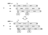
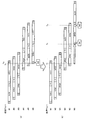
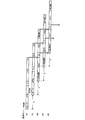
つづいて、第1搬送処理の開始タイミング設定処理の詳細について、図6〜図11を参照しながら説明する。図6〜図11は、実施形態に係る第1搬送処理の開始タイミング設定処理を説明するためのタイミングチャート(1)〜(6)である。なお、図6〜図11に示す第1搬送処理の開始タイミング設定処理は、制御部61の制御に従って実行される。
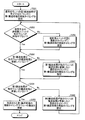
つづいて、実施形態に係る第1搬送処理の開始タイミング設定処理の手順について、図12を参照しながら説明する。図12は、実施形態に係る第1搬送処理の開始タイミング設定処理の手順を示すフローチャートである。
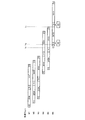
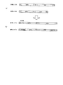
つづいては、実施形態の各種変形例について、図13〜図16を参照しながら説明する。図13は、実施形態の変形例1に係る第1搬送処理の開始タイミング設定処理の手順を説明するためのタイミングチャートである。なお、以下に示す各種変形例では、2組の液処理ユニット17および乾燥ユニット18がそれぞれペアになって連続的に基板処理を行う場合について示す。
1 基板処理システム(基板処理装置の一例)
14 受渡部
16 搬送装置(搬送部の一例)
17 液処理ユニット(第1処理部の一例)
18 乾燥ユニット(第2処理部の一例)
61 制御部
Claims (7)
- 基板に第1処理を施す複数の第1処理部と、
前記第1処理が施された前記基板に第2処理を施す複数の第2処理部と、
前記複数の第1処理部および前記複数の第2処理部に共通に前記基板を搬送する搬送部と、
前記複数の第1処理部、前記複数の第2処理部および前記搬送部を制御する制御部と、
を備え、
前記制御部は、
前記第1処理された後に液膜が形成された前記基板が前記第1処理部から前記第2処理部に搬送される第2搬送処理のタイミングと、他の前記基板が前記搬送部で搬送されるタイミングとが重複しないように、前記基板が前記第1処理部に搬送される第1搬送処理の開始タイミングを制御する
基板処理装置。 - 前記制御部は、前記基板の前記第1搬送処理および前記第2搬送処理のいずれもが、他の前記基板が前記搬送部で搬送されるタイミングと重複しない最前のタイミングに、前記基板の前記第1搬送処理の開始タイミングを設定する、請求項1に記載の基板処理装置。
- 前記制御部は、前記第1搬送処理の処理時間と、前記第1処理の処理時間と、前記第2搬送処理の処理時間と、前記第2処理の処理時間と、前記第2処理部から前記基板を搬出する第3搬送処理の処理時間とに基づいて、前記基板の前記第1搬送処理、前記第2搬送処理および前記第3搬送処理のタイミングと、他の前記基板が前記搬送部で搬送されるタイミングとが重複しない一定の間隔を算出し、
算出された一定の間隔ごとに前記第1搬送処理が開始されるように前記基板の前記第1搬送処理の開始タイミングを設定する、請求項1に記載の基板処理装置。 - 前記制御部は、前記基板に応じて異なる処理レシピがあらかじめ設定されている場合に、複数の前記第1処理および前記第2処理のうちもっとも長い処理時間に合わせるように、すべての前記処理レシピの前記第1処理の前に前待機処理を追加し、前記第2処理の後に後待機処理を追加する、請求項3に記載の基板処理装置。
- 前記第1処理は洗浄処理であり、前記第2処理は前記液膜が形成された前記基板を超臨界流体と接触させて前記基板を乾燥させる処理である、請求項1〜4のいずれか一つに記載の基板処理装置。
- 第1処理を施す複数の第1処理部のいずれか一つに基板を搬入する第1搬送処理と、
第2処理を施す複数の第2処理部のいずれか一つに前記第1処理部から前記基板を搬送する第2搬送処理と、
前記第2処理部から前記基板を搬出する第3搬送処理と、
を含み、
前記第1処理された後に液膜が形成された前記基板が前記第2搬送処理されるタイミングと、他の前記基板が搬送されるタイミングとが重複しないように、前記基板の前記第1搬送処理の開始タイミングを制御する
基板処理方法。 - 請求項6に記載の基板処理方法をコンピュータに実行させる、プログラムを記憶した記憶媒体。
Priority Applications (7)
| Application Number | Priority Date | Filing Date | Title |
|---|---|---|---|
| JP2018119628A JP7142494B2 (ja) | 2018-06-25 | 2018-06-25 | 基板処理装置および基板処理方法 |
| TW108121187A TWI800660B (zh) | 2018-06-25 | 2019-06-19 | 基板處理裝置及基板處理方法 |
| KR1020190073592A KR102678282B1 (ko) | 2018-06-25 | 2019-06-20 | 기판 처리 장치 및 기판 처리 방법 |
| US16/448,142 US11189481B2 (en) | 2018-06-25 | 2019-06-21 | Substrate processing apparatus and substrate processing method |
| CN201910554623.6A CN110634770B (zh) | 2018-06-25 | 2019-06-25 | 基板处理装置、基板处理方法以及存储介质 |
| CN202410867298.XA CN118866753A (zh) | 2018-06-25 | 2019-06-25 | 基板处理装置和基板处理方法 |
| KR1020240080081A KR102944346B1 (ko) | 2018-06-25 | 2024-06-20 | 기판 처리 장치 및 기판 처리 방법 |
Applications Claiming Priority (1)
| Application Number | Priority Date | Filing Date | Title |
|---|---|---|---|
| JP2018119628A JP7142494B2 (ja) | 2018-06-25 | 2018-06-25 | 基板処理装置および基板処理方法 |
Publications (2)
| Publication Number | Publication Date |
|---|---|
| JP2020004757A true JP2020004757A (ja) | 2020-01-09 |
| JP7142494B2 JP7142494B2 (ja) | 2022-09-27 |
Family
ID=68968808
Family Applications (1)
| Application Number | Title | Priority Date | Filing Date |
|---|---|---|---|
| JP2018119628A Active JP7142494B2 (ja) | 2018-06-25 | 2018-06-25 | 基板処理装置および基板処理方法 |
Country Status (5)
| Country | Link |
|---|---|
| US (1) | US11189481B2 (ja) |
| JP (1) | JP7142494B2 (ja) |
| KR (2) | KR102678282B1 (ja) |
| CN (2) | CN118866753A (ja) |
| TW (1) | TWI800660B (ja) |
Cited By (3)
| Publication number | Priority date | Publication date | Assignee | Title |
|---|---|---|---|---|
| JP2022151827A (ja) * | 2021-03-25 | 2022-10-07 | セメス カンパニー,リミテッド | 基板処理装置及び基板処理方法 |
| JP2023037608A (ja) * | 2021-09-03 | 2023-03-15 | セメス カンパニー,リミテッド | 基板処理装置及び方法 |
| JP2025074313A (ja) * | 2020-08-07 | 2025-05-13 | 東京エレクトロン株式会社 | 基板処理装置 |
Citations (3)
| Publication number | Priority date | Publication date | Assignee | Title |
|---|---|---|---|---|
| JPH07122622A (ja) * | 1993-07-15 | 1995-05-12 | Hitachi Ltd | 製造システムおよび製造方法 |
| WO2005112108A1 (ja) * | 2004-05-17 | 2005-11-24 | Hitachi Kokusai Electric Inc. | 基板処理装置及び半導体デバイス製造方法 |
| JP2017157746A (ja) * | 2016-03-03 | 2017-09-07 | 東京エレクトロン株式会社 | 基板処理装置、基板処理方法および記憶媒体 |
Family Cites Families (21)
| Publication number | Priority date | Publication date | Assignee | Title |
|---|---|---|---|---|
| JPH0722144B2 (ja) * | 1985-07-04 | 1995-03-08 | 株式会社東芝 | 半導体製造装置 |
| US5801945A (en) * | 1996-06-28 | 1998-09-01 | Lam Research Corporation | Scheduling method for robotic manufacturing processes |
| JP3668681B2 (ja) * | 1999-11-11 | 2005-07-06 | 東京エレクトロン株式会社 | 基板処理装置及び基板処理方法 |
| US7189647B2 (en) * | 2001-04-05 | 2007-03-13 | Novellus Systems, Inc. | Sequential station tool for wet processing of semiconductor wafers |
| US8078311B2 (en) * | 2004-12-06 | 2011-12-13 | Tokyo Electron Limited | Substrate processing apparatus and substrate transfer method adopted in substrate processing apparatus |
| US8015984B2 (en) * | 2005-06-22 | 2011-09-13 | Tokyo Electron Limited | Substrate processing apparatus including a drying mechanism using a fluid mixture of purified water and a volatile organic solvent |
| JP5427455B2 (ja) * | 2009-03-31 | 2014-02-26 | 大日本スクリーン製造株式会社 | 基板処理装置のスケジュール作成方法及びそのプログラム |
| JP5168300B2 (ja) * | 2010-02-24 | 2013-03-21 | 東京エレクトロン株式会社 | 基板処理装置及び基板処理方法 |
| WO2012147658A1 (ja) * | 2011-04-25 | 2012-11-01 | 株式会社ニコン | 基板処理装置 |
| JP5522124B2 (ja) | 2011-06-28 | 2014-06-18 | 東京エレクトロン株式会社 | 基板処理装置、基板処理方法および記憶媒体 |
| JP2013069874A (ja) * | 2011-09-22 | 2013-04-18 | Tokyo Electron Ltd | 基板処理システム、基板搬送方法、プログラム及びコンピュータ記憶媒体 |
| JP5632860B2 (ja) * | 2012-01-05 | 2014-11-26 | 東京エレクトロン株式会社 | 基板洗浄方法、基板洗浄装置及び基板洗浄用記憶媒体 |
| JP2013254904A (ja) * | 2012-06-08 | 2013-12-19 | Tokyo Electron Ltd | 基板処理装置及び基板処理方法 |
| JP2014082470A (ja) * | 2012-09-27 | 2014-05-08 | Ebara Corp | 基板処理装置 |
| JP6224359B2 (ja) * | 2013-06-20 | 2017-11-01 | 株式会社Screenホールディングス | 基板処理装置のためのスケジュール作成方法およびスケジュール作成プログラム |
| JP2015076433A (ja) * | 2013-10-07 | 2015-04-20 | 東京エレクトロン株式会社 | 基板搬送方法 |
| JP2015170833A (ja) * | 2014-03-11 | 2015-09-28 | 株式会社Screenホールディングス | 基板処理装置のスケジュール作成方法 |
| CN107851597B (zh) * | 2015-08-04 | 2021-10-01 | 株式会社国际电气 | 基板处理装置、半导体装置的制造方法及记录介质 |
| WO2017150038A1 (ja) * | 2016-03-03 | 2017-09-08 | 東京エレクトロン株式会社 | 基板処理装置、基板処理方法および記憶媒体 |
| JP6600588B2 (ja) * | 2016-03-17 | 2019-10-30 | 東京エレクトロン株式会社 | 基板搬送機構の洗浄方法及び基板処理システム |
| JP6320457B2 (ja) * | 2016-05-31 | 2018-05-09 | キヤノン株式会社 | 基板処理装置、基板処理方法、プログラム、及び物品製造方法 |
-
2018
- 2018-06-25 JP JP2018119628A patent/JP7142494B2/ja active Active
-
2019
- 2019-06-19 TW TW108121187A patent/TWI800660B/zh active
- 2019-06-20 KR KR1020190073592A patent/KR102678282B1/ko active Active
- 2019-06-21 US US16/448,142 patent/US11189481B2/en active Active
- 2019-06-25 CN CN202410867298.XA patent/CN118866753A/zh active Pending
- 2019-06-25 CN CN201910554623.6A patent/CN110634770B/zh active Active
-
2024
- 2024-06-20 KR KR1020240080081A patent/KR102944346B1/ko active Active
Patent Citations (3)
| Publication number | Priority date | Publication date | Assignee | Title |
|---|---|---|---|---|
| JPH07122622A (ja) * | 1993-07-15 | 1995-05-12 | Hitachi Ltd | 製造システムおよび製造方法 |
| WO2005112108A1 (ja) * | 2004-05-17 | 2005-11-24 | Hitachi Kokusai Electric Inc. | 基板処理装置及び半導体デバイス製造方法 |
| JP2017157746A (ja) * | 2016-03-03 | 2017-09-07 | 東京エレクトロン株式会社 | 基板処理装置、基板処理方法および記憶媒体 |
Cited By (7)
| Publication number | Priority date | Publication date | Assignee | Title |
|---|---|---|---|---|
| JP2025074313A (ja) * | 2020-08-07 | 2025-05-13 | 東京エレクトロン株式会社 | 基板処理装置 |
| JP2022151827A (ja) * | 2021-03-25 | 2022-10-07 | セメス カンパニー,リミテッド | 基板処理装置及び基板処理方法 |
| JP7344334B2 (ja) | 2021-03-25 | 2023-09-13 | セメス カンパニー,リミテッド | 基板処理装置及び基板処理方法 |
| US12325053B2 (en) | 2021-03-25 | 2025-06-10 | Semes Co., Ltd. | Substrate treating apparatus and substrate treating method |
| JP2023037608A (ja) * | 2021-09-03 | 2023-03-15 | セメス カンパニー,リミテッド | 基板処理装置及び方法 |
| JP7464665B2 (ja) | 2021-09-03 | 2024-04-09 | セメス カンパニー,リミテッド | 基板処理装置及び方法 |
| US12094706B2 (en) | 2021-09-03 | 2024-09-17 | Semes Co., Ltd. | Substrate treating apparatus and substrate treating method |
Also Published As
| Publication number | Publication date |
|---|---|
| KR20200000814A (ko) | 2020-01-03 |
| CN118866753A (zh) | 2024-10-29 |
| TW202014252A (zh) | 2020-04-16 |
| KR102678282B1 (ko) | 2024-06-25 |
| CN110634770B (zh) | 2024-07-16 |
| TWI800660B (zh) | 2023-05-01 |
| JP7142494B2 (ja) | 2022-09-27 |
| US11189481B2 (en) | 2021-11-30 |
| KR102944346B1 (ko) | 2026-03-27 |
| CN110634770A (zh) | 2019-12-31 |
| KR20240099123A (ko) | 2024-06-28 |
| US20190393028A1 (en) | 2019-12-26 |
Similar Documents
| Publication | Publication Date | Title |
|---|---|---|
| JP7113949B2 (ja) | 基板処理装置 | |
| KR102468102B1 (ko) | 기판 처리 장치 | |
| KR102944346B1 (ko) | 기판 처리 장치 및 기판 처리 방법 | |
| JP2023001153A (ja) | 基板処理システム | |
| JP2020017618A (ja) | 基板処理装置および基板処理方法 | |
| JP2018207076A (ja) | 基板処理装置 | |
| US12412766B2 (en) | Substrate processing apparatus and substrate processing method | |
| JP7562913B2 (ja) | 基板処理方法および基板処理装置 | |
| KR20230168139A (ko) | 기판 처리 장치 및 기판 처리 방법 | |
| KR20190060674A (ko) | 기판 처리 방법 및 기판 처리 장치 |
Legal Events
| Date | Code | Title | Description |
|---|---|---|---|
| A621 | Written request for application examination |
Free format text: JAPANESE INTERMEDIATE CODE: A621 Effective date: 20210413 |
|
| A977 | Report on retrieval |
Free format text: JAPANESE INTERMEDIATE CODE: A971007 Effective date: 20220516 |
|
| A131 | Notification of reasons for refusal |
Free format text: JAPANESE INTERMEDIATE CODE: A131 Effective date: 20220614 |
|
| A521 | Request for written amendment filed |
Free format text: JAPANESE INTERMEDIATE CODE: A523 Effective date: 20220720 |
|
| TRDD | Decision of grant or rejection written | ||
| A01 | Written decision to grant a patent or to grant a registration (utility model) |
Free format text: JAPANESE INTERMEDIATE CODE: A01 Effective date: 20220816 |
|
| A61 | First payment of annual fees (during grant procedure) |
Free format text: JAPANESE INTERMEDIATE CODE: A61 Effective date: 20220913 |
|
| R150 | Certificate of patent or registration of utility model |
Ref document number: 7142494 Country of ref document: JP Free format text: JAPANESE INTERMEDIATE CODE: R150 |
|
| R250 | Receipt of annual fees |
Free format text: JAPANESE INTERMEDIATE CODE: R250 |