JP2020008710A - マッハツェンダー変調器、マッハツェンダー変調器を作製する方法 - Google Patents
マッハツェンダー変調器、マッハツェンダー変調器を作製する方法 Download PDFInfo
- Publication number
- JP2020008710A JP2020008710A JP2018129243A JP2018129243A JP2020008710A JP 2020008710 A JP2020008710 A JP 2020008710A JP 2018129243 A JP2018129243 A JP 2018129243A JP 2018129243 A JP2018129243 A JP 2018129243A JP 2020008710 A JP2020008710 A JP 2020008710A
- Authority
- JP
- Japan
- Prior art keywords
- resin body
- mach
- mesa
- waveguide
- zehnder modulator
- Prior art date
- Legal status (The legal status is an assumption and is not a legal conclusion. Google has not performed a legal analysis and makes no representation as to the accuracy of the status listed.)
- Granted
Links
Images



Classifications
-
- G—PHYSICS
- G02—OPTICS
- G02F—OPTICAL DEVICES OR ARRANGEMENTS FOR THE CONTROL OF LIGHT BY MODIFICATION OF THE OPTICAL PROPERTIES OF THE MEDIA OF THE ELEMENTS INVOLVED THEREIN; NON-LINEAR OPTICS; FREQUENCY-CHANGING OF LIGHT; OPTICAL LOGIC ELEMENTS; OPTICAL ANALOGUE/DIGITAL CONVERTERS
- G02F1/00—Devices or arrangements for the control of the intensity, colour, phase, polarisation or direction of light arriving from an independent light source, e.g. switching, gating or modulating; Non-linear optics
- G02F1/01—Devices or arrangements for the control of the intensity, colour, phase, polarisation or direction of light arriving from an independent light source, e.g. switching, gating or modulating; Non-linear optics for the control of the intensity, phase, polarisation or colour
- G02F1/21—Devices or arrangements for the control of the intensity, colour, phase, polarisation or direction of light arriving from an independent light source, e.g. switching, gating or modulating; Non-linear optics for the control of the intensity, phase, polarisation or colour by interference
- G02F1/225—Devices or arrangements for the control of the intensity, colour, phase, polarisation or direction of light arriving from an independent light source, e.g. switching, gating or modulating; Non-linear optics for the control of the intensity, phase, polarisation or colour by interference in an optical waveguide structure
- G02F1/2257—Devices or arrangements for the control of the intensity, colour, phase, polarisation or direction of light arriving from an independent light source, e.g. switching, gating or modulating; Non-linear optics for the control of the intensity, phase, polarisation or colour by interference in an optical waveguide structure the optical waveguides being made of semiconducting material
-
- G—PHYSICS
- G02—OPTICS
- G02F—OPTICAL DEVICES OR ARRANGEMENTS FOR THE CONTROL OF LIGHT BY MODIFICATION OF THE OPTICAL PROPERTIES OF THE MEDIA OF THE ELEMENTS INVOLVED THEREIN; NON-LINEAR OPTICS; FREQUENCY-CHANGING OF LIGHT; OPTICAL LOGIC ELEMENTS; OPTICAL ANALOGUE/DIGITAL CONVERTERS
- G02F1/00—Devices or arrangements for the control of the intensity, colour, phase, polarisation or direction of light arriving from an independent light source, e.g. switching, gating or modulating; Non-linear optics
- G02F1/01—Devices or arrangements for the control of the intensity, colour, phase, polarisation or direction of light arriving from an independent light source, e.g. switching, gating or modulating; Non-linear optics for the control of the intensity, phase, polarisation or colour
- G02F1/21—Devices or arrangements for the control of the intensity, colour, phase, polarisation or direction of light arriving from an independent light source, e.g. switching, gating or modulating; Non-linear optics for the control of the intensity, phase, polarisation or colour by interference
- G02F1/212—Mach-Zehnder type
Landscapes
- Physics & Mathematics (AREA)
- Nonlinear Science (AREA)
- General Physics & Mathematics (AREA)
- Optics & Photonics (AREA)
- Optical Modulation, Optical Deflection, Nonlinear Optics, Optical Demodulation, Optical Logic Elements (AREA)
Abstract
Description
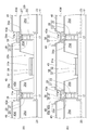
導波路メサ17の一例。
基板11:半絶縁性InP。
下部クラッド層17a:n型InP。
コア層17b:AlGaInAs量子井戸。
上部クラッド層17c:p型InP。
コンタクト層17d:p型InGaAs。
下部クラッド層17a、コア層17b、上部クラッド層17c及びコンタクト層17dは、基板11の主面11a上に順に配列される。
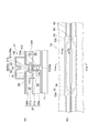
第2オーミック電極35aは、導波路メサ17の上面17eの全体を覆う上部分35bと、導波路メサ17の側面17fに接触を成す側部分35cとを有することができる。第2オーミック電極35aの側部分35cは、無機絶縁体領域29によって第1埋込樹脂体25dから隔置される。第2オーミック電極35aに側部分35cに設けることによって、導波路メサ17の上面17eの全体に接触を成す上部分35bを第2オーミック電極35aに提供できる。
Claims (6)
- マッハツェンダー変調器を作製する方法であって、
基板上に設けられた導波路メサと、前記導波路メサの側面を埋め込む埋込樹脂体と、前記導波路メサから隔置されるように前記埋込樹脂体を覆うと共に前記導波路メサの上面及び前記側面を覆う無機絶縁体とを含む基板生産物を準備する工程と、
前記無機絶縁体をエッチングして、前記導波路メサの前記上面に至る開口を有すると共に前記導波路メサの前記側面及び前記埋込樹脂体を覆う無機絶縁体領域を形成する工程と、
前記無機絶縁体領域の前記開口にオーミック電極を形成する工程と、
を備え、
前記オーミック電極は、前記埋込樹脂体から隔置されると共に、前記導波路メサの前記上面に接触を成す、マッハツェンダー変調器を作製する方法。 - 前記無機絶縁体領域の前記開口は、前記導波路メサの前記上面の幅より大きい幅を有する、請求項1に記載されたマッハツェンダー変調器を作製する方法。
- 前記オーミック電極は、前記導波路メサの前記上面の全体を覆う上部分と、前記導波路メサの前記側面に接触を成す側部分とを有し、
前記オーミック電極の前記側部分は、前記無機絶縁体領域によって前記埋込樹脂体から隔置される、請求項1又は請求項2に記載されたマッハツェンダー変調器を作製する方法。 - マッハツェンダー変調器であって、
側面及び上面を有する半導体アーム導波路構造と、
前記半導体アーム導波路構造を埋め込む埋込樹脂体と、
前記半導体アーム導波路構造の前記上面に到達する開口を有すると共に前記半導体アーム導波路構造の前記側面及び前記埋込樹脂体を覆う無機絶縁体領域と、
前記無機絶縁体領域の前記開口を介して前記半導体アーム導波路構造の前記上面に接触を成す電極と、
を備える、マッハツェンダー変調器。 - 前記無機絶縁体領域の前記開口は、前記半導体アーム導波路構造の前記上面の幅より大きい幅を有する、請求項4に記載されたマッハツェンダー変調器。
- 前記電極はオーミック電極を含み、
前記オーミック電極は、前記半導体アーム導波路構造の前記上面の全体を覆うと共に前記埋込樹脂体から隔置される、請求項4又は請求項5に記載されたマッハツェンダー変調器。
Priority Applications (2)
| Application Number | Priority Date | Filing Date | Title |
|---|---|---|---|
| JP2018129243A JP7077824B2 (ja) | 2018-07-06 | 2018-07-06 | マッハツェンダー変調器を作製する方法 |
| US16/502,098 US10901290B2 (en) | 2018-07-06 | 2019-07-03 | Method for fabricating Mach-Zehnder modulator, Mach-Zehnder modulator |
Applications Claiming Priority (1)
| Application Number | Priority Date | Filing Date | Title |
|---|---|---|---|
| JP2018129243A JP7077824B2 (ja) | 2018-07-06 | 2018-07-06 | マッハツェンダー変調器を作製する方法 |
Publications (2)
| Publication Number | Publication Date |
|---|---|
| JP2020008710A true JP2020008710A (ja) | 2020-01-16 |
| JP7077824B2 JP7077824B2 (ja) | 2022-05-31 |
Family
ID=69102010
Family Applications (1)
| Application Number | Title | Priority Date | Filing Date |
|---|---|---|---|
| JP2018129243A Active JP7077824B2 (ja) | 2018-07-06 | 2018-07-06 | マッハツェンダー変調器を作製する方法 |
Country Status (2)
| Country | Link |
|---|---|
| US (1) | US10901290B2 (ja) |
| JP (1) | JP7077824B2 (ja) |
Families Citing this family (1)
| Publication number | Priority date | Publication date | Assignee | Title |
|---|---|---|---|---|
| JP2024110338A (ja) * | 2023-02-02 | 2024-08-15 | 富士通オプティカルコンポーネンツ株式会社 | 光デバイス、光送受信器及び光トランシーバ |
Citations (8)
| Publication number | Priority date | Publication date | Assignee | Title |
|---|---|---|---|---|
| JPH07211982A (ja) * | 1994-01-20 | 1995-08-11 | Matsushita Electron Corp | 半導体発光装置 |
| US20070223543A1 (en) * | 2004-05-20 | 2007-09-27 | Kelvin Prosyk | Laterally Implanted Electroabsorption Modulated Laser |
| JP2007311591A (ja) * | 2006-05-19 | 2007-11-29 | Matsushita Electric Ind Co Ltd | 窒化物半導体レーザ装置及びその製造方法 |
| JP2011022281A (ja) * | 2009-07-14 | 2011-02-03 | Fujitsu Ltd | 半導体装置及びその製造方法 |
| JP2011247926A (ja) * | 2010-05-24 | 2011-12-08 | Fujitsu Ltd | マッハツェンダ型変調器の制御方法及び光モジュール |
| JP2012123184A (ja) * | 2010-12-08 | 2012-06-28 | Sumitomo Electric Ind Ltd | 半導体光変調素子及びその製造方法 |
| JP2018097199A (ja) * | 2016-12-14 | 2018-06-21 | 住友電気工業株式会社 | 半導体素子及び半導体素子の製造方法 |
| WO2019026943A1 (ja) * | 2017-08-01 | 2019-02-07 | 三菱電機株式会社 | 光半導体素子の製造方法および光半導体素子 |
Family Cites Families (8)
| Publication number | Priority date | Publication date | Assignee | Title |
|---|---|---|---|---|
| JP2002232004A (ja) | 2001-01-31 | 2002-08-16 | Kyocera Corp | Ledアレイ |
| JP5418887B2 (ja) * | 2009-05-27 | 2014-02-19 | 住友電気工業株式会社 | 半導体レーザ素子の製造方法及び半導体レーザ素子 |
| JP5678528B2 (ja) | 2010-09-07 | 2015-03-04 | 住友電気工業株式会社 | 半導体光デバイスの製造方法 |
| JP5767864B2 (ja) | 2011-06-07 | 2015-08-26 | 日本オクラロ株式会社 | 光素子、光素子を含む変調器モジュール、光素子を含むレーザ集積変調器モジュール、及び、光素子の製造方法 |
| JP5795970B2 (ja) | 2012-03-01 | 2015-10-14 | Nttエレクトロニクス株式会社 | ボンディングパッド電極形成方法 |
| JP6236947B2 (ja) * | 2013-07-16 | 2017-11-29 | 住友電気工業株式会社 | 半導体光素子を製造する方法、および半導体光素子 |
| JP6394454B2 (ja) * | 2015-03-24 | 2018-09-26 | 住友電気工業株式会社 | マッハツェンダー変調器 |
| JP6862983B2 (ja) * | 2017-03-23 | 2021-04-21 | 住友電気工業株式会社 | 半導体光素子及びその製造方法 |
-
2018
- 2018-07-06 JP JP2018129243A patent/JP7077824B2/ja active Active
-
2019
- 2019-07-03 US US16/502,098 patent/US10901290B2/en active Active
Patent Citations (8)
| Publication number | Priority date | Publication date | Assignee | Title |
|---|---|---|---|---|
| JPH07211982A (ja) * | 1994-01-20 | 1995-08-11 | Matsushita Electron Corp | 半導体発光装置 |
| US20070223543A1 (en) * | 2004-05-20 | 2007-09-27 | Kelvin Prosyk | Laterally Implanted Electroabsorption Modulated Laser |
| JP2007311591A (ja) * | 2006-05-19 | 2007-11-29 | Matsushita Electric Ind Co Ltd | 窒化物半導体レーザ装置及びその製造方法 |
| JP2011022281A (ja) * | 2009-07-14 | 2011-02-03 | Fujitsu Ltd | 半導体装置及びその製造方法 |
| JP2011247926A (ja) * | 2010-05-24 | 2011-12-08 | Fujitsu Ltd | マッハツェンダ型変調器の制御方法及び光モジュール |
| JP2012123184A (ja) * | 2010-12-08 | 2012-06-28 | Sumitomo Electric Ind Ltd | 半導体光変調素子及びその製造方法 |
| JP2018097199A (ja) * | 2016-12-14 | 2018-06-21 | 住友電気工業株式会社 | 半導体素子及び半導体素子の製造方法 |
| WO2019026943A1 (ja) * | 2017-08-01 | 2019-02-07 | 三菱電機株式会社 | 光半導体素子の製造方法および光半導体素子 |
Also Published As
| Publication number | Publication date |
|---|---|
| US20200012164A1 (en) | 2020-01-09 |
| US10901290B2 (en) | 2021-01-26 |
| JP7077824B2 (ja) | 2022-05-31 |
Similar Documents
| Publication | Publication Date | Title |
|---|---|---|
| JP5942785B2 (ja) | 半導体光素子を作製する方法 | |
| KR100278214B1 (ko) | 연장하는포토레지스트층으로패턴상이정확히전사되도록하는트렌치분리부를갖는반도체장치의제조방법 | |
| JP6326722B2 (ja) | マッハツェンダ変調器を作製する方法 | |
| US10754093B2 (en) | Fabrication process of polymer based photonic apparatus and the apparatus | |
| JP7077824B2 (ja) | マッハツェンダー変調器を作製する方法 | |
| US20200144111A1 (en) | Metal interconnection structure and method for fabricating same | |
| KR100253394B1 (ko) | 듀얼 게이트절연막을 가지는 게이트전극의 제조방법 | |
| JP6773260B1 (ja) | 半導体装置及びその製造方法 | |
| JPWO2019026943A1 (ja) | 光半導体素子の製造方法および光半導体素子 | |
| JP6589530B2 (ja) | 半導体光素子を作製する方法、半導体光素子 | |
| JP2013044803A (ja) | 光半導体素子の製造方法 | |
| KR100225955B1 (ko) | 반도체 소자의 소자분리막 형성방법 | |
| JPH05267448A (ja) | 半導体装置の素子分離方法 | |
| JP6690457B2 (ja) | マッハツェンダー変調器を作製する方法、マッハツェンダー変調器 | |
| JP4226115B2 (ja) | 半導体素子のマスク製造方法 | |
| CN113300217A (zh) | 一种基于掩埋金属掩膜的脊表面光栅制作方法 | |
| JP7020155B2 (ja) | マッハツェンダ変調器を作製する方法、マッハツェンダ変調器 | |
| US20240170559A1 (en) | Method for producing closely spaced gate structures of a quantum dot device | |
| JPH033936B2 (ja) | ||
| JP2892122B2 (ja) | 半導体レーザの製造方法 | |
| JPH02254720A (ja) | 微細エッチング方法 | |
| KR0157888B1 (ko) | 반도체 장치의 소자분리방법 | |
| JP2981347B2 (ja) | 半導体素子の製造方法 | |
| WO2024209538A1 (ja) | 半導体装置の製造方法 | |
| JPH0897461A (ja) | 半導体受光素子,及びその製造方法 |
Legal Events
| Date | Code | Title | Description |
|---|---|---|---|
| A621 | Written request for application examination |
Free format text: JAPANESE INTERMEDIATE CODE: A621 Effective date: 20201221 |
|
| A977 | Report on retrieval |
Free format text: JAPANESE INTERMEDIATE CODE: A971007 Effective date: 20211126 |
|
| A131 | Notification of reasons for refusal |
Free format text: JAPANESE INTERMEDIATE CODE: A131 Effective date: 20211130 |
|
| A521 | Request for written amendment filed |
Free format text: JAPANESE INTERMEDIATE CODE: A523 Effective date: 20211216 |
|
| TRDD | Decision of grant or rejection written | ||
| A01 | Written decision to grant a patent or to grant a registration (utility model) |
Free format text: JAPANESE INTERMEDIATE CODE: A01 Effective date: 20220419 |
|
| A61 | First payment of annual fees (during grant procedure) |
Free format text: JAPANESE INTERMEDIATE CODE: A61 Effective date: 20220502 |
|
| R150 | Certificate of patent or registration of utility model |
Ref document number: 7077824 Country of ref document: JP Free format text: JAPANESE INTERMEDIATE CODE: R150 |
|
| R250 | Receipt of annual fees |
Free format text: JAPANESE INTERMEDIATE CODE: R250 |
|
| R250 | Receipt of annual fees |
Free format text: JAPANESE INTERMEDIATE CODE: R250 |