JP2020101460A - Film thickness measuring apparatus and film thickness measuring method of silicon epitaxial layer in epitaxial silicon wafer with embedded diffusion layer, and manufacturing method of epitaxial silicon wafer with embedded diffusion layer using film thickness measuring apparatus or film thickness measuring method - Google Patents
Film thickness measuring apparatus and film thickness measuring method of silicon epitaxial layer in epitaxial silicon wafer with embedded diffusion layer, and manufacturing method of epitaxial silicon wafer with embedded diffusion layer using film thickness measuring apparatus or film thickness measuring method Download PDFInfo
- Publication number
- JP2020101460A JP2020101460A JP2018240172A JP2018240172A JP2020101460A JP 2020101460 A JP2020101460 A JP 2020101460A JP 2018240172 A JP2018240172 A JP 2018240172A JP 2018240172 A JP2018240172 A JP 2018240172A JP 2020101460 A JP2020101460 A JP 2020101460A
- Authority
- JP
- Japan
- Prior art keywords
- film thickness
- silicon
- diffusion layer
- layer
- epitaxial
- Prior art date
- Legal status (The legal status is an assumption and is not a legal conclusion. Google has not performed a legal analysis and makes no representation as to the accuracy of the status listed.)
- Granted
Links
Images
Landscapes
- Length Measuring Devices By Optical Means (AREA)
- Testing Or Measuring Of Semiconductors Or The Like (AREA)
Abstract
【課題】シリコン基板のドーパント濃度が低い埋込み拡散層付きエピタキシャルシリコンウェーハであっても、シリコンエピタキシャル層の膜厚を高精度に測定することが可能な膜厚測定装置を提供する。【解決手段】本発明の膜厚測定装置1は、赤外光源2と、赤外光から干渉光Lを生成する干渉計3と、埋込み拡散層付きエピタキシャルシリコンウェーハWを載置する測定ステージ6と、干渉光Lがシリコンエピタキシャル層18の表面で反射して生じた反射光R1と、干渉光Lがシリコンエピタキシャル層18と埋込み拡散層16の界面で反射して生じた反射光R2を検出する検出器5と、検出器5の出力からシリコンエピタキシャル層18の膜厚を算出する制御部と、を備え、測定ステージ6は、赤外光のスペクトルのピーク波長での反射率が15%以下である材質からなる。【選択図】図1PROBLEM TO BE SOLVED: To provide a film thickness measuring device capable of measuring the film thickness of a silicon epitaxial layer with high accuracy even in an epitaxial silicon wafer with an embedded diffusion layer having a low dopant concentration of a silicon substrate. A film thickness measuring device 1 of the present invention mounts an infrared light source 2, an interferometer 3 that generates interference light L from infrared light, and an epitaxial silicon wafer W with an embedded diffusion layer. The reflected light R1 generated by the interference light L reflected on the surface of the silicon epitaxial layer 18 and the reflected light R2 generated by the interference light L reflected at the interface between the silicon epitaxial layer 18 and the embedded diffusion layer 16 are detected. A detector 5 and a control unit for calculating the thickness of the silicon epitaxial layer 18 from the output of the detector 5 are provided, and the measurement stage 6 has a reflectance of 15% or less at the peak wavelength of the infrared light spectrum. It is made of a certain material. [Selection diagram] Fig. 1
Description
本発明は、埋込み拡散層付きエピタキシャルシリコンウェーハにおけるシリコンエピタキシャル層の膜厚測定装置および膜厚測定方法、ならびに当該膜厚測定装置または当該膜厚測定方法を用いたエピタキシャルシリコンウェーハの製造方法に関する。 The present invention relates to a film thickness measuring device and a film thickness measuring method for a silicon epitaxial layer in an epitaxial silicon wafer with a buried diffusion layer, and a method for manufacturing an epitaxial silicon wafer using the film thickness measuring device or the film thickness measuring method.
シリコン基板の表層に集積回路用の埋込み拡散層を形成し、当該埋込み拡散層上にシリコンエピタキシャル層などの単結晶薄膜を形成したシリコンウェーハがある。特許文献1では、このように埋込み拡散層が形成されたシリコンウェーハにおける単結晶薄膜の膜厚をフーリエ変換赤外分光計(FTIR:Fourier transform infrared spectrometer)により測定する方法が提案されている。 There is a silicon wafer in which a buried diffusion layer for an integrated circuit is formed on the surface layer of a silicon substrate, and a single crystal thin film such as a silicon epitaxial layer is formed on the buried diffusion layer. Patent Document 1 proposes a method of measuring the film thickness of a single crystal thin film on a silicon wafer on which a buried diffusion layer is formed by a Fourier transform infrared spectrometer (FTIR).
すなわち、光源から出射した赤外光から干渉光を生成し、この干渉光をシリコンウェーハに照射する。そして、この干渉光が単結晶薄膜の表面で反射することによって生じた第1の反射光を検出器で検出する。これと同時に、この干渉光が、単結晶薄膜を透過し、単結晶薄膜と埋込み拡散層との界面で反射することによって生じた第2の反射光を検出器で検出する。そして、検出器で検出した第1の反射光と第2の反射光のインタフェログラムに対して、余弦フーリエ変換および逆変換を施して第1の曲線を得る。また、同インタフェログラムに対して正弦フーリエ変換および逆変換を施して第2の曲線を得る。そして、第1の曲線と第2の曲線を合成して得られる合成曲線における複数のピークのうち、反射光の光路差の絶対値が最小となるピークから単結晶薄膜の膜厚を算出する。 That is, the interference light is generated from the infrared light emitted from the light source, and the silicon wafer is irradiated with the interference light. Then, the detector detects the first reflected light generated by reflecting the interference light on the surface of the single crystal thin film. At the same time, the interference light is transmitted through the single crystal thin film and is reflected by the interface between the single crystal thin film and the buried diffusion layer, whereby the second reflected light is detected by the detector. Then, a cosine Fourier transform and an inverse transform are applied to the interferogram of the first reflected light and the second reflected light detected by the detector to obtain the first curve. Also, the same interferogram is subjected to sine Fourier transform and inverse transform to obtain a second curve. Then, the film thickness of the single crystal thin film is calculated from the peak having the minimum absolute value of the optical path difference of the reflected light among the plurality of peaks in the combined curve obtained by combining the first curve and the second curve.
埋込み拡散層を有し、かつ単結晶薄膜としてシリコンエピタキシャル層を有する埋込み拡散層付きエピタキシャルシリコンウェーハを高耐圧のパワーデバイス用ウェーハとして用いる場合、シリコン基板のドーパント濃度は、一般に2.8×10¹⁷atoms/cm3超(p型の場合)と高く設定される。一方で、例えばBi−CMOS用のウェーハとして、埋込み拡散層付きエピタキシャルシリコンウェーハを用いる場合、シリコン基板のドーパント濃度は、一般に2.8×1017atoms/cm3以下(p型の場合)と低く設定される。前者の埋込み拡散層付きエピタキシャルシリコンウェーハにおけるシリコンエピタキシャル層の膜厚は、特許文献1に記載の測定方法でも正確に測定することができる。ところが、本発明者らは、後者の埋込み拡散層付きエピタキシャルシリコンウェーハにおけるシリコンエピタキシャル層の膜厚を特許文献1に記載の方法で測定しても、正確に測定することができないという新規な課題を認識した。 When an epitaxial silicon wafer with a buried diffusion layer having a buried diffusion layer and a silicon epitaxial layer as a single crystal thin film is used as a wafer for a high-voltage power device, the dopant concentration of the silicon substrate is generally 2.8×10 17. It is set as high as over atoms/cm 3 (for p-type). On the other hand, when an epitaxial silicon wafer with a buried diffusion layer is used as a wafer for Bi-CMOS, for example, the dopant concentration of the silicon substrate is generally as low as 2.8×10 17 atoms/cm 3 (in the case of p type). Is set. The film thickness of the silicon epitaxial layer in the former epitaxial silicon wafer with a buried diffusion layer can be accurately measured by the measuring method described in Patent Document 1. However, the inventors of the present invention have a new problem that even if the film thickness of the silicon epitaxial layer in the latter epitaxial silicon wafer with a buried diffusion layer is measured by the method described in Patent Document 1, it cannot be accurately measured. I recognized.
本発明は、上記課題に鑑み、シリコン基板のドーパント濃度が低い埋込み拡散層付きエピタキシャルシリコンウェーハであっても、シリコンエピタキシャル層の膜厚を高精度に測定することが可能な膜厚測定装置および膜厚測定方法を提供することを目的とする。また、本発明は、当該膜厚測定装置または当該膜厚測定方法によって得ることが可能な埋込み拡散層付きエピタキシャルシリコンウェーハの製造方法を提供することを目的とする。 In view of the above problems, the present invention provides a film thickness measuring device and a film capable of measuring the film thickness of a silicon epitaxial layer with high accuracy even in an epitaxial silicon wafer with a buried diffusion layer having a low dopant concentration in a silicon substrate. It is intended to provide a thickness measuring method. Another object of the present invention is to provide a method for manufacturing an epitaxial silicon wafer with a buried diffusion layer, which can be obtained by the film thickness measuring device or the film thickness measuring method.
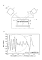
埋込み拡散層付きエピタキシャルシリコンウェーハにおけるシリコンエピタキシャル層の膜厚は、例えば図3(A)に示す膜厚測定装置1を用いて測定することができる。すなわち、光源2から出射した赤外線は、干渉計3により干渉光L,L’となって、測定ステージ7に載置されたエピタキシャルシリコンウェーハWに入射する。そして、干渉光Lがシリコンエピタキシャル層18の表面で反射することによって生じた第1の反射光R1が検出器5に入射する。これと同時に、干渉光Lが、シリコンエピタキシャル層18を透過し、シリコンエピタキシャル層18と埋込み拡散層16の界面で反射することによって生じた第2の反射光R2も検出器5に入射して、これらの反射光を検出器5で検出する。そして、制御部(不図示)が検出器5からの出力である第1の反射光R1と第2の反射光R2のインタフェログラムを解析することによって、シリコンエピタキシャル層18の膜厚を算出する。
The film thickness of the silicon epitaxial layer in the epitaxial silicon wafer with the embedded diffusion layer can be measured using, for example, the film thickness measuring device 1 shown in FIG. That is, the infrared light emitted from the
本発明者らは、シリコン基板10のドーパント濃度が低い埋込み拡散層付きエピタキシャルシリコンウェーハWにおける干渉光の状態を検討した。すると、干渉光L’に起因する第3の反射光R3が存在することが判明した。そして、この第3の反射光R3がシリコンエピタキシャル層18の膜厚の測定に悪影響を及ぼすことがわかった。すなわち、図3(A)に示すように、干渉光L’は、シリコンエピタキシャル層18を透過した後に、シリコン基板10の表層のうち埋込み拡散層16が存在しない領域を透過し、埋込み拡散層付きエピタキシャルシリコンウェーハWと測定ステージ6との界面で反射して、第3の反射光R3となる。この第3の反射光R3は、図3(B)に示すように、第1の反射光R1と第2の反射光R2のインタフェログラムにノイズを発生させ、これに起因してシリコンエピタキシャル層18の膜厚が誤って算出される。一方で、シリコン基板10のドーパント濃度が高い場合には、干渉光L’がシリコン基板10を透過しないので、上記の問題が生じないことがわかった。そして、さらなる検討を進めたところ、赤外光の反射率を考慮して、測定ステージ6の材質を選択することにより、インタフェログラムにおけるノイズを低減することができ、その結果、シリコンエピタキシャル層18の膜厚を高精度に測定することができることを知見した。
The present inventors have examined the state of interference light in the epitaxial silicon wafer W with a buried diffusion layer in which the dopant concentration of the
本発明は、上記知見に基づいて完成されたものであり、その要旨構成は以下のとおりである。
(1)シリコン基板と、前記シリコン基板の表層に形成された埋込み拡散層と、前記埋込み拡散層上に形成されたシリコンエピタキシャル層と、を有する埋込み拡散層付きエピタキシャルシリコンウェーハにおける前記シリコンエピタキシャル層の膜厚を測定するための膜厚測定装置であって、
赤外光を出射する光源と、
前記赤外光の光路上に配置され、かつ、前記赤外光から、前記埋込み拡散層付きエピタキシャルシリコンウェーハに照射するための干渉光を生成する干渉計と、
前記干渉光の光路上に前記埋込み拡散層付きエピタキシャルシリコンウェーハが位置するように、前記埋込み拡散層付きエピタキシャルシリコンウェーハを載置するための測定ステージと、
前記干渉光が前記シリコンエピタキシャル層の表面で反射することによって生じる第1の反射光と、前記干渉光が前記シリコンエピタキシャル層を透過して、前記シリコンエピタキシャル層と前記埋込み拡散層との界面で反射することによって生じる第2の反射光と、の光路上に配置され、かつ、前記第1の反射光と前記第2の反射光を検出する検出器と、
前記検出器の出力に基づき、前記シリコンエピタキシャル層の膜厚を算出する制御部と、
を備え、
前記測定ステージは、前記赤外光のスペクトルのピーク波長における反射率が15%以下である材質からなることを特徴とする膜厚測定装置。
The present invention has been completed based on the above findings, and its gist configuration is as follows.
(1) Of the silicon epitaxial layer in an epitaxial silicon wafer with a buried diffusion layer, which includes a silicon substrate, a buried diffusion layer formed on a surface layer of the silicon substrate, and a silicon epitaxial layer formed on the buried diffusion layer. A film thickness measuring device for measuring the film thickness,
A light source that emits infrared light,
Arranged on the optical path of the infrared light, and, from the infrared light, an interferometer for generating interference light for irradiating the epitaxial silicon wafer with the buried diffusion layer,
The measurement stage for mounting the epitaxial silicon wafer with the buried diffusion layer so that the buried diffusion layer with the epitaxial silicon wafer is located on the optical path of the interference light,
First reflected light generated by the interference light being reflected on the surface of the silicon epitaxial layer, and the interference light being transmitted through the silicon epitaxial layer and reflected at the interface between the silicon epitaxial layer and the buried diffusion layer. A detector that is disposed on the optical path of the second reflected light generated by the above, and that detects the first reflected light and the second reflected light;
A control unit for calculating the film thickness of the silicon epitaxial layer based on the output of the detector;
Equipped with
The film thickness measuring device, wherein the measuring stage is made of a material having a reflectance of 15% or less at a peak wavelength of the spectrum of the infrared light.
(2)前記測定ステージは、石英、フッ素樹脂、及びセラミックスのうちから選択される1つ以上の材質からなる、上記(1)に記載の膜厚測定装置。 (2) The film thickness measuring device according to (1), wherein the measuring stage is made of one or more materials selected from quartz, fluororesin, and ceramics.
(3)前記測定ステージは、ウェーハ搬送用エンドエフェクタにおけるウェーハ保持部である、上記(1)または(2)に記載の膜厚測定装置。 (3) The film thickness measuring device as described in (1) or (2) above, wherein the measurement stage is a wafer holding part in a wafer transfer end effector.
(4)シリコン基板と、前記シリコン基板の表層に形成された埋込み拡散層と、前記埋込み拡散層上に形成されたシリコンエピタキシャル層と、を有する埋込み拡散層付きエピタキシャルシリコンウェーハにおける前記シリコンエピタキシャル層の膜厚を測定するための膜厚測定方法であって、
赤外光から干渉光を生成し、
測定ステージに載置された前記埋込み拡散層付きエピタキシャルシリコンウェーハに、前記干渉光を照射し、
前記干渉光が前記シリコンエピタキシャル層の表面で反射することによって生じる第1の反射光と、前記干渉光が前記シリコンエピタキシャル層を透過して、前記シリコンエピタキシャル層と前記埋込み拡散層との界面で反射することによって生じる第2の反射光とを検出し、
前記シリコンエピタキシャル層の膜厚を算出し、
前記測定ステージは、前記赤外光のスペクトルのピーク波長における反射率が15%以下である材質からなることを特徴とする膜厚測定方法。
(4) Of the silicon epitaxial layer in an epitaxial silicon wafer with a buried diffusion layer, which comprises a silicon substrate, a buried diffusion layer formed on a surface layer of the silicon substrate, and a silicon epitaxial layer formed on the buried diffusion layer. A film thickness measuring method for measuring the film thickness,
Generates interference light from infrared light,
Irradiating the interference light to the epitaxial silicon wafer with the embedded diffusion layer placed on the measurement stage,
First reflected light generated by the interference light being reflected on the surface of the silicon epitaxial layer, and the interference light being transmitted through the silicon epitaxial layer and reflected at the interface between the silicon epitaxial layer and the buried diffusion layer. Detecting the second reflected light generated by
Calculate the film thickness of the silicon epitaxial layer,
The film thickness measuring method, wherein the measuring stage is made of a material having a reflectance of 15% or less at a peak wavelength of the spectrum of infrared light.
(5)前記測定ステージは、石英、フッ素樹脂、及びセラミックスのうちから選択される1つ以上の材質からなる、上記(4)に記載の膜厚測定方法。 (5) The film thickness measuring method according to (4), wherein the measuring stage is made of one or more materials selected from quartz, fluororesin, and ceramics.
(6)前記測定ステージは、ウェーハ搬送用エンドエフェクタにおけるウェーハ保持部である、上記(4)または(5)に記載の膜厚測定方法。 (6) The film thickness measuring method as described in (4) or (5) above, wherein the measurement stage is a wafer holding part in a wafer transfer end effector.
(7)シリコン基板の表面に酸化膜を形成した後に、フォトリソグラフィ法により前記酸化膜をパターン付き酸化膜とし、
その後、前記シリコン基板に対して、前記パターン付き酸化膜側から不純物を注入した後に、熱処理を施すことによって、前記シリコン基板の表層に埋込み拡散層を形成し、
その後、前記パターン付き酸化膜を除去し、
その後、前記埋込み拡散上に、シリコンエピタキシャル層を形成し、
その後、上記(1)〜(3)のいずれか一つに記載の装置または上記(4)〜(6)のいずれか一つに記載の方法を用いて前記シリコンエピタキシャル層の膜厚を測定することを特徴とする埋込み拡散層付きエピタキシャルシリコンウェーハの製造方法。
(7) After forming an oxide film on the surface of the silicon substrate, the oxide film is formed into a patterned oxide film by photolithography,
After that, an impurity is injected into the silicon substrate from the patterned oxide film side, and then a heat treatment is performed to form a buried diffusion layer in the surface layer of the silicon substrate,
Then, the patterned oxide film is removed,
Then, a silicon epitaxial layer is formed on the buried diffusion,
After that, the film thickness of the silicon epitaxial layer is measured using the apparatus described in any one of (1) to (3) or the method described in any one of (4) to (6). A method for manufacturing an epitaxial silicon wafer with a buried diffusion layer, comprising:
本発明によれば、シリコン基板のドーパント濃度が低い埋込み拡散層付きエピタキシャルシリコンウェーハであっても、シリコンエピタキシャル層の膜厚を高精度に測定することができる。 According to the present invention, the film thickness of a silicon epitaxial layer can be measured with high accuracy even in an epitaxial silicon wafer with a buried diffusion layer in which the dopant concentration of the silicon substrate is low.
以下、図面を参照しつつ本発明の実施形態を詳細に説明する。 Hereinafter, embodiments of the present invention will be described in detail with reference to the drawings.
(膜厚測定装置)
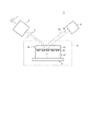
図1を参照して、本発明の一実施形態による膜厚測定装置1は、光源2と、干渉計3と、照射室4と、検出器5と、制御部(不図示)と、を備える。光源2は、ピーク波長が2.5〜25μmの範囲内に位置する赤外光を出射する。なお、光源2としては、例えば高輝度セラミックス光源を用いることができる。干渉計3は、光源2から出射した赤外光の光路上に配置され、光源2から出射した赤外光から干渉光L,L’を生成する。なお、干渉計3として、例えば公知のマイケルソン干渉計を用いることができる。照射室4には、干渉光L,L’の光路上に埋込み拡散層付きエピタキシャルシリコンウェーハWが位置するように、埋込み拡散層付きエピタキシャルシリコンウェーハWを載置するための測定ステージ6が配置される。検出器5は、埋込み拡散層付きエピタキシャルシリコンウェーハWからの第1,第2の反射光R1,R2の光路上に配置され、これらの反射光を検出する。検出器5として、例えばDTGSなどの焦電検知器を用いることができる。制御部は、検出器5の出力に基づき、シリコンエピタキシャル層18の膜厚を算出する。なお、制御部は、コンピュータ内部の中央演算処理装置(CPU)等によって実現することができる。
(Film thickness measuring device)
Referring to FIG. 1, a film thickness measuring device 1 according to one embodiment of the present invention includes a
測定ステージ6は、赤外光のスペクトルのピーク波長における反射率が15%以下である材質からなる。より好ましくは、赤外光のスペクトルのピーク波長における反射率が10%以下である材質からなる。具体的には、測定ステージ6は、石英、フッ素樹脂、及びセラミックスのうちから選択される1つ以上の材質からなることが好ましい。この技術的意義については後述する。また、測定ステージ6は、上述した反射率を有する単一の材質からなるものでもよい。あるいは、測定ステージ6は、反射率が15%以下の第1の材質と、当該第1の材質の上に積層され、かつ反射率が10%以下の第2の材質と、からなるものであってもよい。また、測定ステージ6がウェーハ裏面全体と接触しないものである場合には、測定ステージ6のうち、ウェーハ裏面が接触する部分と、ウェーハ裏面が接触しない部分との反射率の差を小さくすることがより好ましい。具体的には、反射率の差を1%以下とすることがより好ましい。
The
測定ステージ6の機械的強度を高める観点から、セラミックスを選択することがより好ましい。また、測定ステージ6の清浄度を高める観点から、フッ素樹脂を選択することがより好ましい。機械的強度と清浄度を高める観点から、測定ステージ6の母材をセラミックスとし、当該母材の表面をフッ素樹脂で被覆することがさらに好ましい。セラミックスとしては、炭化珪素やブラックアルミナが挙げられる。フッ素樹脂としては、ポリテトラフルオロエチレン(PTFE)、パーフルオロアルコキシアルカン(PFA)、四フッ化エチレン・六フッ化プロピレン共重合体(FEP)、エチレン・四フッ化エチレン共重合体 (ETFE)、ポリビニリデンフルオライド(PVDF)、ポリクロロトリフルオロエチレン(PCTFE)、及びエチレン・クロロトリフルオロエチレン共重合体(ECTFE)のうちから選択される1つ以上の樹脂が挙げられる。
From the viewpoint of increasing the mechanical strength of the measuring
なお、測定ステージ6は、一般的なウェーハ搬送用エンドエフェクタにおけるウェーハ保持部であってもよい。ただし、ウェーハ保持部は、上述した赤外光のスペクトルのピーク波長における反射率が15%以下である材質からなることが重要である。
The
(膜厚測定方法)
以下では、上述した膜厚測定装置1を用いて行うことが可能な、埋込み拡散層付きエピタキシャルシリコンウェーハWにおけるシリコンエピタキシャル層18の膜厚測定方法の一例を説明する。
(Film thickness measurement method)
Hereinafter, an example of a method of measuring the film thickness of the
まず、本実施形態による膜厚測定方法に供することが可能な埋込み拡散層付きエピタキシャルシリコンウェーハWを説明する。図1を参照して、埋込み拡散層付きエピタキシャルシリコンウェーハWは、シリコン基板10と、シリコン基板10の表層に形成された埋込み拡散層16と、埋込み拡散層16上に形成されたシリコンエピタキシャル層18と、を有する。
First, the epitaxial silicon wafer W with a buried diffusion layer that can be used in the film thickness measurement method according to the present embodiment will be described. Referring to FIG. 1, an epitaxial silicon wafer W with a buried diffusion layer includes a
図3を参照して、シリコン基板のドーパント濃度が低い埋込み拡散層付きエピタキシャルシリコンウェーハWでは、干渉光L’は、シリコンエピタキシャル層18とシリコン基板10を透過して、埋込み拡散層付きエピタキシャルシリコンウェーハWと測定ステージ7との界面に到達する。すると、この干渉光が反射光となりシリコンエピタキシャル層18の膜厚測定に悪影響を及ぼす。ところが、詳細は後述するが、このようなドーパント濃度の埋込み拡散層付きエピタキシャルシリコンウェーハWを本実施形態による膜厚測定装置または膜厚測定方法に供すると、この反射光の強度を抑制することができる。その結果、シリコンエピタキシャル層18の膜厚を高精度に測定することができる。シリコン基板10のドーパント濃度が高い場合、干渉光L’は、シリコン基板10とシリコンエピタキシャル層18との界面や、埋込み拡散層16とシリコンエピタキシャル層18との界面で完全に反射するので、図3につき説明した上記問題は生じない。デバイス工程における埋込み拡散層による絶縁性等を確保する観点から、シリコン基板10のドーパント濃度は、p型の場合には1.3×10¹⁵〜2.8×10¹⁷atoms/cm3とすることが好ましい。なお、デバイス構造の理由から、シリコンエピタキシャル層18のドーパントの種類はn型が広く使われている。ただし、シリコン基板とシリコンエピタキシャル層の導電型は、この組み合わせに限定されず、n/n+、n/p+、p/p+、n/p/p+、n/n+/p+構造などが挙げられる。
With reference to FIG. 3, in the epitaxial silicon wafer W with a buried diffusion layer in which the dopant concentration of the silicon substrate is low, the interference light L′ passes through the
埋込み拡散層16における不純物の濃度は、埋め込み拡散層における干渉光の反射を用いてエピタキシャル層の厚さを測定する必要があるので、不純物がP(リン)である場合、1.0×10¹⁸atoms/cm2以上であることが好ましく、不純物がB(ボロン)である場合、3.0×1018atoms/cm2以上であることが好ましく、不純物がAsまたはSbである場合も、1.0×1018atoms/cm2以上であることが好ましい。なお、埋込み拡散層16が形成される領域は、デバイス形成工程にて作製する集積回路の回路パターンに応じて適宜設定することができる。例えば、埋込み拡散層付きエピタキシャルシリコンウェーハWを平面視した場合において、シリコン基板10の表面全体に対する埋込み拡散層16の面積の割合は20〜99%とすることができる。より好ましくは20〜60%、さらに好ましくは20〜40%である。20%以上であれば、エピタキシャル層の厚さを安定的に測定することができ、60%以下であれば、ノイズの発生を抑制することができるからである。また、埋込み拡散層16の厚さは1.0〜20.0μm、好ましくは2.0〜5.0μmとすることができる。
As for the concentration of impurities in the buried
本実施形態では、以下に説明する第1〜第3工程を経ることによって、埋込み拡散層付きエピタキシャルシリコンウェーハWにおけるシリコンエピタキシャル層18の膜厚を測定することができる。
In the present embodiment, the film thickness of the
[第1工程:干渉光の生成]
図1を参照して、第1工程では、干渉計3を用いて、光源2から出射した赤外光から干渉光L,L’を生成する。ここで、赤外光のピーク波長は、2.5〜25μmの範囲から選択することができる。なお、干渉光L,L’を生成する方法は、特に限定されず、例えば公知のマイケルソン干渉計を用いて行うことができる。
[First step: generation of interference light]
Referring to FIG. 1, in a first step, interferometer 3 is used to generate interference lights L and L′ from infrared light emitted from
[第2工程:干渉光の照射]
図1を参照して、第2工程では、照射室4内の測定ステージ6に載置された埋込み拡散層付きエピタキシャルシリコンウェーハWに、干渉光L,L’を照射する。照射した干渉光Lは、第1の反射光R1と第2の反射光R2となって、埋込み拡散層付きエピタキシャルシリコンウェーハWから出射する。ここで、第1の反射光R1は、干渉光Lがシリコンエピタキシャル層18の表面で反射することによって生じる反射光である。第2の反射光R2は、干渉光Lがシリコンエピタキシャル層18を透過し、シリコンエピタキシャル層18と埋込み拡散層16との界面で反射することによって生じる反射光である。
[Second step: irradiation of interference light]
With reference to FIG. 1, in the second step, the interference light L, L′ is irradiated to the epitaxial silicon wafer W with the embedded diffusion layer mounted on the
[第3工程:膜厚の算出]
図1を参照して、第3工程では、第2工程で生じた第1の反射光R1と第2の反射光R2とを検出器5にて検出する。そして、制御部(不図示)が、検出器5から出力された第1の反射光R1および第2の反射光R2のインタフェログラムのピーク波長と、第1の反射光R1および第2の反射光R2の光路差を公知のFTIR法を用いて解析する。これにより、シリコンエピタキシャル層18の膜厚が算出される。
[Third step: calculation of film thickness]
Referring to FIG. 1, in the third step, the detector 5 detects the first reflected light R1 and the second reflected light R2 generated in the second step. Then, the control unit (not shown) causes the peak wavelengths of the interferograms of the first reflected light R1 and the second reflected light R2 output from the detector 5, and the first reflected light R1 and the second reflected light. The optical path difference of R2 is analyzed using a known FTIR method. As a result, the film thickness of the
以下では、図1及び図3(A),(B)を適宜参照して、本発明の技術的意義を説明する。図3(A)を参照して、第2工程では、第1の反射光R1と第2の反射光R2の他に、干渉光L’から生じた第3の反射光R3が存在する。すなわち、第3の反射光R3は、干渉光L’がシリコンエピタキシャル層18を透過した後に、シリコン基板10の表層のうち埋込み拡散層16が形成されていない領域を透過し、埋込み拡散層付きエピタキシャルシリコンウェーハWと測定ステージ7との界面で反射することによって生じる反射光である。ここで、図3(B)も参照して、第3の反射光R3の強度が強いと、第3工程で解析するインタフェログラムにおいて、シリコンエピタキシャル層18の膜厚に相当するピークと同程度の大きさのノイズが発生してしまう。このノイズは、通常、較正により取り除く試みがなされているが、較正を行う際の計測位置(例えばセンター1点のみ)や測定ステージの構造(例えば、測定ステージがウェーハ裏面全体と接触しない構造)に起因して、較正が不十分になる。そのため、制御部が、ノイズに含まれる複数のピークをシリコンエピタキシャル層18の膜厚に相当するピークとして誤って認識してしまい、シリコンエピタキシャル層18の膜厚が誤って算出される場合がある。これに対して、本実施形態では、測定ステージ7が、赤外光のスペクトルのピーク波長における反射率が15%以下である材質からなるので、干渉光L’から生じる第3の反射光の強度を低減することができる。これにより、第1の反射光R1および第2の反射光R2のインタフェログラムにおけるノイズを低減することができ、その結果、シリコンエピタキシャル層18の膜厚を高精度に測定することができる。なお、測定ステージの表面のみを、反射率が15%以下である第1の材質で構成し、測定ステージの表面以外の部分を、反射率が15%を超える第2の材質で構成したとしても、測定ステージに入射した干渉光は、第1の材質と第2の材質との界面で反射するので、ノイズが発生してしまう。そのため、測定ステージの表面のみを、反射率が15%以下である材質で構成しても本発明の効果を得ることはできない。
Hereinafter, the technical significance of the present invention will be described with reference to FIGS. 1 and 3A and 3B as appropriate. Referring to FIG. 3A, in the second step, in addition to the first reflected light R1 and the second reflected light R2, there is the third reflected light R3 generated from the interference light L'. That is, the third reflected light R3 is transmitted through the
(埋込み拡散層付きエピタキシャルシリコンウェーハの製造方法)
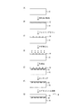
以下、図2を参照して、上述した膜厚測定装置または膜厚測定方法を用いて行うことが可能な、埋込み拡散層付きエピタキシャルシリコンウェーハWの製造方法の一例を説明する。
(Method of manufacturing epitaxial silicon wafer with embedded diffusion layer)
Hereinafter, with reference to FIG. 2, an example of a method of manufacturing an epitaxial silicon wafer W with a buried diffusion layer, which can be performed using the above-described film thickness measuring device or film thickness measuring method, will be described.
[第1工程:パターン付き酸化膜の形成]
第1工程では、シリコン基板10の表面に酸化膜12を形成した後に(図2(A),(B))、フォトリソグラフィ法により、酸化膜12をパターン付き酸化膜14とする(図2(B),(C))。酸化膜12の形成方法は、特に限定されず、公知の熱酸化法や化学気相成長(CVD:chemical vapor deposition)法などを好適に用いればよい。フォトリソグラフィ法は、特に限定されず、公知の方法を好適に用いればよい。なお、パターン付き酸化膜14のパターンは、デバイス形成工程にて埋込み拡散層16に形成する集積回路の回路パターンに応じて適宜設定することができる。また、シリコン基板10としては、チョクラルスキ法(CZ法)や浮遊帯域溶融法(FZ法)により育成した単結晶シリコンインゴットから得た単結晶シリコン基板に対して、B(ボロン)などのドーパントを1.3×10¹⁵〜2.8×10¹⁷atoms/cm3の濃度で添加したものを用いることができる。
[First step: formation of patterned oxide film]
In the first step, after forming the
[第2工程:埋込み拡散層の形成]
第2工程では、シリコン基板10に対して、パターン付き酸化膜14側から不純物を注入した後に(図2(C),(D))、熱処理を施すことによって、シリコン基板10の表層に埋込み拡散層16を形成する(図2(D),(E))。不純物をPとする場合は、1.0×10¹²atoms/cm2以上のドーズ量で注入することが好ましく、不純物をBとする場合は、1.0×1013atoms/cm2以上のドーズ量で注入することが好ましく、不純物をAsまたはSbとする場合は、1.0×1014atoms/cm2以上のドーズ量で注入することが好ましい。これらの理由は既述の説明を援用する。また、シリコン基板10の表面全体に対する埋込み拡散層16の面積の割合を20〜99%として、埋込み拡散層16の厚さを1.0〜20.0μm(好ましくは2.0〜5.0μm)とする観点から、熱処理は、酸化雰囲気下、1000〜1250℃、1〜30時間とすることが好ましい。
[Second step: formation of buried diffusion layer]
In the second step, impurities are implanted into the
[第3工程:パターン付き酸化膜の除去]
第3工程では、パターン付き酸化膜14を除去する(図2(E),(F))。なお、パターン付き酸化膜14を除去する方法は、特に限定されず、例えばフッ酸などのエッチング液を好適に用いることができる。
[Third step: removal of patterned oxide film]
In the third step, the patterned
[第4工程:シリコンエピタキシャル層の形成]
第4工程では、埋込み拡散層16上にシリコンエピタキシャル層18を形成する(図2(F),(G))。例えば、CVD法により、キャリアガスを水素とし、原料ガスをジクロロシラン、トリクロロシラン等とし、基板温度を1000℃以上1150℃以下として、シリコンエピタキシャル層18を成長させることができる。なお、シリコンエピタキシャル層18の厚さは、0.5μm以上15μm以下の範囲から適宜選択すればよい。
[Fourth step: formation of silicon epitaxial layer]
In the fourth step, the
[第5工程:膜厚測定]
図1も参照して、第5工程では、上述した膜厚測定装置または膜厚測定方法を用いてシリコンエピタキシャル層18の膜厚を測定する。これにより、シリコンエピタキシャル層18の膜厚を高精度に測定することができる。なお、詳細については、既述の説明を援用する。
[Fifth step: film thickness measurement]
Referring also to FIG. 1, in the fifth step, the film thickness of the
以上、本実施形態を例にして、本発明の埋込み拡散層付きエピタキシャルシリコンウェーハにおけるシリコンエピタキシャル層の膜厚測定装置および膜厚測定方法、ならびに当該膜厚測定装置または当該膜厚測定方法を用いた埋込み拡散層付きエピタキシャルシリコンウェーハの製造方法を説明した。ただし、本発明は、上記実施形態に限定されず、特許請求の範囲において適宜変更を加えることができる。 As described above, by using this embodiment as an example, the film thickness measuring device and the film thickness measuring method of the silicon epitaxial layer in the epitaxial silicon wafer with the buried diffusion layer of the present invention, and the film thickness measuring device or the film thickness measuring method were used. The method of manufacturing an epitaxial silicon wafer with a buried diffusion layer has been described. However, the present invention is not limited to the above-mentioned embodiment, and appropriate modifications can be made within the scope of the claims.
(発明例)
本発明の効果を確かめるために、発明例として、以下に説明する埋込み拡散層付きエピタキシャルシリコンウェーハおよび膜厚測定装置を作製し、シリコンエピタキシャル層の膜厚を測定した。
(Invention example)
In order to confirm the effect of the present invention, as an example of the invention, an epitaxial silicon wafer with a buried diffusion layer and a film thickness measuring device described below were produced, and the film thickness of the silicon epitaxial layer was measured.
[埋込み拡散層付きエピタキシャルシリコンウェーハの作製]
CZ法により得たシリコン基板(ドーパント:ボロン、ドーパント濃度:1.3×10¹⁵atoms/cm3)の表面に、酸化膜を熱酸化法により形成した(図2(A),(B))。その後、フォトリソグラフィ法により、酸化膜をパターン付き酸化膜とした(図2(B),(C))。次に、シリコン基板に対して、パターン付き酸化膜側からSbを5×1014atoms/cm2のドーズ量で注入した(図2(C),(D))。その後、熱処理を施すことによって、埋込み拡散層を形成した(図2(D),(E))。なお、シリコン基板を平面視した場合において、シリコン基板の表面全体に対する埋込み拡散層の面積の割合は30%であり、埋込み拡散層の厚さは2.0μmであった。次に、フッ酸を用いて、パターン付き酸化膜を除去した(図2(E),(F))。次に、CVD法を用いて、キャリアガスを水素とし、ソースガスをジクロロシランとし、基板温度を1080℃として、埋込み拡散上にシリコンエピタキシャル層(ドーパント:リン、ドーパント濃度:5×1015atoms/cm3)を形成した(図2(F),(G))。このようにして埋込み拡散層付きエピタキシャルシリコンウェーハを得た。
[Fabrication of epitaxial silicon wafer with embedded diffusion layer]
An oxide film was formed by a thermal oxidation method on the surface of a silicon substrate (dopant: boron, dopant concentration: 1.3×10 15 atoms/cm 3 ) obtained by the CZ method (FIGS. 2A and 2B). .. Then, the oxide film was formed into a patterned oxide film by the photolithography method (FIGS. 2B and 2C). Next, Sb was implanted into the silicon substrate from the patterned oxide film side at a dose of 5×10 14 atoms/cm 2 (FIGS. 2C and 2D). Then, heat treatment was performed to form a buried diffusion layer (FIGS. 2D and 2E). In the plan view of the silicon substrate, the area ratio of the embedded diffusion layer to the entire surface of the silicon substrate was 30%, and the thickness of the embedded diffusion layer was 2.0 μm. Next, the patterned oxide film was removed using hydrofluoric acid (FIGS. 2E and 2F). Then, using a CVD method, hydrogen is used as a carrier gas, dichlorosilane is used as a source gas, the substrate temperature is 1080° C., and a silicon epitaxial layer (dopant: phosphorus; dopant concentration: 5×10 15 atoms/ cm 3 ) was formed (FIGS. 2F and 2G). Thus, an epitaxial silicon wafer with a buried diffusion layer was obtained.
[膜厚測定装置の作製]
図1に示す、光源と、干渉計と、測定ステージ(ウェーハ搬送用エンドエフェクタにおけるウェーハ保持部)が配置された照射室と、検出器と、制御部(不図示)と、を備える膜厚測定装置を作製した。光源として、出射する赤外光のスペクトルのピーク波長が12.5μmとなるもの用いた。測定ステージとして、アルミナセラミックスを母材として、当該母材の表面に導電性黒色テフロンを被覆したものを用いた。赤外光のスペクトルのピーク波長(12.5μm)における、アルミナセラミックスの反射率は8%であり、導電性黒色テフロンの反射率は7%であった。
[Production of film thickness measuring device]
A film thickness measurement including a light source, an interferometer, an irradiation chamber in which a measurement stage (a wafer holding unit in a wafer transfer end effector) is arranged, a detector, and a control unit (not shown) shown in FIG. The device was made. A light source having a peak wavelength of 12.5 μm in the spectrum of emitted infrared light was used. As the measurement stage, a base material made of alumina ceramics and the surface of the base material coated with conductive black Teflon was used. At the peak wavelength (12.5 μm) of the spectrum of infrared light, the reflectance of the alumina ceramics was 8% and the reflectance of the conductive black Teflon was 7%.
[膜厚の測定]
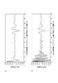
この膜厚測定装置を用いて、上述した膜厚測定方法により、シリコンエピタキシャル層の膜厚を測定した。検出器によって検出したインタフェログラムを図4(A)に示す。
[Measurement of film thickness]
Using this film thickness measuring device, the film thickness of the silicon epitaxial layer was measured by the film thickness measuring method described above. The interferogram detected by the detector is shown in FIG.
(比較例)
測定ステージとして、ステンレス鋼を母材して、当該母材の表面にテフロン(登録商標)を被覆したものを用いた以外は、発明例と同様の方法により、シリコンエピタキシャル層の膜厚を測定した。なお、赤外光のスペクトルのピーク波長(12.5μm)における、ステンレス鋼の反射率は70%であり、テフロン(登録商標)の反射率は7%であった。検出器によって検出したインタフェログラムを図4(B)に示す。
(Comparative example)
The film thickness of the silicon epitaxial layer was measured by the same method as in the inventive example except that a stainless steel base material was used as the measurement stage and the surface of the base material was coated with Teflon (registered trademark). .. The reflectance of stainless steel was 70% and the reflectance of Teflon (registered trademark) was 7% at the peak wavelength (12.5 μm) of the spectrum of infrared light. The interferogram detected by the detector is shown in FIG.
(評価結果および評価結果の説明)
図4(B)に示す比較例では、シリコンエピタキシャル層の膜厚(13μm)に相当するピークと同程度の大きさのピークを複数有するノイズが発生した。これに対して、図4(A)に示す発明例では、図4(B)に示すようなノイズを低減することができており、シリコンエピタキシャル層の膜厚が13μmであることが正確にわかった。これは、発明例では、赤外光のスペクトルのピーク波長における、測定ステージの材質(すなわち、アルミナセラミックスとテフロン(登録商標))の反射率を15%以下にしたことによって、検出器に入射する第3の反射光の強度を弱めることができたことに起因する。
(Evaluation results and explanation of evaluation results)
In the comparative example shown in FIG. 4B, noise having a plurality of peaks having the same magnitude as the peak corresponding to the film thickness (13 μm) of the silicon epitaxial layer was generated. On the other hand, in the example of the invention shown in FIG. 4(A), the noise as shown in FIG. 4(B) can be reduced, and it is accurately understood that the film thickness of the silicon epitaxial layer is 13 μm. It was This is because in the invention example, the reflectance of the material of the measuring stage (that is, alumina ceramics and Teflon (registered trademark)) is set to 15% or less at the peak wavelength of the spectrum of infrared light, so that it enters the detector. This is because the intensity of the third reflected light could be weakened.
本発明によれば、シリコン基板のドーパント濃度が低い埋込み拡散層付きエピタキシャルシリコンウェーハであっても、シリコンエピタキシャル層の膜厚を高精度に測定することができる。 According to the present invention, the film thickness of a silicon epitaxial layer can be measured with high accuracy even in an epitaxial silicon wafer with a buried diffusion layer in which the dopant concentration of the silicon substrate is low.
1 膜厚測定装置
2 光源
3 干渉計
4 照射室
5 検出器
6,7 測定ステージ
10 シリコン基板
12 酸化膜
14 パターン付き酸化膜
16 埋込み拡散層
18 シリコンエピタキシャル層
W 埋込み拡散層付きエピタキシャルシリコンウェーハ
L,L’ 干渉光
R1 第1の反射光
R2 第2の反射光
1 Film
Claims (7)
赤外光を出射する光源と、
前記赤外光の光路上に配置され、かつ、前記赤外光から、前記埋込み拡散層付きエピタキシャルシリコンウェーハに照射するための干渉光を生成する干渉計と、
前記干渉光の光路上に前記埋込み拡散層付きエピタキシャルシリコンウェーハが位置するように、前記埋込み拡散層付きエピタキシャルシリコンウェーハを載置するための測定ステージと、
前記干渉光が前記シリコンエピタキシャル層の表面で反射することによって生じる第1の反射光と、前記干渉光が前記シリコンエピタキシャル層を透過して、前記シリコンエピタキシャル層と前記埋込み拡散層との界面で反射することによって生じる第2の反射光と、の光路上に配置され、かつ、前記第1の反射光と前記第2の反射光を検出する検出器と、
前記検出器の出力に基づき、前記シリコンエピタキシャル層の膜厚を算出する制御部と、
を備え、
前記測定ステージは、前記赤外光のスペクトルのピーク波長における反射率が15%以下である材質からなることを特徴とする膜厚測定装置。 A silicon substrate, a buried diffusion layer formed on the surface layer of the silicon substrate, and a silicon epitaxial layer formed on the buried diffusion layer, a film thickness of the silicon epitaxial layer in the epitaxial silicon wafer with a buried diffusion layer A film thickness measuring device for measuring,
A light source that emits infrared light,
Arranged on the optical path of the infrared light, and, from the infrared light, an interferometer for generating interference light for irradiating the epitaxial silicon wafer with the buried diffusion layer,
The measurement stage for mounting the epitaxial silicon wafer with the buried diffusion layer so that the buried diffusion layer with the epitaxial silicon wafer is located on the optical path of the interference light,
First reflected light generated by the interference light being reflected on the surface of the silicon epitaxial layer, and the interference light being transmitted through the silicon epitaxial layer and reflected at the interface between the silicon epitaxial layer and the buried diffusion layer. A detector that is disposed on the optical path of the second reflected light generated by the above, and that detects the first reflected light and the second reflected light;
A control unit for calculating the film thickness of the silicon epitaxial layer based on the output of the detector;
Equipped with
The film thickness measuring device, wherein the measuring stage is made of a material having a reflectance of 15% or less at a peak wavelength of the spectrum of the infrared light.
赤外光から干渉光を生成し、
測定ステージに載置された前記埋込み拡散層付きエピタキシャルシリコンウェーハに、前記干渉光を照射し、
前記干渉光が前記シリコンエピタキシャル層の表面で反射することによって生じる第1の反射光と、前記干渉光が前記シリコンエピタキシャル層を透過して、前記シリコンエピタキシャル層と前記埋込み拡散層との界面で反射することによって生じる第2の反射光とを検出し、
前記シリコンエピタキシャル層の膜厚を算出し、
前記測定ステージは、前記赤外光のスペクトルのピーク波長における反射率が15%以下である材質からなることを特徴とする膜厚測定方法。 A silicon substrate, a buried diffusion layer formed on the surface layer of the silicon substrate, and a silicon epitaxial layer formed on the buried diffusion layer, a film thickness of the silicon epitaxial layer in the epitaxial silicon wafer with a buried diffusion layer A film thickness measuring method for measuring,
Generates interference light from infrared light,
Irradiating the interference light to the epitaxial silicon wafer with the embedded diffusion layer placed on the measurement stage,
First reflected light generated by the interference light being reflected on the surface of the silicon epitaxial layer, and the interference light being transmitted through the silicon epitaxial layer and reflected at the interface between the silicon epitaxial layer and the buried diffusion layer. Detecting the second reflected light generated by
Calculate the film thickness of the silicon epitaxial layer,
The film thickness measuring method, wherein the measuring stage is made of a material having a reflectance of 15% or less at a peak wavelength of the spectrum of infrared light.
その後、前記シリコン基板に対して、前記パターン付き酸化膜側から不純物を注入した後に、熱処理を施すことによって、前記シリコン基板の表層に埋込み拡散層を形成し、
その後、前記パターン付き酸化膜を除去し、
その後、前記埋込み拡散上に、シリコンエピタキシャル層を形成し、
その後、請求項1〜3のいずれか一項に記載の装置または請求項4〜6のいずれか一項に記載の方法を用いて前記シリコンエピタキシャル層の膜厚を測定することを特徴とする埋込み拡散層付きエピタキシャルシリコンウェーハの製造方法。 After forming an oxide film on the surface of the silicon substrate, the oxide film as a patterned oxide film by photolithography,
After that, an impurity is injected into the silicon substrate from the patterned oxide film side, and then a heat treatment is performed to form a buried diffusion layer in the surface layer of the silicon substrate,
Then, the patterned oxide film is removed,
Then, a silicon epitaxial layer is formed on the buried diffusion,
Thereafter, the film thickness of the silicon epitaxial layer is measured by using the apparatus according to any one of claims 1 to 3 or the method according to any one of claims 4 to 6. Manufacturing method of epitaxial silicon wafer with diffusion layer.
Priority Applications (1)
| Application Number | Priority Date | Filing Date | Title |
|---|---|---|---|
| JP2018240172A JP7028154B2 (en) | 2018-12-21 | 2018-12-21 | A film thickness measuring device and a film thickness measuring method for a silicon epitaxial layer in an epitaxial silicon wafer with an embedded diffusion layer, and a method for manufacturing an epitaxial silicon wafer with an embedded diffusion layer using the film thickness measuring device or the film thickness measuring method. |
Applications Claiming Priority (1)
| Application Number | Priority Date | Filing Date | Title |
|---|---|---|---|
| JP2018240172A JP7028154B2 (en) | 2018-12-21 | 2018-12-21 | A film thickness measuring device and a film thickness measuring method for a silicon epitaxial layer in an epitaxial silicon wafer with an embedded diffusion layer, and a method for manufacturing an epitaxial silicon wafer with an embedded diffusion layer using the film thickness measuring device or the film thickness measuring method. |
Publications (2)
| Publication Number | Publication Date |
|---|---|
| JP2020101460A true JP2020101460A (en) | 2020-07-02 |
| JP7028154B2 JP7028154B2 (en) | 2022-03-02 |
Family
ID=71139479
Family Applications (1)
| Application Number | Title | Priority Date | Filing Date |
|---|---|---|---|
| JP2018240172A Active JP7028154B2 (en) | 2018-12-21 | 2018-12-21 | A film thickness measuring device and a film thickness measuring method for a silicon epitaxial layer in an epitaxial silicon wafer with an embedded diffusion layer, and a method for manufacturing an epitaxial silicon wafer with an embedded diffusion layer using the film thickness measuring device or the film thickness measuring method. |
Country Status (1)
| Country | Link |
|---|---|
| JP (1) | JP7028154B2 (en) |
Cited By (3)
| Publication number | Priority date | Publication date | Assignee | Title |
|---|---|---|---|---|
| CN113884015A (en) * | 2021-09-23 | 2022-01-04 | 苏州微创关节医疗科技有限公司 | Metal oxide ceramic layer thickness measuring system and thickness measuring method thereof |
| CN116313808A (en) * | 2023-03-14 | 2023-06-23 | 上海华力集成电路制造有限公司 | Method for Monitoring Indexes of Epitaxially Grown Embedded SiGe |
| CN121185195A (en) * | 2025-11-25 | 2025-12-23 | 山东管理学院 | Methods, systems, media and equipment for infrared measurement of silicon carbide epitaxial layer thickness |
Citations (3)
| Publication number | Priority date | Publication date | Assignee | Title |
|---|---|---|---|---|
| JPS6352004A (en) * | 1986-08-22 | 1988-03-05 | Hitachi Micro Comput Eng Ltd | measuring device |
| JPH02152250A (en) * | 1988-12-02 | 1990-06-12 | Nec Corp | Evaluation of epitaxial growth layer |
| JP2013148448A (en) * | 2012-01-19 | 2013-08-01 | Toppan Printing Co Ltd | Method for inspecting optical film |
-
2018
- 2018-12-21 JP JP2018240172A patent/JP7028154B2/en active Active
Patent Citations (3)
| Publication number | Priority date | Publication date | Assignee | Title |
|---|---|---|---|---|
| JPS6352004A (en) * | 1986-08-22 | 1988-03-05 | Hitachi Micro Comput Eng Ltd | measuring device |
| JPH02152250A (en) * | 1988-12-02 | 1990-06-12 | Nec Corp | Evaluation of epitaxial growth layer |
| JP2013148448A (en) * | 2012-01-19 | 2013-08-01 | Toppan Printing Co Ltd | Method for inspecting optical film |
Cited By (3)
| Publication number | Priority date | Publication date | Assignee | Title |
|---|---|---|---|---|
| CN113884015A (en) * | 2021-09-23 | 2022-01-04 | 苏州微创关节医疗科技有限公司 | Metal oxide ceramic layer thickness measuring system and thickness measuring method thereof |
| CN116313808A (en) * | 2023-03-14 | 2023-06-23 | 上海华力集成电路制造有限公司 | Method for Monitoring Indexes of Epitaxially Grown Embedded SiGe |
| CN121185195A (en) * | 2025-11-25 | 2025-12-23 | 山东管理学院 | Methods, systems, media and equipment for infrared measurement of silicon carbide epitaxial layer thickness |
Also Published As
| Publication number | Publication date |
|---|---|
| JP7028154B2 (en) | 2022-03-02 |
Similar Documents
| Publication | Publication Date | Title |
|---|---|---|
| US6200388B1 (en) | Substrate support for a thermal processing chamber | |
| WO2017141486A1 (en) | Silicon carbide epitaxial substrate and method for manufacturing silicon carbide semiconductor device | |
| JP7028154B2 (en) | A film thickness measuring device and a film thickness measuring method for a silicon epitaxial layer in an epitaxial silicon wafer with an embedded diffusion layer, and a method for manufacturing an epitaxial silicon wafer with an embedded diffusion layer using the film thickness measuring device or the film thickness measuring method. | |
| CN115161623A (en) | Dual pyrometer system for substrate temperature control during film deposition | |
| TW200842332A (en) | Substrate temperature measurement by infrared transmission | |
| CN110998787B (en) | Epitaxially coated semiconductor wafer composed of single crystal silicon and method of manufacturing same | |
| JP2004311580A (en) | Semiconductor evaluation apparatus and semiconductor evaluation method | |
| JP6180924B2 (en) | Heat flux measurement method, substrate processing system, and heat flux measurement member | |
| JP2015516685A5 (en) | ||
| TW202117272A (en) | Thickness measuring method of semiconductor wafer and thickness measuring system of semiconductor wafer | |
| TWI343474B (en) | Methods and apparatus for determining the temperature of a substrate | |
| KR101555547B1 (en) | Method for manufacturing sic semiconductor device | |
| JP4166400B2 (en) | Radiation temperature measurement method | |
| JP6462892B2 (en) | Manufacturing method of solar cell | |
| TW202115362A (en) | Thickness measuring method of semiconductor wafer and thickness measuring system of semiconductor wafer | |
| WO2024058044A1 (en) | Silicon carbide epitaxial substrate, method for manufacturing epitaxial substrate, and method for manufacturing silicon carbide semiconductor device | |
| Lowney et al. | Investigation of strain induced effects in silicon wafers due to proximity rapid thermal processing using micro-Raman spectroscopy and synchrotron x-ray topography | |
| JPH0982768A (en) | Semiconductor wafer evaluation method | |
| Mäkelä et al. | Decreasing Defect‐State Density of Al2O3/GaxIn1− xAs Device Interfaces with InOx Structures | |
| JP7631457B1 (en) | Optical heating method and optical heating device for n-type SiC semiconductor | |
| JP3788606B2 (en) | Surface photovoltaic measurement method | |
| US9842958B2 (en) | Ultrananocrystalline diamond contacts for electronic devices | |
| CN110036463B (en) | Method for manufacturing semiconductor substrate | |
| Sampson et al. | Wavelength considerations for improved silicon wafer temperature measurement by ellipsometry | |
| US20240145274A1 (en) | Low temperature measurement of semiconductor substrates |
Legal Events
| Date | Code | Title | Description |
|---|---|---|---|
| A621 | Written request for application examination |
Free format text: JAPANESE INTERMEDIATE CODE: A621 Effective date: 20201221 |
|
| A977 | Report on retrieval |
Free format text: JAPANESE INTERMEDIATE CODE: A971007 Effective date: 20211102 |
|
| A131 | Notification of reasons for refusal |
Free format text: JAPANESE INTERMEDIATE CODE: A131 Effective date: 20211116 |
|
| A521 | Request for written amendment filed |
Free format text: JAPANESE INTERMEDIATE CODE: A523 Effective date: 20211227 |
|
| TRDD | Decision of grant or rejection written | ||
| A01 | Written decision to grant a patent or to grant a registration (utility model) |
Free format text: JAPANESE INTERMEDIATE CODE: A01 Effective date: 20220118 |
|
| A61 | First payment of annual fees (during grant procedure) |
Free format text: JAPANESE INTERMEDIATE CODE: A61 Effective date: 20220131 |
|
| R150 | Certificate of patent or registration of utility model |
Ref document number: 7028154 Country of ref document: JP Free format text: JAPANESE INTERMEDIATE CODE: R150 |
|
| R250 | Receipt of annual fees |
Free format text: JAPANESE INTERMEDIATE CODE: R250 |
|
| R250 | Receipt of annual fees |
Free format text: JAPANESE INTERMEDIATE CODE: R250 |