JP2020165902A - 検査装置 - Google Patents
検査装置 Download PDFInfo
- Publication number
- JP2020165902A JP2020165902A JP2019068623A JP2019068623A JP2020165902A JP 2020165902 A JP2020165902 A JP 2020165902A JP 2019068623 A JP2019068623 A JP 2019068623A JP 2019068623 A JP2019068623 A JP 2019068623A JP 2020165902 A JP2020165902 A JP 2020165902A
- Authority
- JP
- Japan
- Prior art keywords
- index table
- test
- mount
- semiconductor device
- inspection
- Prior art date
- Legal status (The legal status is an assumption and is not a legal conclusion. Google has not performed a legal analysis and makes no representation as to the accuracy of the status listed.)
- Pending
Links
Images






Classifications
-
- G—PHYSICS
- G01—MEASURING; TESTING
- G01R—MEASURING ELECTRIC VARIABLES; MEASURING MAGNETIC VARIABLES
- G01R31/00—Arrangements for testing electric properties; Arrangements for locating electric faults; Arrangements for electrical testing characterised by what is being tested not provided for elsewhere
- G01R31/26—Testing of individual semiconductor devices
- G01R31/2601—Apparatus or methods therefor
-
- G—PHYSICS
- G01—MEASURING; TESTING
- G01R—MEASURING ELECTRIC VARIABLES; MEASURING MAGNETIC VARIABLES
- G01R31/00—Arrangements for testing electric properties; Arrangements for locating electric faults; Arrangements for electrical testing characterised by what is being tested not provided for elsewhere
- G01R31/28—Testing of electronic circuits, e.g. by signal tracer
- G01R31/2851—Testing of integrated circuits [IC]
- G01R31/2855—Environmental, reliability or burn-in testing
- G01R31/286—External aspects, e.g. related to chambers, contacting devices or handlers
- G01R31/2865—Holding devices, e.g. chucks; Handlers or transport devices
- G01R31/2867—Handlers or transport devices, e.g. loaders, carriers, trays
-
- H—ELECTRICITY
- H10—SEMICONDUCTOR DEVICES; ELECTRIC SOLID-STATE DEVICES NOT OTHERWISE PROVIDED FOR
- H10P—GENERIC PROCESSES OR APPARATUS FOR THE MANUFACTURE OR TREATMENT OF DEVICES COVERED BY CLASS H10
- H10P72/00—Handling or holding of wafers, substrates or devices during manufacture or treatment thereof
- H10P72/30—Handling or holding of wafers, substrates or devices during manufacture or treatment thereof for conveying, e.g. between different workstations
- H10P72/33—Handling or holding of wafers, substrates or devices during manufacture or treatment thereof for conveying, e.g. between different workstations into and out of processing chamber
- H10P72/3304—Handling or holding of wafers, substrates or devices during manufacture or treatment thereof for conveying, e.g. between different workstations into and out of processing chamber characterised by movements or sequence of movements of transfer devices
-
- G—PHYSICS
- G01—MEASURING; TESTING
- G01R—MEASURING ELECTRIC VARIABLES; MEASURING MAGNETIC VARIABLES
- G01R31/00—Arrangements for testing electric properties; Arrangements for locating electric faults; Arrangements for electrical testing characterised by what is being tested not provided for elsewhere
- G01R31/28—Testing of electronic circuits, e.g. by signal tracer
- G01R31/2851—Testing of integrated circuits [IC]
- G01R31/2855—Environmental, reliability or burn-in testing
- G01R31/286—External aspects, e.g. related to chambers, contacting devices or handlers
- G01R31/2868—Complete testing stations; systems; procedures; software aspects
-
- G—PHYSICS
- G01—MEASURING; TESTING
- G01R—MEASURING ELECTRIC VARIABLES; MEASURING MAGNETIC VARIABLES
- G01R31/00—Arrangements for testing electric properties; Arrangements for locating electric faults; Arrangements for electrical testing characterised by what is being tested not provided for elsewhere
- G01R31/28—Testing of electronic circuits, e.g. by signal tracer
- G01R31/2851—Testing of integrated circuits [IC]
- G01R31/2855—Environmental, reliability or burn-in testing
- G01R31/2872—Environmental, reliability or burn-in testing related to electrical or environmental aspects, e.g. temperature, humidity, vibration, nuclear radiation
- G01R31/2874—Environmental, reliability or burn-in testing related to electrical or environmental aspects, e.g. temperature, humidity, vibration, nuclear radiation related to temperature
- G01R31/2875—Environmental, reliability or burn-in testing related to electrical or environmental aspects, e.g. temperature, humidity, vibration, nuclear radiation related to temperature related to heating
-
- G—PHYSICS
- G01—MEASURING; TESTING
- G01R—MEASURING ELECTRIC VARIABLES; MEASURING MAGNETIC VARIABLES
- G01R31/00—Arrangements for testing electric properties; Arrangements for locating electric faults; Arrangements for electrical testing characterised by what is being tested not provided for elsewhere
- G01R31/28—Testing of electronic circuits, e.g. by signal tracer
- G01R31/2851—Testing of integrated circuits [IC]
- G01R31/2893—Handling, conveying or loading, e.g. belts, boats, vacuum fingers
-
- H—ELECTRICITY
- H10—SEMICONDUCTOR DEVICES; ELECTRIC SOLID-STATE DEVICES NOT OTHERWISE PROVIDED FOR
- H10P—GENERIC PROCESSES OR APPARATUS FOR THE MANUFACTURE OR TREATMENT OF DEVICES COVERED BY CLASS H10
- H10P72/00—Handling or holding of wafers, substrates or devices during manufacture or treatment thereof
-
- H—ELECTRICITY
- H10—SEMICONDUCTOR DEVICES; ELECTRIC SOLID-STATE DEVICES NOT OTHERWISE PROVIDED FOR
- H10P—GENERIC PROCESSES OR APPARATUS FOR THE MANUFACTURE OR TREATMENT OF DEVICES COVERED BY CLASS H10
- H10P72/00—Handling or holding of wafers, substrates or devices during manufacture or treatment thereof
- H10P72/04—Apparatus for manufacture or treatment
- H10P72/0451—Apparatus for manufacturing or treating in a plurality of work-stations
- H10P72/0468—Apparatus for manufacturing or treating in a plurality of work-stations comprising a chamber adapted to a particular process
-
- H—ELECTRICITY
- H10—SEMICONDUCTOR DEVICES; ELECTRIC SOLID-STATE DEVICES NOT OTHERWISE PROVIDED FOR
- H10P—GENERIC PROCESSES OR APPARATUS FOR THE MANUFACTURE OR TREATMENT OF DEVICES COVERED BY CLASS H10
- H10P72/00—Handling or holding of wafers, substrates or devices during manufacture or treatment thereof
- H10P72/30—Handling or holding of wafers, substrates or devices during manufacture or treatment thereof for conveying, e.g. between different workstations
-
- H—ELECTRICITY
- H10—SEMICONDUCTOR DEVICES; ELECTRIC SOLID-STATE DEVICES NOT OTHERWISE PROVIDED FOR
- H10P—GENERIC PROCESSES OR APPARATUS FOR THE MANUFACTURE OR TREATMENT OF DEVICES COVERED BY CLASS H10
- H10P72/00—Handling or holding of wafers, substrates or devices during manufacture or treatment thereof
- H10P72/30—Handling or holding of wafers, substrates or devices during manufacture or treatment thereof for conveying, e.g. between different workstations
- H10P72/32—Handling or holding of wafers, substrates or devices during manufacture or treatment thereof for conveying, e.g. between different workstations between different workstations
- H10P72/3212—Handling or holding of wafers, substrates or devices during manufacture or treatment thereof for conveying, e.g. between different workstations between different workstations the substrates to be conveyed not being semiconductor wafers or large planar substrates, e.g. chips or lead frames
-
- H—ELECTRICITY
- H10—SEMICONDUCTOR DEVICES; ELECTRIC SOLID-STATE DEVICES NOT OTHERWISE PROVIDED FOR
- H10P—GENERIC PROCESSES OR APPARATUS FOR THE MANUFACTURE OR TREATMENT OF DEVICES COVERED BY CLASS H10
- H10P72/00—Handling or holding of wafers, substrates or devices during manufacture or treatment thereof
- H10P72/30—Handling or holding of wafers, substrates or devices during manufacture or treatment thereof for conveying, e.g. between different workstations
- H10P72/33—Handling or holding of wafers, substrates or devices during manufacture or treatment thereof for conveying, e.g. between different workstations into and out of processing chamber
- H10P72/3306—Horizontal transfer of a single workpiece
-
- G—PHYSICS
- G01—MEASURING; TESTING
- G01R—MEASURING ELECTRIC VARIABLES; MEASURING MAGNETIC VARIABLES
- G01R31/00—Arrangements for testing electric properties; Arrangements for locating electric faults; Arrangements for electrical testing characterised by what is being tested not provided for elsewhere
- G01R31/28—Testing of electronic circuits, e.g. by signal tracer
- G01R31/2851—Testing of integrated circuits [IC]
- G01R31/2855—Environmental, reliability or burn-in testing
- G01R31/286—External aspects, e.g. related to chambers, contacting devices or handlers
- G01R31/2868—Complete testing stations; systems; procedures; software aspects
- G01R31/287—Procedures; Software aspects
Landscapes
- Engineering & Computer Science (AREA)
- General Physics & Mathematics (AREA)
- Physics & Mathematics (AREA)
- Microelectronics & Electronic Packaging (AREA)
- General Engineering & Computer Science (AREA)
- Computer Hardware Design (AREA)
- Environmental & Geological Engineering (AREA)
- Health & Medical Sciences (AREA)
- Toxicology (AREA)
- Testing Of Individual Semiconductor Devices (AREA)
- Automatic Analysis And Handling Materials Therefor (AREA)
- Other Investigation Or Analysis Of Materials By Electrical Means (AREA)
- Spectrometry And Color Measurement (AREA)
Abstract
Description
本発明の一実施形態に係る検査装置1の概略構成について、図1を参照して説明する。図1は、検査装置1の概略構成を示す斜視図である。
検査装置1における半導体デバイスの搬送経路Pについて、図2を参照して説明する。図2は、搬送経路Pの構成を示す平面図である。
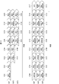
検査装置1を用いた検査方法S100の流れについて、図3を参照して説明する。図3は、検査方法S100の流れを示すフロー図である。なお、図3においては、各半導体デバイスDUTi(i=1,2,3,…)に対して順に適用される複数の工程を横に並べて示すと共に、複数の半導体デバイスDUT1,DUT2,DUT3,…に同時に適用される複数の工程を縦に並べて示している。
検査装置1が備える第1のインデックステーブル11及び第2のインデックステーブル12の構成について、図4を参照して説明する。図4において、(a)は、第1のインデックステーブルの部分平面図であり、(b)は、第1のインデックステーブル11の部分断面図であり、(c)は、第2のインデックステーブル12の部分平面図であり、(d)は、第2のインデックステーブル12の部分断面図である。
検査装置1が備えるアーム13の構成について、図5を参照して説明する。図5において、(a)は、アーム13の平面図であり、(b)は、アーム13備えるデバイス吸着ヘッド13a,13bの側面図であり、(c)は、アーム13が備えるマウント吸着ヘッド13cの側面図である。
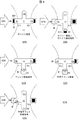
検査装置1は、室温環境にて実施される試験において、あるマウントMを介して第1のインデックステーブル11のデバイス載置領域ADに載置された半導体デバイスDUTが不良品であることが判明したときに、そのマウントMをマウント回収/供給ユニット14より供給された予備マウントM’と交換する機能を有している。このマウント交換方法S200の流れについて、図6を参照して説明する。図6は、マウント交換方法S200の流れを示す模式図である。
検査装置1は、高温環境にて実施される試験において、あるマウントMを介して第2のインデックステーブル12のデバイス載置領域ADに載置された半導体デバイスDUTが不良品であることが判明したときに、そのマウントMを第2のインデックステーブル12のマウント載置領域AMに載置された予備マウントM’と交換する機能を有している。このマウント交換方法S300の流れについて、図7を参照して説明する。図7は、マウント交換方法S300の流れを示す模式図である。
なお、本実施形態においては、第1のテーブル内搬送経路P1上の第2のポジションP12において動特性試験を実施すると共に、第1のテーブル内搬送経路P1上の第4のポジションP14において静特性試験を実施する構成を採用しているが、本発明はこれに限定されない。例えば、第1のテーブル内搬送経路P1上の第2のポジションP12において静特性試験を実施すると共に、第1のテーブル内搬送経路P1上の第4のポジションP14において動特性試験を実施する構成を採用してもよい。ただし、本実施形態に係る構成によれば、動特性試験が最後の試験にならない。このため、本実施形態に係る構成には、動特性試験により生じた半導体デバイスの不具合を後続する試験により検知することが可能になるというメリットがある。
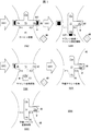
なお、2つのインデックステーブルを備えた検査装置を用いれば、図8の(a)に示すような搬送経路も実現することができる。
また、2つのインデックステーブルを備えた検査装置を用いれば、図8の(b)に示すような搬送経路も実現することができる。
本発明は上述した実施形態に限定されるものではなく、請求項に示した範囲で種々の変更が可能であり、上述した実施形態に開示された各技術的手段を適宜組み合わせて得られる実施形態についても本発明の技術的範囲に含まれる。
11 第1のインデックステーブル
12 第2のインデックステーブル
13 アーム
14 マウント回収/供給ユニット
15 第1の試験装置(室温環境における動特性試験用)
16 第2の試験装置(高温環境における動特性試験用)
17 第3の試験装置(高温環境における静特性試験用)
18 第4の試験装置(室温環境における静特性試験用)
Claims (8)
- 第1のインデックステーブルと、
第2のインデックステーブルと、
前記第1のインデックステーブルと前記第2のインデックステーブルとの間でデバイスを移載するデバイス移載動作を行うアームと、
前記第1のインデックステーブルに載置されたデバイスに対して、第1の環境における試験を実施する第1の試験装置と、
前記第2のインデックステーブルに載置されたデバイスに対して、前記第1の環境とは異なる第2の環境における試験を実施する第2の試験装置と、を備えている、
ことを特徴とする検査装置。 - 前記アームは、前記デバイス移載動作において、第1のポジションにおいて前記第1のインデックステーブルから取得したデバイスを、第2のポジションにおいて前記第2のインデックステーブルに載置し、
前記第1のポジションは、前記第1のインデックステーブルによりデバイスが搬送される第1の搬送経路において、前記第2のインデックステーブルに最も近いポジションであり、
前記第2のポジションは、前記第2のインデックステーブルによりデバイスが搬送される第2の搬送経路において、前記第1のインデックステーブルに最も近いポジションである、
ことを特徴とする請求項1に記載の検査装置。 - 前記アームは、前記デバイス移載動作において、前記第1のポジションにおいて前記第1のインデックステーブルから取得したデバイスを、前記第2のインデックステーブルに載置するのと同時に、前記第2のポジションにおいて前記第2のインデックステーブルから取得したデバイスを、前記第1のインデックステーブルに載置する、
ことを特徴とする請求項2に記載の検査装置。 - 前記第2のインデックステーブルに載置されたデバイスに対して、前記第2の環境における試験を実施する第3の試験装置と、
前記第1のインデックステーブルに載置されたデバイスに対して、前記第1の環境における試験を実施する第4の試験装置と、を更に備えている、
ことを特徴とする請求項1〜3の何れか1項に記載の検査装置。 - 前記第1の試験装置及び前記第4の試験装置の一方は、動特性試験を実施し、他方は、静特性試験を実施し、
前記第2の試験装置及び前記第3の試験装置の一方は、動特性試験を実施し、他方は、静特性試験を実施する、
ことを特徴とする請求項4に記載の検査装置。 - 前記第1の環境及び前記第2の環境の一方は、室温環境であり、他方は、前記室温環境よりも温度の高い高温環境である、
ことを特徴とする請求項1〜5の何れか1項に記載の検査装置。 - 前記第1のインデックステーブル及び前記第2のインデックステーブルのうち、前記高温環境における試験が実施される方のインデックステーブルには、前記高温環境を実現するためのヒータが内蔵されている、
ことを特徴とする請求項6に記載の検査装置。 - 前記デバイスは、半導体デバイスである、
ことを特徴とする請求項1〜7の何れか1項に記載の検査装置。
Priority Applications (5)
| Application Number | Priority Date | Filing Date | Title |
|---|---|---|---|
| JP2019068623A JP2020165902A (ja) | 2019-03-29 | 2019-03-29 | 検査装置 |
| TW109109855A TWI839492B (zh) | 2019-03-29 | 2020-03-24 | 檢查裝置 |
| KR1020200037447A KR102724429B1 (ko) | 2019-03-29 | 2020-03-27 | 검사 장치 |
| CN202010230031.1A CN111830386A (zh) | 2019-03-29 | 2020-03-27 | 检查装置 |
| EP20166360.6A EP3719835B1 (en) | 2019-03-29 | 2020-03-27 | Inspecting device |
Applications Claiming Priority (1)
| Application Number | Priority Date | Filing Date | Title |
|---|---|---|---|
| JP2019068623A JP2020165902A (ja) | 2019-03-29 | 2019-03-29 | 検査装置 |
Publications (1)
| Publication Number | Publication Date |
|---|---|
| JP2020165902A true JP2020165902A (ja) | 2020-10-08 |
Family
ID=70056967
Family Applications (1)
| Application Number | Title | Priority Date | Filing Date |
|---|---|---|---|
| JP2019068623A Pending JP2020165902A (ja) | 2019-03-29 | 2019-03-29 | 検査装置 |
Country Status (5)
| Country | Link |
|---|---|
| EP (1) | EP3719835B1 (ja) |
| JP (1) | JP2020165902A (ja) |
| KR (1) | KR102724429B1 (ja) |
| CN (1) | CN111830386A (ja) |
| TW (1) | TWI839492B (ja) |
Families Citing this family (1)
| Publication number | Priority date | Publication date | Assignee | Title |
|---|---|---|---|---|
| JP7192621B2 (ja) * | 2019-03-29 | 2022-12-20 | 新東工業株式会社 | 検査装置 |
Citations (4)
| Publication number | Priority date | Publication date | Assignee | Title |
|---|---|---|---|---|
| JPH09257873A (ja) * | 1996-03-21 | 1997-10-03 | Hitachi Electron Eng Co Ltd | Icデバイスの加熱装置 |
| JP2001273793A (ja) * | 2000-03-27 | 2001-10-05 | Hiroshima Nippon Denki Kk | 半導体生産システム及び半導体装置の生産方法 |
| JP2003075504A (ja) * | 2001-09-05 | 2003-03-12 | Nec Eng Ltd | 電子部品測定方法および装置 |
| JP2010133716A (ja) * | 2008-12-02 | 2010-06-17 | Ueno Seiki Kk | 高低温化装置及び高低温化装置を備えたテストハンドラ |
Family Cites Families (16)
| Publication number | Priority date | Publication date | Assignee | Title |
|---|---|---|---|---|
| JPS5839021A (ja) * | 1981-08-31 | 1983-03-07 | Nec Home Electronics Ltd | 半導体装置の検査方法 |
| JPH0423446A (ja) | 1990-05-18 | 1992-01-27 | Toshiba Corp | 半導体素子の信頼性評価方法 |
| JPH05333106A (ja) * | 1992-06-03 | 1993-12-17 | Fujitsu Ten Ltd | 温度特性試験装置 |
| JP3563108B2 (ja) * | 1994-05-27 | 2004-09-08 | 株式会社アドバンテスト | Icテストハンドラのデバイス搬送機構 |
| JPH08304509A (ja) * | 1995-04-28 | 1996-11-22 | Advantest Corp | 半導体試験装置 |
| JP4037962B2 (ja) * | 1998-06-24 | 2008-01-23 | 株式会社アドバンテスト | 部品試験装置 |
| JP3925826B2 (ja) * | 1998-07-17 | 2007-06-06 | 株式会社アドバンテスト | 電子部品試験装置 |
| SG98373A1 (en) * | 1998-11-25 | 2003-09-19 | Advantest Corp | Device testing apparatus |
| WO2010010688A1 (ja) * | 2008-07-24 | 2010-01-28 | 株式会社アルバック | 処理装置の作動監視システム |
| JP5461268B2 (ja) * | 2010-03-29 | 2014-04-02 | 日置電機株式会社 | 基板検査システム |
| KR101199718B1 (ko) * | 2011-04-28 | 2012-11-08 | 세크론 주식회사 | 발광 소자 검사 장치 |
| TW201401408A (zh) * | 2012-06-27 | 2014-01-01 | Dah Technology Co Ltd | 晶片移載裝置 |
| TWI475234B (zh) * | 2013-07-18 | 2015-03-01 | Chroma Ate Inc | Inspection machine with fan-shaped turntable transmission equipment |
| US9673076B2 (en) * | 2013-11-05 | 2017-06-06 | Varian Semiconductor Equipment Associates, Inc. | System and method for rotational transfer of articles between vacuum and non-vacuum environments |
| JP6520356B2 (ja) * | 2015-04-28 | 2019-05-29 | 新東工業株式会社 | 検査装置および検査方法 |
| JP6560356B2 (ja) * | 2015-09-29 | 2019-08-14 | 株式会社村田製作所 | 電子部品の検査装置及び検査方法 |
-
2019
- 2019-03-29 JP JP2019068623A patent/JP2020165902A/ja active Pending
-
2020
- 2020-03-24 TW TW109109855A patent/TWI839492B/zh active
- 2020-03-27 KR KR1020200037447A patent/KR102724429B1/ko active Active
- 2020-03-27 EP EP20166360.6A patent/EP3719835B1/en active Active
- 2020-03-27 CN CN202010230031.1A patent/CN111830386A/zh active Pending
Patent Citations (4)
| Publication number | Priority date | Publication date | Assignee | Title |
|---|---|---|---|---|
| JPH09257873A (ja) * | 1996-03-21 | 1997-10-03 | Hitachi Electron Eng Co Ltd | Icデバイスの加熱装置 |
| JP2001273793A (ja) * | 2000-03-27 | 2001-10-05 | Hiroshima Nippon Denki Kk | 半導体生産システム及び半導体装置の生産方法 |
| JP2003075504A (ja) * | 2001-09-05 | 2003-03-12 | Nec Eng Ltd | 電子部品測定方法および装置 |
| JP2010133716A (ja) * | 2008-12-02 | 2010-06-17 | Ueno Seiki Kk | 高低温化装置及び高低温化装置を備えたテストハンドラ |
Also Published As
| Publication number | Publication date |
|---|---|
| TW202102868A (zh) | 2021-01-16 |
| EP3719835A1 (en) | 2020-10-07 |
| CN111830386A (zh) | 2020-10-27 |
| KR102724429B1 (ko) | 2024-10-30 |
| EP3719835B1 (en) | 2022-10-12 |
| TWI839492B (zh) | 2024-04-21 |
| KR20200115347A (ko) | 2020-10-07 |
Similar Documents
| Publication | Publication Date | Title |
|---|---|---|
| TWI442509B (zh) | Check the device | |
| JP4458447B2 (ja) | 電子部品試験用保持装置、電子部品試験装置および電子部品試験方法 | |
| KR20150034230A (ko) | 반도체 검사 시스템 및 인터페이스부의 결로 방지 방법 | |
| CN102257437B (zh) | 预对准装置以及预对准方法 | |
| US20140354312A1 (en) | Test handler, test carrier and test method thereof | |
| KR20210111681A (ko) | 검사 장치 | |
| CN112394207B (zh) | 探针装置和探针卡的预冷却方法 | |
| JP2020165903A (ja) | 検査装置 | |
| JP2020165902A (ja) | 検査装置 | |
| TWI618164B (zh) | 電子零件搬送裝置及電子零件檢查裝置 | |
| JP7192621B2 (ja) | 検査装置 | |
| JP4832151B2 (ja) | プローブカード受け渡し方法、プローバ及びプローブカード供給・回収システム | |
| JP2022177010A (ja) | 搬送ユニット | |
| JP2010175288A (ja) | 電子デバイス検査装置及び電子デバイスを保持する治具 | |
| JP2010175287A (ja) | 電子デバイス検査装置及び電子デバイスの検査方法 | |
| JP2005010068A (ja) | 被検査品の外観検査装置及び外観検査方法 | |
| JP2021168321A (ja) | 部品圧着装置及び部品圧着方法 | |
| JP2016148610A (ja) | 電子部品搬送装置および電子部品検査装置 | |
| CN113050311A (zh) | 部件压接装置以及部件压接方法 | |
| JP2017067594A (ja) | 電子部品搬送装置および電子部品検査装置 | |
| JP2016023993A (ja) | 電子部品搬送装置および電子部品検査装置 | |
| JP5163703B2 (ja) | 部品実装システム及びパネル搬送方法 | |
| JPS6254176A (ja) | 継続処理を可能とする環境試験方法及び装置 | |
| JP2017150965A (ja) | 電子部品搬送装置および電子部品検査装置 |
Legal Events
| Date | Code | Title | Description |
|---|---|---|---|
| A621 | Written request for application examination |
Free format text: JAPANESE INTERMEDIATE CODE: A621 Effective date: 20210513 |
|
| A977 | Report on retrieval |
Free format text: JAPANESE INTERMEDIATE CODE: A971007 Effective date: 20220428 |
|
| A131 | Notification of reasons for refusal |
Free format text: JAPANESE INTERMEDIATE CODE: A131 Effective date: 20220510 |
|
| A521 | Request for written amendment filed |
Free format text: JAPANESE INTERMEDIATE CODE: A523 Effective date: 20220630 |
|
| A02 | Decision of refusal |
Free format text: JAPANESE INTERMEDIATE CODE: A02 Effective date: 20221004 |