JP2020508564A - 基板を接合する方法および装置 - Google Patents
基板を接合する方法および装置 Download PDFInfo
- Publication number
- JP2020508564A JP2020508564A JP2019542366A JP2019542366A JP2020508564A JP 2020508564 A JP2020508564 A JP 2020508564A JP 2019542366 A JP2019542366 A JP 2019542366A JP 2019542366 A JP2019542366 A JP 2019542366A JP 2020508564 A JP2020508564 A JP 2020508564A
- Authority
- JP
- Japan
- Prior art keywords
- substrate
- radiation
- amorphous
- substrates
- layers
- Prior art date
- Legal status (The legal status is an assumption and is not a legal conclusion. Google has not performed a legal analysis and makes no representation as to the accuracy of the status listed.)
- Pending
Links
Images

Classifications
-
- H—ELECTRICITY
- H10—SEMICONDUCTOR DEVICES; ELECTRIC SOLID-STATE DEVICES NOT OTHERWISE PROVIDED FOR
- H10P—GENERIC PROCESSES OR APPARATUS FOR THE MANUFACTURE OR TREATMENT OF DEVICES COVERED BY CLASS H10
- H10P10/00—Bonding of wafers, substrates or parts of devices
- H10P10/12—Bonding of semiconductor wafers or semiconductor substrates to semiconductor wafers or semiconductor substrates
-
- H—ELECTRICITY
- H10—SEMICONDUCTOR DEVICES; ELECTRIC SOLID-STATE DEVICES NOT OTHERWISE PROVIDED FOR
- H10P—GENERIC PROCESSES OR APPARATUS FOR THE MANUFACTURE OR TREATMENT OF DEVICES COVERED BY CLASS H10
- H10P90/00—Preparation of wafers not covered by a single main group of this subclass, e.g. wafer reinforcement
- H10P90/19—Preparing inhomogeneous wafers
- H10P90/1904—Preparing vertically inhomogeneous wafers
- H10P90/1906—Preparing SOI wafers
- H10P90/1914—Preparing SOI wafers using bonding
-
- H—ELECTRICITY
- H10—SEMICONDUCTOR DEVICES; ELECTRIC SOLID-STATE DEVICES NOT OTHERWISE PROVIDED FOR
- H10P—GENERIC PROCESSES OR APPARATUS FOR THE MANUFACTURE OR TREATMENT OF DEVICES COVERED BY CLASS H10
- H10P10/00—Bonding of wafers, substrates or parts of devices
- H10P10/12—Bonding of semiconductor wafers or semiconductor substrates to semiconductor wafers or semiconductor substrates
- H10P10/126—Bonding of semiconductor wafers or semiconductor substrates to semiconductor wafers or semiconductor substrates characterised by the composition of the bonding layer, e.g. dopant concentration or stoichiometry
-
- H—ELECTRICITY
- H10—SEMICONDUCTOR DEVICES; ELECTRIC SOLID-STATE DEVICES NOT OTHERWISE PROVIDED FOR
- H10P—GENERIC PROCESSES OR APPARATUS FOR THE MANUFACTURE OR TREATMENT OF DEVICES COVERED BY CLASS H10
- H10P14/00—Formation of materials, e.g. in the shape of layers or pillars
- H10P14/20—Formation of materials, e.g. in the shape of layers or pillars of semiconductor materials
- H10P14/34—Deposited materials, e.g. layers
- H10P14/3451—Structure
- H10P14/3452—Microstructure
- H10P14/3454—Amorphous
-
- H—ELECTRICITY
- H10—SEMICONDUCTOR DEVICES; ELECTRIC SOLID-STATE DEVICES NOT OTHERWISE PROVIDED FOR
- H10P—GENERIC PROCESSES OR APPARATUS FOR THE MANUFACTURE OR TREATMENT OF DEVICES COVERED BY CLASS H10
- H10P14/00—Formation of materials, e.g. in the shape of layers or pillars
- H10P14/60—Formation of materials, e.g. in the shape of layers or pillars of insulating materials
- H10P14/65—Formation of materials, e.g. in the shape of layers or pillars of insulating materials characterised by treatments performed before or after the formation of the materials
- H10P14/6516—Formation of materials, e.g. in the shape of layers or pillars of insulating materials characterised by treatments performed before or after the formation of the materials of treatments performed after formation of the materials
- H10P14/6544—Formation of materials, e.g. in the shape of layers or pillars of insulating materials characterised by treatments performed before or after the formation of the materials of treatments performed after formation of the materials to change the morphology of the insulating materials, e.g. transformation of an amorphous layer into a crystalline layer
-
- H—ELECTRICITY
- H10—SEMICONDUCTOR DEVICES; ELECTRIC SOLID-STATE DEVICES NOT OTHERWISE PROVIDED FOR
- H10P—GENERIC PROCESSES OR APPARATUS FOR THE MANUFACTURE OR TREATMENT OF DEVICES COVERED BY CLASS H10
- H10P34/00—Irradiation with electromagnetic or particle radiation of wafers, substrates or parts of devices
- H10P34/40—Irradiation with electromagnetic or particle radiation of wafers, substrates or parts of devices with high-energy radiation
- H10P34/42—Irradiation with electromagnetic or particle radiation of wafers, substrates or parts of devices with high-energy radiation with electromagnetic radiation, e.g. laser annealing
-
- H—ELECTRICITY
- H10—SEMICONDUCTOR DEVICES; ELECTRIC SOLID-STATE DEVICES NOT OTHERWISE PROVIDED FOR
- H10P—GENERIC PROCESSES OR APPARATUS FOR THE MANUFACTURE OR TREATMENT OF DEVICES COVERED BY CLASS H10
- H10P72/00—Handling or holding of wafers, substrates or devices during manufacture or treatment thereof
- H10P72/04—Apparatus for manufacture or treatment
- H10P72/0428—Apparatus for mechanical treatment or grinding or cutting
-
- H—ELECTRICITY
- H10—SEMICONDUCTOR DEVICES; ELECTRIC SOLID-STATE DEVICES NOT OTHERWISE PROVIDED FOR
- H10P—GENERIC PROCESSES OR APPARATUS FOR THE MANUFACTURE OR TREATMENT OF DEVICES COVERED BY CLASS H10
- H10P95/00—Generic processes or apparatus for manufacture or treatments not covered by the other groups of this subclass
- H10P95/90—Thermal treatments, e.g. annealing or sintering
-
- H—ELECTRICITY
- H10—SEMICONDUCTOR DEVICES; ELECTRIC SOLID-STATE DEVICES NOT OTHERWISE PROVIDED FOR
- H10W—GENERIC PACKAGES, INTERCONNECTIONS, CONNECTORS OR OTHER CONSTRUCTIONAL DETAILS OF DEVICES COVERED BY CLASS H10
- H10W72/00—Interconnections or connectors in packages
- H10W72/071—Connecting or disconnecting
- H10W72/076—Connecting or disconnecting of strap connectors
Landscapes
- Physics & Mathematics (AREA)
- Recrystallisation Techniques (AREA)
- Chemical & Material Sciences (AREA)
- Crystallography & Structural Chemistry (AREA)
- Electromagnetism (AREA)
- Optics & Photonics (AREA)
- Pressure Welding/Diffusion-Bonding (AREA)
- Laminated Bodies (AREA)
- Health & Medical Sciences (AREA)
- High Energy & Nuclear Physics (AREA)
- Toxicology (AREA)
Abstract
Description
第1の非晶質層を第1の基板上に形成する、かつ/または第2の非晶質層を第2の基板上に形成するステップと、
第1の基板を第2の基板に、1つのまたは複数の非晶質層で接続し、基板積層体を形成するステップと、
1つのまたは複数の非晶質層を、1つのまたは複数の非晶質層が、1つのまたは複数の結晶層に転移するように、放射により照射するステップと、
を有している方法が提供される。
基板を保持するための保持装置と、
基板を接合するための接合装置と、
照射装置と、
を有しており、
第1の非晶質層を第1の基板上に形成可能であり、かつ/または第2の非晶質層を第2の基板上に形成可能であり、
第1の基板を第2の基板に、1つのまたは複数の非晶質層で接続して、基板積層体を形成可能であり、
1つのまたは複数の非晶質層を、1つのまたは複数の非晶質層が、1つのまたは複数の結晶層に転移可能であるように、放射装置により放射を照射可能であるように、形成されている、
装置が提供される。
−化学気相成長(CVD)、
−物理気相成長(PVD)、
−プラズマ処理、または
−イオンビーム処理。
−接合すべき基板表面に非晶質化層を製作するステップ、
−基板表面を清浄化するステップ、
−基板を互いに位置合わせするステップ、
−直接接合により予備接合するステップ、
−接合境界面を離間するために本発明によりレーザー処理するステップ。
−材料:SEMI規格および別の規定による形状許容差および位置許容差を含む基板ジオメトリ、基板の平坦性ならびにうねり、基板材料、ドーピング、非晶質化、非晶質層の層厚さ、
−材料の組み合わせ:同一の非晶質層を有するが、基板体積(英語:bulk)において異なる材料を有する基板が接合される場合、または基板が実質的に互いに同一である場合、
−基板の準備:基板の清浄性、異種原子負荷、接合すべき面上ならびに境界層における原子状の水の層または気体の導入、
−波長、作用期間、入射角度を伴う放射の放射入力、
−基板積層体のための周辺条件:温度、大気。
・原子吸光分光法(AAS)
・原子発光分光法(AES)
・エネルギ分散型X線分光法(EDX)
・波長分散型X線分光法(WDX)
・スパーク放電発光分光法(OES)
・蛍光法
○原子蛍光分光法(AFS)
○X線蛍光分析法(XRF)
以下に、本発明の例示的な方法を説明する。
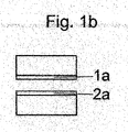
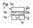
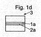
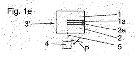
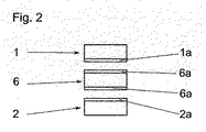
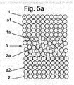
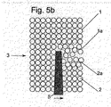
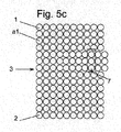
1a 第1の基板の第1の非晶質層
1o 第1の層の接合表面
2 第2の基板
2a 第2の基板の第2の非晶質層
2o 第2の層の接合表面
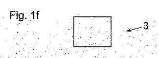
3 基板積層体
4 放射の放射源
5 放射
6 第3の基板
6a 第3の基板の非晶質層
7 転位
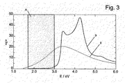
8,9 吸収スペクトル
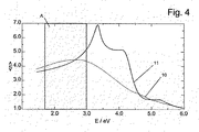
10,11 屈折率グラフ
a1,a2 原子
A 粒子エネルギ範囲
ε 吸収率
n 屈折率
P 移動矢印
Claims (16)
- 第1の基板(1,6)を第2の基板(2)に接合する方法であって、
第1の非晶質層(1a,6a)を前記第1の基板(1,6)上に形成する、かつ/または第2の非晶質層(2a)を前記第2の基板(2)上に形成するステップと、
前記第1の基板(1,6)を前記第2の基板(2)に、1つのまたは複数の前記非晶質層(1a,2a,6a)で接続し、基板積層体(3)を形成するステップと、
前記1つのまたは複数の非晶質層(1a,2a,6a)が1つのまたは複数の結晶層に転移するように、前記1つのまたは複数の非晶質層(1a,2a,6a)を、放射(5)により照射するステップと、
を有する、第1の基板(1,6)を第2の基板(2)に接合する方法。 - 前記1つのまたは複数の非晶質層(1a,2a,6a)を大部分、好適には完全に、1つのまたは複数の結晶層に転移させる、請求項1記載の方法。
- 1つのまたは複数の前記基板(1,2,6)の接合表面(1o,2o)の殆どの部分に1つの非晶質層(1a,2a,6a)を形成し、好適には前記1つのまたは複数の基板(1,2,6)の接合表面(1o,2o)全体に1つの非晶質層(1a,2a,6a)を形成する、請求項1または2記載の方法。
- 前記基板(1,2,6)のうちの少なくとも1つは、前記放射(5)に対して透過性であり、前記放射(5)の放射エネルギの少なくとも50%が、好適には少なくとも60%が、特に好適には少なくとも70%が、極めて特に好適には少なくとも80%が、さらに好適には少なくとも90%が透過される、請求項1から3までのいずれか1項記載の方法。
- 前記非晶質層(1a,2a,6a)によって前記放射(5)を、前記放射(5)の放射エネルギの60%超まで、好適には60%超まで、さらに好適には70%超まで、特に好適には80%超まで、極めて特に好適には90%超まで、吸収する、請求項1から4までのいずれか1項記載の方法。
- 前記放射(5)はレーザー放射であり、前記レーザー放射を前記非晶質層(1a,2a,6a)へと収束させる、請求項1から5までのいずれか1項記載の方法。
- 前記放射(5)は、前記非晶質層(1a,2a,6a)に垂直に当てられる、請求項1から6までのいずれか1項記載の方法。
- 前記放射(5)を、1eV〜10E8eVの、好適には1eV〜10E6eVの、さらに好適には1eV〜10E4eVの、最も好適には1eV〜10eVのエネルギ範囲で放射する広帯域エミッタによって発生させる、請求項1から7までのいずれか1項記載の方法。
- 前記放射(5)の放射出力は、0.01ワット〜10000ワットであって、好適には0.1ワット〜1000ワットであって、最も好適には1ワット〜100ワットである、請求項1から8までのいずれか1項記載の方法。
- 前記放射(5)により、前記1つのまたは複数の非晶質層(1a,2a,6a)に、200℃超の、好適には400℃超の、特に好適には600℃超の、さらに好適には800℃超の、最も好適には1200℃超の温度を発生させる、請求項1から9までのいずれか1項記載の方法。
- 入射時間は、30秒未満であり、好適には15秒未満であり、特に好適には1秒未満であり、極めて特に好適には100ミリ秒未満である、請求項1から10までのいずれか1項記載の方法。
- 基板面および/または基板積層体面での前記放射(5)の反射は、放射源(4)の出力強度の4%未満であり、好適には3%未満であり、特に好適には1%未満である、請求項1から11までのいずれか1項記載の方法。
- 前記第1の基板(1,6)および/または前記第2の基板(2)は、前記放射(5)に対して、放射源(4)の出力強度の少なくとも95%透過性であり、好適には97%透過性であり、特に好適には99%透過性である、請求項1から12までのいずれか1項記載の方法。
- 照射前および/または照射中、前記基板(1,2,6)の少なくとも一方の基板の、好適には両方の基板(1,2,6)の加熱を行い、この場合、前記1つのまたは複数の基板(1,2,6)を、100℃を超えるように、好適には200℃を超えるように、特に好適には300℃を超えるように加熱する、請求項1から13までのいずれか1項記載の方法。
- 特に請求項1から14までのいずれか1項記載の方法により、第1の基板(1,6)を第2の基板(2)に接合する装置であって、
前記基板(1,2,6)を保持するための保持装置と、
前記基板(1,2,6)を接合するための接合装置と、
照射装置(4)と、
を有しており、
第1の非晶質層(1a,6a)を前記第1の基板(1,6)上に形成可能であり、かつ/または第2の非晶質層(2a)を前記第2の基板(2)上に形成可能であり、
前記第1の基板(1,6)を前記第2の基板(2)に、1つのまたは複数の前記非晶質層(1a,2a,6a)で接続して、基板積層体(3)を形成可能であり、
前記1つのまたは複数の非晶質層(1a,2a,6a)が、1つのまたは複数の結晶層に転移可能であるように、前記照射装置(4)により前記1つのまたは複数の非晶質層(1a,2a,6a)に放射(5)を照射可能である
ように、形成されている、第1の基板(1,6)を第2の基板(2)に接合する装置。 - 請求項1から14までのいずれか1項記載の方法および/または請求項15記載の装置によって接合された少なくとも1つの第1の基板(1,6)と少なくとも1つの第2の基板(2)とによって形成される基板積層体(3)。
Applications Claiming Priority (1)
| Application Number | Priority Date | Filing Date | Title |
|---|---|---|---|
| PCT/EP2017/053918 WO2018153434A1 (de) | 2017-02-21 | 2017-02-21 | Verfahren und vorrichtung zum bonden von substraten |
Publications (1)
| Publication Number | Publication Date |
|---|---|
| JP2020508564A true JP2020508564A (ja) | 2020-03-19 |
Family
ID=58108607
Family Applications (1)
| Application Number | Title | Priority Date | Filing Date |
|---|---|---|---|
| JP2019542366A Pending JP2020508564A (ja) | 2017-02-21 | 2017-02-21 | 基板を接合する方法および装置 |
Country Status (7)
| Country | Link |
|---|---|
| US (2) | US10971365B2 (ja) |
| EP (1) | EP3586356B1 (ja) |
| JP (1) | JP2020508564A (ja) |
| KR (1) | KR102615398B1 (ja) |
| CN (1) | CN110235223A (ja) |
| SG (1) | SG11201906390SA (ja) |
| WO (1) | WO2018153434A1 (ja) |
Cited By (3)
| Publication number | Priority date | Publication date | Assignee | Title |
|---|---|---|---|---|
| JP2024021511A (ja) * | 2022-08-03 | 2024-02-16 | 株式会社Sumco | 接合シリコンウェーハ及びその製造方法 |
| WO2025109948A1 (ja) * | 2023-11-22 | 2025-05-30 | 株式会社サイコックス | 接合半導体基板および接合半導体基板の製造方法 |
| WO2025109949A1 (ja) * | 2023-11-22 | 2025-05-30 | 株式会社サイコックス | 接合半導体基板および接合半導体基板の製造方法 |
Families Citing this family (2)
| Publication number | Priority date | Publication date | Assignee | Title |
|---|---|---|---|---|
| US12457751B2 (en) | 2021-07-19 | 2025-10-28 | Taiwan Semiconductor Manufacturing Company, Ltd. | Interfacial layer with high texture uniformity for ferroelectric layer enhancement |
| FR3165103A1 (fr) * | 2024-07-25 | 2026-01-30 | Commissariat A L' Energie Atomique Et Aux Energies Alternatives | Procédé de collage covalent par diffusion atomique pour former une interface de collage conductrice |
Citations (3)
| Publication number | Priority date | Publication date | Assignee | Title |
|---|---|---|---|---|
| JPH04180674A (ja) * | 1990-01-10 | 1992-06-26 | Ricoh Co Ltd | 半導体膜の製造方法 |
| JP2015220320A (ja) * | 2014-05-16 | 2015-12-07 | 株式会社豊田自動織機 | 半導体基板の製造方法 |
| US20170025306A1 (en) * | 2015-07-21 | 2017-01-26 | Sunedison Semiconductor Limited (Uen201334164H) | Methods for preparing layered semiconductor structures and related bonded structures |
Family Cites Families (37)
| Publication number | Priority date | Publication date | Assignee | Title |
|---|---|---|---|---|
| US5441776A (en) | 1993-11-08 | 1995-08-15 | Sterling; Rodney D. | Silicon dioxide bonding layers and method |
| US20010045352A1 (en) * | 1998-05-14 | 2001-11-29 | Robinson Raymond S. | Sputter deposition using multiple targets |
| US6534381B2 (en) * | 1999-01-08 | 2003-03-18 | Silicon Genesis Corporation | Method for fabricating multi-layered substrates |
| US6881644B2 (en) * | 1999-04-21 | 2005-04-19 | Silicon Genesis Corporation | Smoothing method for cleaved films made using a release layer |
| JP4450126B2 (ja) * | 2000-01-21 | 2010-04-14 | 日新電機株式会社 | シリコン系結晶薄膜の形成方法 |
| FR2817395B1 (fr) * | 2000-11-27 | 2003-10-31 | Soitec Silicon On Insulator | Procede de fabrication d'un substrat notamment pour l'optique, l'electronique ou l'optoelectronique et substrat obtenu par ce procede |
| US6497763B2 (en) * | 2001-01-19 | 2002-12-24 | The United States Of America As Represented By The Secretary Of The Navy | Electronic device with composite substrate |
| WO2003097552A1 (en) * | 2002-04-30 | 2003-11-27 | Agency For Science Technology And Research | A method of wafer/substrate bonding |
| JP3774782B2 (ja) * | 2003-05-14 | 2006-05-17 | 富士通メディアデバイス株式会社 | 弾性表面波素子の製造方法 |
| US7165712B2 (en) * | 2003-10-23 | 2007-01-23 | Siemens Power Generation, Inc. | Transient liquid phase bonding to cold-worked surfaces |
| JP2005288673A (ja) * | 2004-04-06 | 2005-10-20 | Mitsubishi Heavy Ind Ltd | 微小構造体の製造装置 |
| US7410882B2 (en) * | 2004-09-28 | 2008-08-12 | Palo Alto Research Center Incorporated | Method of manufacturing and structure of polycrystalline semiconductor thin-film heterostructures on dissimilar substrates |
| US7565996B2 (en) * | 2004-10-04 | 2009-07-28 | United Technologies Corp. | Transient liquid phase bonding using sandwich interlayers |
| JP2006187685A (ja) * | 2004-12-28 | 2006-07-20 | Fuji Xerox Co Ltd | 微小構造体、マイクロリアクタ、熱交換器、および微小構造体の製造方法 |
| US8138061B2 (en) * | 2005-01-07 | 2012-03-20 | International Business Machines Corporation | Quasi-hydrophobic Si-Si wafer bonding using hydrophilic Si surfaces and dissolution of interfacial bonding oxide |
| JP4934966B2 (ja) * | 2005-02-04 | 2012-05-23 | 株式会社Sumco | Soi基板の製造方法 |
| US7462552B2 (en) * | 2005-05-23 | 2008-12-09 | Ziptronix, Inc. | Method of detachable direct bonding at low temperatures |
| US20080035707A1 (en) * | 2006-08-14 | 2008-02-14 | The Regents Of The University Of California | Transient-liquid-phase joining of ceramics at low temperatures |
| JP4172806B2 (ja) * | 2006-09-06 | 2008-10-29 | 三菱重工業株式会社 | 常温接合方法及び常温接合装置 |
| US8993410B2 (en) * | 2006-09-08 | 2015-03-31 | Silicon Genesis Corporation | Substrate cleaving under controlled stress conditions |
| FR2921749B1 (fr) * | 2007-09-27 | 2014-08-29 | Soitec Silicon On Insulator | Procede de fabrication d'une structure comprenant un substrat et une couche deposee sur l'une de ses faces. |
| KR101499175B1 (ko) * | 2007-10-04 | 2015-03-05 | 가부시키가이샤 한도오따이 에네루기 켄큐쇼 | 반도체 기판의 제조방법 |
| FR2938120B1 (fr) * | 2008-10-31 | 2011-04-08 | Commissariat Energie Atomique | Procede de formation d'une couche monocristalline dans le domaine micro-electronique |
| SG162675A1 (en) * | 2008-12-15 | 2010-07-29 | Semiconductor Energy Lab | Manufacturing method of soi substrate and manufacturing method of semiconductor device |
| US8247317B2 (en) * | 2009-09-16 | 2012-08-21 | Applied Materials, Inc. | Methods of solid phase recrystallization of thin film using pulse train annealing method |
| JP5889411B2 (ja) | 2011-08-30 | 2016-03-22 | エーファウ・グループ・エー・タルナー・ゲーエムベーハー | 固相拡散または相変態を用いた接続層による恒久的なウエハ結合方法 |
| US9492990B2 (en) * | 2011-11-08 | 2016-11-15 | Picosys Incorporated | Room temperature glass-to-glass, glass-to-plastic and glass-to-ceramic/semiconductor bonding |
| FR2983342B1 (fr) * | 2011-11-30 | 2016-05-20 | Soitec Silicon On Insulator | Procede de fabrication d'une heterostructure limitant la formation de defauts et heterostructure ainsi obtenue |
| EP2822026B1 (en) * | 2012-02-29 | 2018-03-14 | Kyocera Corporation | Composite substrate |
| FR2995445B1 (fr) * | 2012-09-07 | 2016-01-08 | Soitec Silicon On Insulator | Procede de fabrication d'une structure en vue d'une separation ulterieure |
| US9315417B2 (en) | 2013-02-17 | 2016-04-19 | Invenias Inc | Attachment of a cap to a substrate-based device with in situ monitoring of bond quality |
| JP6061251B2 (ja) * | 2013-07-05 | 2017-01-18 | 株式会社豊田自動織機 | 半導体基板の製造方法 |
| KR102158960B1 (ko) | 2013-07-05 | 2020-09-23 | 에베 그룹 에. 탈너 게엠베하 | 접촉면의 본딩을 위한 방법 |
| EP3127141B1 (de) | 2014-04-01 | 2021-03-24 | EV Group E. Thallner GmbH | Verfahren zur oberflächenreinigung von substraten |
| SG11201608357XA (en) | 2014-06-09 | 2016-11-29 | Dirtt Environmental Solutions | Associating computer-executable objects with timber frames within an architectural design environment |
| US10083854B2 (en) | 2014-06-24 | 2018-09-25 | Ev Group E. Thallner Gmbh | Method and device for surface treatment of substrates |
| US20180104765A1 (en) * | 2016-10-13 | 2018-04-19 | United Technologies Corporation | Hybrid component and method of making |
-
2017
- 2017-02-21 JP JP2019542366A patent/JP2020508564A/ja active Pending
- 2017-02-21 KR KR1020197022649A patent/KR102615398B1/ko active Active
- 2017-02-21 US US16/481,994 patent/US10971365B2/en active Active
- 2017-02-21 EP EP17706731.1A patent/EP3586356B1/de active Active
- 2017-02-21 SG SG11201906390SA patent/SG11201906390SA/en unknown
- 2017-02-21 WO PCT/EP2017/053918 patent/WO2018153434A1/de not_active Ceased
- 2017-02-21 CN CN201780085913.XA patent/CN110235223A/zh active Pending
-
2021
- 2021-02-12 US US17/174,692 patent/US11862466B2/en active Active
Patent Citations (3)
| Publication number | Priority date | Publication date | Assignee | Title |
|---|---|---|---|---|
| JPH04180674A (ja) * | 1990-01-10 | 1992-06-26 | Ricoh Co Ltd | 半導体膜の製造方法 |
| JP2015220320A (ja) * | 2014-05-16 | 2015-12-07 | 株式会社豊田自動織機 | 半導体基板の製造方法 |
| US20170025306A1 (en) * | 2015-07-21 | 2017-01-26 | Sunedison Semiconductor Limited (Uen201334164H) | Methods for preparing layered semiconductor structures and related bonded structures |
Cited By (4)
| Publication number | Priority date | Publication date | Assignee | Title |
|---|---|---|---|---|
| JP2024021511A (ja) * | 2022-08-03 | 2024-02-16 | 株式会社Sumco | 接合シリコンウェーハ及びその製造方法 |
| JP7782388B2 (ja) | 2022-08-03 | 2025-12-09 | 株式会社Sumco | 接合シリコンウェーハ及びその製造方法 |
| WO2025109948A1 (ja) * | 2023-11-22 | 2025-05-30 | 株式会社サイコックス | 接合半導体基板および接合半導体基板の製造方法 |
| WO2025109949A1 (ja) * | 2023-11-22 | 2025-05-30 | 株式会社サイコックス | 接合半導体基板および接合半導体基板の製造方法 |
Also Published As
| Publication number | Publication date |
|---|---|
| US20190393037A1 (en) | 2019-12-26 |
| US20210202251A1 (en) | 2021-07-01 |
| CN110235223A (zh) | 2019-09-13 |
| EP3586356A1 (de) | 2020-01-01 |
| SG11201906390SA (en) | 2019-08-27 |
| KR20190117507A (ko) | 2019-10-16 |
| WO2018153434A1 (de) | 2018-08-30 |
| EP3586356B1 (de) | 2023-11-08 |
| US10971365B2 (en) | 2021-04-06 |
| KR102615398B1 (ko) | 2023-12-18 |
| US11862466B2 (en) | 2024-01-02 |
Similar Documents
| Publication | Publication Date | Title |
|---|---|---|
| US11862466B2 (en) | Method and device for bonding substrates | |
| JP6061251B2 (ja) | 半導体基板の製造方法 | |
| US10297479B2 (en) | Wafer debonding using mid-wavelength infrared radiation ablation | |
| US9586291B2 (en) | Adhesives for bonding handler wafers to device wafers and enabling mid-wavelength infrared laser ablation release | |
| US8101490B2 (en) | Method for manufacturing semiconductor device and apparatus for manufacturing same | |
| US9336989B2 (en) | Method of cleaving a thin sapphire layer from a bulk material by implanting a plurality of particles and performing a controlled cleaving process | |
| CN111373508B (zh) | 用于经减薄的碳化硅器件中欧姆触点的方法和组件 | |
| JP6152827B2 (ja) | 半導体基板の製造方法 | |
| JP5918160B2 (ja) | ゲッタリング半導体ウエハおよびその製造方法 | |
| TWI762469B (zh) | 利用局部電磁波退火移除接合基板內未接合區域之裝置及方法 | |
| US20220367190A1 (en) | Non-contact processing device and processing method | |
| KR20250162533A (ko) | 반도체 기판의 제조방법, 반도체 기판, 및 반도체 장치 | |
| TW200818321A (en) | Semiconductor on insulator structure made using radiation annealing | |
| JP7420922B2 (ja) | 接合基板 | |
| Rasheed et al. | A Review: Laser Annealing of Active SiC and Its Applications | |
| WO2009131061A1 (ja) | Si(1-v-w-x)CwAlxNv基材の製造方法、エピタキシャルウエハの製造方法、Si(1-v-w-x)CwAlxNv基材およびエピタキシャルウエハ | |
| Kupo et al. | Features of diamond crystal processing by pulsed laser radiation in microelectronics technologies | |
| JP5738145B2 (ja) | Soiウェーハの製造方法 | |
| JP2013106024A (ja) | シリコン基板及びその製造方法、並びに、半導体デバイスの製造方法 |
Legal Events
| Date | Code | Title | Description |
|---|---|---|---|
| A621 | Written request for application examination |
Free format text: JAPANESE INTERMEDIATE CODE: A621 Effective date: 20200207 |
|
| A977 | Report on retrieval |
Free format text: JAPANESE INTERMEDIATE CODE: A971007 Effective date: 20210114 |
|
| A131 | Notification of reasons for refusal |
Free format text: JAPANESE INTERMEDIATE CODE: A131 Effective date: 20210301 |
|
| A521 | Request for written amendment filed |
Free format text: JAPANESE INTERMEDIATE CODE: A523 Effective date: 20210527 |
|
| A02 | Decision of refusal |
Free format text: JAPANESE INTERMEDIATE CODE: A02 Effective date: 20210914 |