JP2021027059A - 電子部品モジュール - Google Patents
電子部品モジュール Download PDFInfo
- Publication number
- JP2021027059A JP2021027059A JP2019140663A JP2019140663A JP2021027059A JP 2021027059 A JP2021027059 A JP 2021027059A JP 2019140663 A JP2019140663 A JP 2019140663A JP 2019140663 A JP2019140663 A JP 2019140663A JP 2021027059 A JP2021027059 A JP 2021027059A
- Authority
- JP
- Japan
- Prior art keywords
- electronic component
- substrate
- positioning
- electrode pads
- component
- Prior art date
- Legal status (The legal status is an assumption and is not a legal conclusion. Google has not performed a legal analysis and makes no representation as to the accuracy of the status listed.)
- Granted
Links
Images




Classifications
-
- H—ELECTRICITY
- H10—SEMICONDUCTOR DEVICES; ELECTRIC SOLID-STATE DEVICES NOT OTHERWISE PROVIDED FOR
- H10W—GENERIC PACKAGES, INTERCONNECTIONS, CONNECTORS OR OTHER CONSTRUCTIONAL DETAILS OF DEVICES COVERED BY CLASS H10
- H10W70/00—Package substrates; Interposers; Redistribution layers [RDL]
- H10W70/60—Insulating or insulated package substrates; Interposers; Redistribution layers
- H10W70/62—Insulating or insulated package substrates; Interposers; Redistribution layers characterised by their interconnections
- H10W70/65—Shapes or dispositions of interconnections
-
- H—ELECTRICITY
- H10—SEMICONDUCTOR DEVICES; ELECTRIC SOLID-STATE DEVICES NOT OTHERWISE PROVIDED FOR
- H10W—GENERIC PACKAGES, INTERCONNECTIONS, CONNECTORS OR OTHER CONSTRUCTIONAL DETAILS OF DEVICES COVERED BY CLASS H10
- H10W72/00—Interconnections or connectors in packages
- H10W72/071—Connecting or disconnecting
- H10W72/073—Connecting or disconnecting of die-attach connectors
- H10W72/07321—Aligning
- H10W72/07327—Aligning involving guiding structures, e.g. spacers or supporting members
-
- H—ELECTRICITY
- H10—SEMICONDUCTOR DEVICES; ELECTRIC SOLID-STATE DEVICES NOT OTHERWISE PROVIDED FOR
- H10W—GENERIC PACKAGES, INTERCONNECTIONS, CONNECTORS OR OTHER CONSTRUCTIONAL DETAILS OF DEVICES COVERED BY CLASS H10
- H10W72/00—Interconnections or connectors in packages
- H10W72/071—Connecting or disconnecting
- H10W72/073—Connecting or disconnecting of die-attach connectors
- H10W72/07331—Connecting techniques
- H10W72/07337—Connecting techniques using a polymer adhesive, e.g. an adhesive based on silicone or epoxy
- H10W72/07338—Connecting techniques using a polymer adhesive, e.g. an adhesive based on silicone or epoxy hardening the adhesive by curing, e.g. thermosetting
-
- H—ELECTRICITY
- H10—SEMICONDUCTOR DEVICES; ELECTRIC SOLID-STATE DEVICES NOT OTHERWISE PROVIDED FOR
- H10W—GENERIC PACKAGES, INTERCONNECTIONS, CONNECTORS OR OTHER CONSTRUCTIONAL DETAILS OF DEVICES COVERED BY CLASS H10
- H10W72/00—Interconnections or connectors in packages
- H10W72/071—Connecting or disconnecting
- H10W72/074—Connecting or disconnecting of anisotropic conductive adhesives
-
- H—ELECTRICITY
- H10—SEMICONDUCTOR DEVICES; ELECTRIC SOLID-STATE DEVICES NOT OTHERWISE PROVIDED FOR
- H10W—GENERIC PACKAGES, INTERCONNECTIONS, CONNECTORS OR OTHER CONSTRUCTIONAL DETAILS OF DEVICES COVERED BY CLASS H10
- H10W72/00—Interconnections or connectors in packages
- H10W72/20—Bump connectors, e.g. solder bumps or copper pillars; Dummy bumps; Thermal bumps
- H10W72/231—Shapes
- H10W72/232—Plan-view shape, i.e. in top view
-
- H—ELECTRICITY
- H10—SEMICONDUCTOR DEVICES; ELECTRIC SOLID-STATE DEVICES NOT OTHERWISE PROVIDED FOR
- H10W—GENERIC PACKAGES, INTERCONNECTIONS, CONNECTORS OR OTHER CONSTRUCTIONAL DETAILS OF DEVICES COVERED BY CLASS H10
- H10W72/00—Interconnections or connectors in packages
- H10W72/20—Bump connectors, e.g. solder bumps or copper pillars; Dummy bumps; Thermal bumps
- H10W72/241—Dispositions, e.g. layouts
- H10W72/247—Dispositions of multiple bumps
- H10W72/248—Top-view layouts, e.g. mirror arrays
-
- H—ELECTRICITY
- H10—SEMICONDUCTOR DEVICES; ELECTRIC SOLID-STATE DEVICES NOT OTHERWISE PROVIDED FOR
- H10W—GENERIC PACKAGES, INTERCONNECTIONS, CONNECTORS OR OTHER CONSTRUCTIONAL DETAILS OF DEVICES COVERED BY CLASS H10
- H10W72/00—Interconnections or connectors in packages
- H10W72/30—Die-attach connectors
- H10W72/321—Structures or relative sizes of die-attach connectors
- H10W72/325—Die-attach connectors having a filler embedded in a matrix
-
- H—ELECTRICITY
- H10—SEMICONDUCTOR DEVICES; ELECTRIC SOLID-STATE DEVICES NOT OTHERWISE PROVIDED FOR
- H10W—GENERIC PACKAGES, INTERCONNECTIONS, CONNECTORS OR OTHER CONSTRUCTIONAL DETAILS OF DEVICES COVERED BY CLASS H10
- H10W72/00—Interconnections or connectors in packages
- H10W72/30—Die-attach connectors
- H10W72/351—Materials of die-attach connectors
- H10W72/352—Materials of die-attach connectors comprising metals or metalloids, e.g. solders
-
- H—ELECTRICITY
- H10—SEMICONDUCTOR DEVICES; ELECTRIC SOLID-STATE DEVICES NOT OTHERWISE PROVIDED FOR
- H10W—GENERIC PACKAGES, INTERCONNECTIONS, CONNECTORS OR OTHER CONSTRUCTIONAL DETAILS OF DEVICES COVERED BY CLASS H10
- H10W72/00—Interconnections or connectors in packages
- H10W72/30—Die-attach connectors
- H10W72/351—Materials of die-attach connectors
- H10W72/353—Materials of die-attach connectors not comprising solid metals or solid metalloids, e.g. ceramics
- H10W72/354—Materials of die-attach connectors not comprising solid metals or solid metalloids, e.g. ceramics comprising polymers
-
- H—ELECTRICITY
- H10—SEMICONDUCTOR DEVICES; ELECTRIC SOLID-STATE DEVICES NOT OTHERWISE PROVIDED FOR
- H10W—GENERIC PACKAGES, INTERCONNECTIONS, CONNECTORS OR OTHER CONSTRUCTIONAL DETAILS OF DEVICES COVERED BY CLASS H10
- H10W72/00—Interconnections or connectors in packages
- H10W72/30—Die-attach connectors
- H10W72/381—Auxiliary members
- H10W72/385—Alignment aids, e.g. alignment marks
-
- H—ELECTRICITY
- H10—SEMICONDUCTOR DEVICES; ELECTRIC SOLID-STATE DEVICES NOT OTHERWISE PROVIDED FOR
- H10W—GENERIC PACKAGES, INTERCONNECTIONS, CONNECTORS OR OTHER CONSTRUCTIONAL DETAILS OF DEVICES COVERED BY CLASS H10
- H10W74/00—Encapsulations, e.g. protective coatings
- H10W74/10—Encapsulations, e.g. protective coatings characterised by their shape or disposition
- H10W74/15—Encapsulations, e.g. protective coatings characterised by their shape or disposition on active surfaces of flip-chip devices, e.g. underfills
-
- H—ELECTRICITY
- H10—SEMICONDUCTOR DEVICES; ELECTRIC SOLID-STATE DEVICES NOT OTHERWISE PROVIDED FOR
- H10W—GENERIC PACKAGES, INTERCONNECTIONS, CONNECTORS OR OTHER CONSTRUCTIONAL DETAILS OF DEVICES COVERED BY CLASS H10
- H10W78/00—Detachable holders for supporting packaged chips in operation
-
- H—ELECTRICITY
- H10—SEMICONDUCTOR DEVICES; ELECTRIC SOLID-STATE DEVICES NOT OTHERWISE PROVIDED FOR
- H10W—GENERIC PACKAGES, INTERCONNECTIONS, CONNECTORS OR OTHER CONSTRUCTIONAL DETAILS OF DEVICES COVERED BY CLASS H10
- H10W90/00—Package configurations
- H10W90/701—Package configurations characterised by the relative positions of pads or connectors relative to package parts
- H10W90/731—Package configurations characterised by the relative positions of pads or connectors relative to package parts of die-attach connectors
- H10W90/734—Package configurations characterised by the relative positions of pads or connectors relative to package parts of die-attach connectors between a chip and a stacked insulating package substrate, interposer or RDL
Landscapes
- Electric Connection Of Electric Components To Printed Circuits (AREA)
- Structures For Mounting Electric Components On Printed Circuit Boards (AREA)
- Physics & Mathematics (AREA)
- Geometry (AREA)
- Wire Bonding (AREA)
Abstract
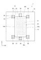
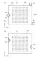
【解決手段】少なくとも1つの位置決め部品が、基板の表面に設けられた金属パッドに固定され、電子部品に向き合う。電子部品と位置決め部品の面内方向の間隙が、前記複数の電極パッドの最小距離より小さい。
【選択図】図1
Description
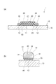
図2(a)は、電子部品モジュール1の模式断面図であり、図2(b)は図2(a)に示す位置決め部品30の拡大断面図である。
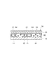
図3は、電子部品20と基板10との接続部の模式断面図である。
Claims (9)
- 基板と、
前記基板の表面に設けられた複数の電極パッドと、
前記基板の表面に設けられた少なくとも1つの金属パッドと、
前記基板の前記表面に搭載される電子部品であって、前記複数の電極パッドの前記表面方向に対向し、且つ前記複数の電極パッドと電気接続される複数の対向電極を有する電子部品と、
前記金属パッドに固定された少なくとも1つの位置決め部品と、
を備え、
前記位置決め部品と前記電子部品の前記基板の前記表面面内方向の間隙が、前記複数の電極パッドの最小距離より短い電子部品モジュール。 - 前記位置決め部品の前記金属パッドに向き合う面に金属膜が設けられ、
前記位置決め部品がはんだで前記金属パッドに固定されている請求項1記載の電子部品モジュール。 - 前記電極パッドと前記金属パッドが、同じ材料、且つ同じ厚さである請求項1または2に記載の電子部品モジュール。
- 前記金属パッドが、前記基板の前記表面に設けられた孤立パターンである、または半田レジストにより開口制限されている請求項3に記載の電子部品モジュール。
- 前記位置決め部品が、前記電子部品に向き合う側面と、上面と、前記側面と前記上面の間に設けられ前記側面および前記上面に対し傾斜した傾斜面と、を有する請求項1〜4のいずれか1つに記載の電子部品モジュール。
- 基板と、
前記基板の表面に設けられた複数の電極パッドと、
前記基板の表面に設けられ、前記基板の前記表面において互いを結ぶ線が三角形を含む配置関係にある少なくとも3つの金属パッドと、
前記基板の前記表面に搭載される電子部品であって、前記複数の電極パッドの前記表面方向に対向し、且つ前記複数の電極パッドと電気接続される複数の対向電極を有する電子部品と、
前記金属パッドにそれぞれ固定された少なくとも3つの位置決め部品と、
を備え、
前記位置決め部品と前記電子部品の前記基板の前記表面面内方向の間隙が、前記複数の電極パッドの最小距離より短い電子部品モジュール。 - 前記位置決め部品の側面が前記電子部品に向き合っている部分が3つ以上である請求項1〜6のいずれか1つに記載の電子部品モジュール。
- 前記電子部品の前記複数の対向電極と、前記複数の電極パッドとの間に設けられ、前記複数の対向電極と前記複数の電極パッドとを電気接続する異方導電性部材をさらに備えた請求項1〜7のいずれか1つに記載の電子部品モジュール。
- 前記電子部品を前記基板の前記表面に向けて押圧する押圧部材をさらに備えた請求項1〜8のいずれか1つに記載の電子部品モジュール。
Priority Applications (2)
| Application Number | Priority Date | Filing Date | Title |
|---|---|---|---|
| JP2019140663A JP7225052B2 (ja) | 2019-07-31 | 2019-07-31 | 電子部品モジュール |
| US16/808,522 US11239145B2 (en) | 2019-07-31 | 2020-03-04 | Electronic component module |
Applications Claiming Priority (1)
| Application Number | Priority Date | Filing Date | Title |
|---|---|---|---|
| JP2019140663A JP7225052B2 (ja) | 2019-07-31 | 2019-07-31 | 電子部品モジュール |
Publications (2)
| Publication Number | Publication Date |
|---|---|
| JP2021027059A true JP2021027059A (ja) | 2021-02-22 |
| JP7225052B2 JP7225052B2 (ja) | 2023-02-20 |
Family
ID=74260514
Family Applications (1)
| Application Number | Title | Priority Date | Filing Date |
|---|---|---|---|
| JP2019140663A Active JP7225052B2 (ja) | 2019-07-31 | 2019-07-31 | 電子部品モジュール |
Country Status (2)
| Country | Link |
|---|---|
| US (1) | US11239145B2 (ja) |
| JP (1) | JP7225052B2 (ja) |
Cited By (1)
| Publication number | Priority date | Publication date | Assignee | Title |
|---|---|---|---|---|
| KR20230133172A (ko) | 2022-03-10 | 2023-09-19 | 가부시끼가이샤 도시바 | 반도체 모듈 어레이 장치 |
Families Citing this family (1)
| Publication number | Priority date | Publication date | Assignee | Title |
|---|---|---|---|---|
| CN114049845A (zh) * | 2021-11-23 | 2022-02-15 | Tcl华星光电技术有限公司 | 一种显示器的邦定方法及显示器 |
Citations (7)
| Publication number | Priority date | Publication date | Assignee | Title |
|---|---|---|---|---|
| JPH11312759A (ja) * | 1997-10-24 | 1999-11-09 | Seiko Epson Corp | フェイスダウンボンディング用基板またはプリント配線板もしくはフレキシブル配線板またはその基板の形設方法 |
| JP2000260904A (ja) * | 1999-03-11 | 2000-09-22 | Sony Corp | 電子回路基板及び電子部品の実装方法 |
| JP2001338944A (ja) * | 2000-03-24 | 2001-12-07 | Matsushita Electric Ind Co Ltd | 固定治具、固定治具付配線基板、及び電子部品実装体とその製造方法 |
| JP2004259876A (ja) * | 2003-02-25 | 2004-09-16 | Mitsubishi Electric Corp | パッケージの位置決め方法及びその装置 |
| JP2010134082A (ja) * | 2008-12-03 | 2010-06-17 | Advanced Photonics Inc | 部品の取付方法及びこれによって製造される装置 |
| JP2011228335A (ja) * | 2010-04-15 | 2011-11-10 | Mitsubishi Electric Corp | 半導体装置 |
| JP2017069401A (ja) * | 2015-09-30 | 2017-04-06 | 日亜化学工業株式会社 | 基板及び発光装置、並びに発光装置の製造方法 |
Family Cites Families (4)
| Publication number | Priority date | Publication date | Assignee | Title |
|---|---|---|---|---|
| JP6076653B2 (ja) * | 2012-08-29 | 2017-02-08 | 新光電気工業株式会社 | 電子部品内蔵基板及び電子部品内蔵基板の製造方法 |
| US9754870B2 (en) * | 2013-07-10 | 2017-09-05 | Kinsus Interconnect Technology Corp. | Compound carrier board structure of flip-chip chip-scale package and manufacturing method thereof |
| US10438882B2 (en) * | 2017-03-29 | 2019-10-08 | Intel Corporation | Integrated circuit package with microstrip routing and an external ground plane |
| JP6991782B2 (ja) | 2017-08-23 | 2022-01-13 | センサータ テクノロジーズ インコーポレーテッド | ソケット |
-
2019
- 2019-07-31 JP JP2019140663A patent/JP7225052B2/ja active Active
-
2020
- 2020-03-04 US US16/808,522 patent/US11239145B2/en not_active Expired - Fee Related
Patent Citations (7)
| Publication number | Priority date | Publication date | Assignee | Title |
|---|---|---|---|---|
| JPH11312759A (ja) * | 1997-10-24 | 1999-11-09 | Seiko Epson Corp | フェイスダウンボンディング用基板またはプリント配線板もしくはフレキシブル配線板またはその基板の形設方法 |
| JP2000260904A (ja) * | 1999-03-11 | 2000-09-22 | Sony Corp | 電子回路基板及び電子部品の実装方法 |
| JP2001338944A (ja) * | 2000-03-24 | 2001-12-07 | Matsushita Electric Ind Co Ltd | 固定治具、固定治具付配線基板、及び電子部品実装体とその製造方法 |
| JP2004259876A (ja) * | 2003-02-25 | 2004-09-16 | Mitsubishi Electric Corp | パッケージの位置決め方法及びその装置 |
| JP2010134082A (ja) * | 2008-12-03 | 2010-06-17 | Advanced Photonics Inc | 部品の取付方法及びこれによって製造される装置 |
| JP2011228335A (ja) * | 2010-04-15 | 2011-11-10 | Mitsubishi Electric Corp | 半導体装置 |
| JP2017069401A (ja) * | 2015-09-30 | 2017-04-06 | 日亜化学工業株式会社 | 基板及び発光装置、並びに発光装置の製造方法 |
Cited By (4)
| Publication number | Priority date | Publication date | Assignee | Title |
|---|---|---|---|---|
| KR20230133172A (ko) | 2022-03-10 | 2023-09-19 | 가부시끼가이샤 도시바 | 반도체 모듈 어레이 장치 |
| JP2023131868A (ja) * | 2022-03-10 | 2023-09-22 | 株式会社東芝 | 半導体モジュールアレイ装置 |
| JP7597752B2 (ja) | 2022-03-10 | 2024-12-10 | 株式会社東芝 | 半導体モジュールアレイ装置 |
| US12489084B2 (en) | 2022-03-10 | 2025-12-02 | Kabushiki Kaisha Toshiba | Semiconductor module array device |
Also Published As
| Publication number | Publication date |
|---|---|
| JP7225052B2 (ja) | 2023-02-20 |
| US20210035900A1 (en) | 2021-02-04 |
| US11239145B2 (en) | 2022-02-01 |
Similar Documents
| Publication | Publication Date | Title |
|---|---|---|
| JP3939429B2 (ja) | 半導体装置 | |
| JP6033843B2 (ja) | 2つ以上のダイのためのマルチダイフェイスダウン積層 | |
| JP5500870B2 (ja) | 接続端子付き基板及び電子部品のソケット等 | |
| TWI286830B (en) | Electronic carrier board | |
| US9627366B2 (en) | Stacked microelectronic packages having at least two stacked microelectronic elements adjacent one another | |
| TWI462256B (zh) | 晶片封裝結構 | |
| US20080023848A1 (en) | Semiconductor device and its wiring method | |
| JP2002076057A5 (ja) | ||
| CN107546208A (zh) | 膜产品及膜封装 | |
| KR102766378B1 (ko) | 반도체 소자 | |
| KR20180041811A (ko) | 반도체 소자 | |
| JP7225052B2 (ja) | 電子部品モジュール | |
| KR100980296B1 (ko) | 회로 배선을 갖는 회로 기판, 이의 제조 방법 및 회로배선을 갖는 반도체 패키지 | |
| US5946195A (en) | Semiconductor device, method of making the same and mounting the same, circuit board and flexible substrate | |
| KR20080037681A (ko) | 반도체 칩 및 그 제조 방법 및 반도체 장치 | |
| KR20110091186A (ko) | 반도체 칩 및 이를 갖는 적층 반도체 패키지 | |
| US10867946B2 (en) | Semiconductor chip, printed circuit board, multi-chip package including the semiconductor chip and printed circuit board, and method of manufacturing the multi-chip package | |
| KR20210044489A (ko) | 반도체 패키지 | |
| US9293399B2 (en) | Semiconductor device and electronic unit provided with the same | |
| TWI814551B (zh) | 半導體模組陣列裝置 | |
| KR20020069128A (ko) | 반도체장치와 이에 이용되는 지지기판 | |
| KR200278534Y1 (ko) | 칩 크기 패키지 | |
| JP4395003B2 (ja) | 積層型半導体装置 | |
| KR20230020829A (ko) | 도전 패드를 포함하는 인쇄회로기판 및 이를 이용한 전자 장치 | |
| JP4674477B2 (ja) | 半導体モジュール |
Legal Events
| Date | Code | Title | Description |
|---|---|---|---|
| A621 | Written request for application examination |
Free format text: JAPANESE INTERMEDIATE CODE: A621 Effective date: 20210902 |
|
| A977 | Report on retrieval |
Free format text: JAPANESE INTERMEDIATE CODE: A971007 Effective date: 20220727 |
|
| A131 | Notification of reasons for refusal |
Free format text: JAPANESE INTERMEDIATE CODE: A131 Effective date: 20220729 |
|
| A521 | Request for written amendment filed |
Free format text: JAPANESE INTERMEDIATE CODE: A523 Effective date: 20220909 |
|
| TRDD | Decision of grant or rejection written | ||
| A01 | Written decision to grant a patent or to grant a registration (utility model) |
Free format text: JAPANESE INTERMEDIATE CODE: A01 Effective date: 20230110 |
|
| A61 | First payment of annual fees (during grant procedure) |
Free format text: JAPANESE INTERMEDIATE CODE: A61 Effective date: 20230208 |
|
| R151 | Written notification of patent or utility model registration |
Ref document number: 7225052 Country of ref document: JP Free format text: JAPANESE INTERMEDIATE CODE: R151 |