JP2021123799A - Metal oxynitride thin film and capacitive element - Google Patents
Metal oxynitride thin film and capacitive element Download PDFInfo
- Publication number
- JP2021123799A JP2021123799A JP2021010987A JP2021010987A JP2021123799A JP 2021123799 A JP2021123799 A JP 2021123799A JP 2021010987 A JP2021010987 A JP 2021010987A JP 2021010987 A JP2021010987 A JP 2021010987A JP 2021123799 A JP2021123799 A JP 2021123799A
- Authority
- JP
- Japan
- Prior art keywords
- diffraction
- metal oxynitride
- thin film
- central symmetry
- region
- Prior art date
- Legal status (The legal status is an assumption and is not a legal conclusion. Google has not performed a legal analysis and makes no representation as to the accuracy of the status listed.)
- Granted
Links
Images

Landscapes
- Physical Vapour Deposition (AREA)
- Fixed Capacitors And Capacitor Manufacturing Machines (AREA)
Abstract
Description
本発明は、金属酸窒化物薄膜および容量素子に関する。 The present invention relates to metallic oxynitride thin films and capacitive devices.
デジタル機器の高性能化に伴い、誘電特性を利用する電子部品を構成する誘電体には、高いキュリー温度(Tc)を示し、かつ高誘電率を有することが求められている。しかしながら、これらは同時に達成することは難しい。たとえば、優れた誘電特性を示すチタン酸バリウムは、その高い誘電率を発現するために、構造相転移を利用しているため、Tcは低い。 As the performance of digital devices increases, the dielectrics constituting electronic components that utilize dielectric properties are required to exhibit a high Curie temperature (Tc) and have a high dielectric constant. However, these are difficult to achieve at the same time. For example, barium titanate, which exhibits excellent dielectric properties, has a low Tc because it utilizes a structural phase transition in order to exhibit its high dielectric constant.
ABO2Nとして表されるペロブスカイト構造を有する金属酸窒化物は、誘電体材料として注目されており、その結晶構造に起因して高いTcを示す。しかしながら、この金属酸窒化物の誘電特性の発現機構に関して様々な提案がなされているが、明確になっていない。 ABO metal oxynitride having a perovskite structure represented by a 2 N has been noted as a dielectric material exhibits a high Tc due to its crystal structure. However, although various proposals have been made regarding the mechanism for expressing the dielectric properties of this metal oxynitride, it has not been clarified.
たとえば、特許文献1には、窒素原子がc軸方向に配向している正方晶ペロブスカイト型酸窒化物が記載されている。特許文献1によれば、窒素原子がc軸方向に配向することにより、正方晶ペロブスカイト型酸窒化物は強誘電性を示し、圧電特性が良好であることが記載されている。 For example, Patent Document 1 describes a tetragonal perovskite-type oxynitride in which nitrogen atoms are oriented in the c-axis direction. According to Patent Document 1, it is described that the square perovskite type oxynitride exhibits ferroelectricity and has good piezoelectric characteristics by orienting the nitrogen atom in the c-axis direction.
また、非特許文献1には、基板との格子不整合を利用して、当該基板上に酸窒化物薄膜をエピタキシャル成長させることにより、窒素原子をc軸方向に配向させる方法が記載されている。 Further, Non-Patent Document 1 describes a method of orienting nitrogen atoms in the c-axis direction by epitaxially growing an oxynitride thin film on the substrate by utilizing lattice mismatch with the substrate.
また、特許文献2には、主組成がペロブスカイト型酸窒化物であって、強誘電性を示す多結晶体を有する誘電体磁器組成物が記載されている。 Further, Patent Document 2 describes a dielectric porcelain composition having a perovskite-type oxynitride as a main composition and having a polycrystalline body exhibiting ferroelectricity.
しかしながら、窒素原子をc軸方向に配向させるために、特許文献1では、形状異方性粒子を配向させる配向工程が必要となる。すなわち、余分な工程が必要となる。また、非特許文献1に記載された方法は、特殊な方法であり、工業的には適さない。特許文献2に記載されている酸窒化物は、強誘電体から構成されており、誘電損失が高いという問題があった。 However, in order to orient the nitrogen atom in the c-axis direction, Patent Document 1 requires an orientation step for orienting the shape anisotropic particles. That is, an extra process is required. Further, the method described in Non-Patent Document 1 is a special method and is not industrially suitable. The oxynitride described in Patent Document 2 is composed of a ferroelectric substance, and has a problem of high dielectric loss.
本発明は、このような実状に鑑みてなされ、強誘電性を有しつつ、誘電損失が小さい金属酸窒化物薄膜を提供することを目的とする。 The present invention has been made in view of such an actual situation, and an object of the present invention is to provide a metal oxynitride thin film having a ferroelectricity and a small dielectric loss.
本発明者らは、金属酸窒化物が、中心対称性を示す回折を生じる領域と、非中心対称性を示す回折を生じる領域と、を有していることにより、金属酸窒化物全体として強誘電性を有しつつ、常誘電性を示す構造に起因して誘電損失が小さい金属酸窒化物が得られることを見出した。 The present inventors have a region in which the metal oxynitride causes diffraction showing central symmetry and a region in which diffraction showing non-central symmetry occurs, so that the metal oxynitride as a whole is strong. It has been found that a metal oxynitride having a small dielectric loss can be obtained due to a structure exhibiting a constant dielectric property while having a dielectric property.
上記目的を達成するため、本発明の態様は、以下の通りである。 In order to achieve the above object, the aspects of the present invention are as follows.
[1]一般式ABOxNyで表され、ペロブスカイト構造を有する金属酸窒化物を含む金属酸窒化物薄膜であって、
Aが、バリウム、ストロンチウムおよびランタンからなる群から選ばれる少なくとも1つであり、Bがタンタルおよびチタンからなる群から選ばれる少なくとも1つであり、
Aがペロブスカイト構造におけるAサイトを占めた場合に示すイオン価数をa、Bがペロブスカイト構造におけるBサイトを占めた場合に示すイオン価数をbとした場合、aおよびbが6.7≦a+b≦7.3である関係を満足し、
一般式中のxおよびyが、
2.000≦x≦3.275、
0.150≦y≦1.000である関係を満足し、
金属酸窒化物は、中心対称性を示す回折を生じる領域と、非中心対称性を示す回折を生じる領域と、を有する金属酸窒化物薄膜である。
[1] represented by the general formula ABO x N y, a metal oxynitride film containing metal oxynitride having the perovskite structure,
A is at least one selected from the group consisting of barium, strontium and lanthanum, and B is at least one selected from the group consisting of tantalum and titanium.
When the ionic valence indicated when A occupies the A site in the perovskite structure is a, and the ionic valence indicated when B occupies the B site in the perovskite structure is b, a and b are 6.7 ≦ a + b. Satisfying the relationship of ≤7.3,
X and y in the general formula are
2.000 ≤ x ≤ 3.275,
Satisfying the relationship of 0.150 ≤ y ≤ 1.000,
The metal oxynitride is a metal oxynitride thin film having a region that causes diffraction that exhibits central symmetry and a region that produces diffraction that exhibits non-central symmetry.
[2]中心対称性を示す回折を生じる領域のみから構成され、金属酸窒化物薄膜と同じ組成を有するペロブスカイト型金属酸窒化物に対する、Cu−Kα線をX線源とする粉末X線回折または粉末X線回折シミュレーションにより得られるX線回折パターンにおいて、回折角2θが20°から25°の範囲内に現れペロブスカイト構造に帰属する回折ピークのうち、最強の回折ピークをP1とし、回折角2θが44°から50°の範囲内に現れペロブスカイト構造に帰属する回折ピークのうち、最強の回折ピークをP2とし、P2の強度に対するP1の強度比IRrとし、Cu−Kα線をX線源とする面直X線回折および面内X線回折により得られる金属酸窒化物薄膜のX線回折パターンにおいて、P2の強度に対するP1の強度比をIRとしたときに、IRrに対するIRの比率Aが0%以上80%以下であり、金属酸窒化物薄膜が残留分極を有する[1]に記載の金属酸窒化物薄膜である。 [2] Powder X-ray diffraction or powder X-ray diffraction using Cu-Kα ray as an X-ray source for perovskite-type metal oxynitride having the same composition as the metal oxynitride thin film, which is composed only of a region showing diffraction showing central symmetry. In the X-ray diffraction pattern obtained by the powder X-ray diffraction simulation, the diffraction angle 2θ appears in the range of 20 ° to 25 °, and among the diffraction peaks belonging to the perovskite structure, the strongest diffraction peak is P1 and the diffraction angle 2θ is Among the diffraction peaks appearing in the range of 44 ° to 50 ° and belonging to the perovskite structure, the strongest diffraction peak is P2, the intensity ratio of P1 to the intensity of P2 is IR r, and Cu-Kα ray is used as an X-ray source. In the X-ray diffraction pattern of the metal oxynitride thin film obtained by in-plane X-ray diffraction and in-plane X-ray diffraction, when the intensity ratio of P1 to the intensity of P2 is IR, the ratio A of IR to IR r is 0. % Or more and 80% or less, and the metal oxynitride thin film has residual polarization. The metal oxynitride thin film according to [1].
[3]中心対称性を示す回折を生じる領域と、非中心対称性を示す回折を生じる領域とにおいて、陰イオンの配置秩序範囲が異なる[1]または[2]に記載の金属酸窒化物薄膜である。 [3] The metal oxynitride thin film according to [1] or [2], wherein the anion arrangement order range is different between the region showing diffraction showing central symmetry and the region causing diffraction showing non-central symmetry. Is.
[4]中心対称性を示す回折を生じる領域と、非中心対称性を示す回折を生じる領域とは、同じ陽イオンを有している[3]に記載の金属酸窒化物薄膜である。 [4] The metal oxynitride thin film according to [3], wherein the region that causes diffraction exhibiting central symmetry and the region that produces diffraction exhibiting non-central symmetry have the same cations.
[5]xおよびyが、
2.450≦x≦3.275、
0.150≦y≦0.700である関係を満足する[1]から[4]のいずれかに記載の金属酸窒化物薄膜である。
[5] x and y are
2.450 ≤ x ≤ 3.275,
The metal oxynitride thin film according to any one of [1] to [4], which satisfies the relationship of 0.150 ≦ y ≦ 0.700.
[6][1]から[5]のいずれかに記載の金属酸窒化物薄膜を備える容量素子である。 [6] A capacitive element including the metal oxynitride thin film according to any one of [1] to [5].
本発明によれば、強誘電性を有しつつ、誘電損失が小さい金属酸窒化物薄膜を提供することができる。 According to the present invention, it is possible to provide a metal oxynitride thin film having a ferroelectricity and a small dielectric loss.
以下、本発明を、具体的な実施形態に基づき、以下の順序で詳細に説明する。
1.薄膜キャパシタ
1.1.薄膜キャパシタの全体構成
1.2.金属酸窒化物薄膜
1.2.1.金属酸窒化物
2.薄膜キャパシタの製造方法
2.1.金属酸窒化物薄膜の製造方法
3.本実施形態のまとめ
Hereinafter, the present invention will be described in detail in the following order based on specific embodiments.
1. 1. Thin film capacitor 1.1. Overall configuration of thin film capacitor 1.2. Metallic oxynitride thin film 1.2.1. Metallic oxynitride 2. Manufacturing method of thin film capacitor 2.1. Method for manufacturing metal oxynitride
(1.薄膜キャパシタ)
本実施形態では、容量素子の一例として、本実施形態に係る金属酸窒化物薄膜を誘電体として有する薄膜キャパシタについて説明する。薄膜キャパシタ以外の容量素子としては、サーミスタ、フィルター、ダイプレクサ、共振器、発信子、アンテナ、圧電素子、トランジスタのゲート材料、強誘電体メモリ等が例示される。
(1. Thin film capacitor)
In the present embodiment, as an example of the capacitive element, a thin film capacitor having a metal oxynitride thin film as a dielectric according to the present embodiment will be described. Examples of capacitive elements other than thin film capacitors include thermistors, filters, diplexers, resonators, transmitters, antennas, piezoelectric elements, transistor gate materials, ferroelectric memories, and the like.
(1.1.薄膜キャパシタの全体構成)
図1に示すように、本実施形態に係る容量素子の一例としての薄膜キャパシタ1は、基板51と、第1の電極52と、金属酸窒化物薄膜53と、第2の電極54とがこの順序で積層された構成を有している。
(1.1. Overall configuration of thin film capacitor)
As shown in FIG. 1, the thin film capacitor 1 as an example of the capacitive element according to the present embodiment includes a
第1の電極52と金属酸窒化物薄膜53と第2の電極54とはキャパシタ部を形成しており、第1の電極52および第2の電極54が、図示しない外部回路に接続されて電圧が印加されると、誘電体である金属酸窒化物薄膜53が所定の静電容量を示し、キャパシタとしての機能を発揮することができる。
The
図1に示す基板51は、その上に形成される第1の電極52、金属酸窒化物薄膜53および第2の電極54を好適に形成できる材料で構成されていれば特に限定されない。このような材料としては、単結晶、アモルファス材料等が例示され、本実施形態では、Si単結晶基板を用いることが好ましい。
The
図1に示すように、第1の電極52および第2の電極54は、薄膜状に形成され、金属酸窒化物薄膜53を挟み込んでいる。第1の電極52および第2の電極54を構成する材料は、導電性を有する材料であれば特に制限されない。たとえば、白金(Pt)、ルテニウム(Ru)、ロジウム(Rh)、パラジウム(Pd)、イリジウム(Ir)、金(Au)、銀(Ag)、銅(Cu)、ニッケル(Ni)等の金属、または、それらの合金等が例示される。
As shown in FIG. 1, the
(1.2.金属酸窒化物薄膜)
本実施形態に係る金属酸窒化物薄膜は、後述するが、所定の組成およびペロブスカイト構造を有する金属酸窒化物から構成されている。
(1.2. Metallic acid nitride thin film)
As will be described later, the metal oxynitride thin film according to the present embodiment is composed of a metal oxynitride having a predetermined composition and a perovskite structure.
本実施形態では、金属酸窒化物薄膜は、公知の成膜法により形成された薄膜である。このような薄膜は、通常、基板上に原子が堆積して形成されるので、金属酸窒化物薄膜は、金属酸窒化物堆積膜であることが好ましい。したがって、本実施形態に係る金属酸窒化物薄膜は、誘電体の原料粉末を成形した成形体を焼成して得られる(固相反応により得られる)焼成体は含まない。 In the present embodiment, the metal oxynitride thin film is a thin film formed by a known film forming method. Since such a thin film is usually formed by depositing atoms on a substrate, the metal oxynitride thin film is preferably a metal oxynitride deposition film. Therefore, the metal oxynitride thin film according to the present embodiment does not include a fired body (obtained by a solid phase reaction) obtained by firing a molded body obtained by molding a raw material powder of a dielectric.
金属酸窒化物薄膜の厚みは特に限定されず、所望の特性、用途等に応じて任意に設定することができる。本実施形態では、厚みは、好ましくは10nm以上2μm以下である。 The thickness of the metal oxynitride thin film is not particularly limited, and can be arbitrarily set according to desired characteristics, applications, and the like. In this embodiment, the thickness is preferably 10 nm or more and 2 μm or less.
(1.2.1.金属酸窒化物)
本実施形態に係る金属酸窒化物薄膜を構成する金属酸窒化物の組成は、一般式ABOxNyで表される。一般式中、xは金属酸窒化物中の酸素の割合を示し、yは金属酸窒化物中の窒素の割合を示している。
(1.2.1. Metallic acid nitride)
The composition of the metal oxynitride constituting the metal oxynitride thin film according to the present embodiment is represented by the general formula ABO x N y. In the general formula, x indicates the ratio of oxygen in the metal oxynitride, and y indicates the ratio of nitrogen in the metal oxynitride.
本実施形態では、xは2.000≦x≦3.275である関係を満足し、yは0.150≦y≦1.000である関係を満足する。xおよびyが上記の範囲を満足することにより、強誘電性を有しつつ、誘電損失が小さい金属酸窒化物薄膜を得ることが容易となる。 In the present embodiment, x satisfies the relationship of 2.000 ≦ x ≦ 3.275, and y satisfies the relationship of 0.150 ≦ y ≦ 1.000. When x and y satisfy the above range, it becomes easy to obtain a metal oxynitride thin film having ferroelectricity and a small dielectric loss.
xは、2.450以上であることが好ましく、2.750以上であることがより好ましい。xは、3.200以下であることが好ましく、2.900以下であることがより好ましい。 x is preferably 2.450 or more, and more preferably 2.750 or more. x is preferably 3.200 or less, and more preferably 2.900 or less.
また、yは、0.200以上であることが好ましく、0.400以上であることがより好ましい。yは、0.700以下であることが好ましく、0.500以下であることがより好ましい。 Further, y is preferably 0.200 or more, and more preferably 0.400 or more. y is preferably 0.700 or less, and more preferably 0.500 or less.
また、一般式中、Aは、バリウム(Ba)、ストロンチウム(Sr)およびランタン(La)からなる群から選ばれる少なくとも1つであり、Aは、バリウムおよびストロンチウムからなる群から選ばれる少なくとも1つを含むことが好ましい。また、式中、Bはタンタル(Ta)およびチタン(Ti)からなる群から選ばれる少なくとも1つである。 Further, in the general formula, A is at least one selected from the group consisting of barium (Ba), strontium (Sr) and lanthanum (La), and A is at least one selected from the group consisting of barium and strontium. Is preferably included. Further, in the formula, B is at least one selected from the group consisting of tantalum (Ta) and titanium (Ti).
したがって、上記の組成式ABOxNyは、(Ba1−p−qSrpLaq)(Ta1−rTir)OxNyと表すことができる。ここで、pおよびqは、0≦p≦1.0、0≦q≦1.0である関係を満足する。また、rは、0≦r≦1.0である関係を満足する。好ましくは、組成式ABOxNyは、(Ba1−pSrp)1−qLaq(Ta1−rTir)OxNyと表すことができる。ここで、pおよびqは、0≦p≦1.0、0≦q≦0.30である関係を満足することが好ましい。 Thus, the composition formula ABO x N y of the above can be expressed as (Ba 1-p-q Sr p La q) (Ta 1-r Ti r) O x N y. Here, p and q satisfy the relationship of 0 ≦ p ≦ 1.0 and 0 ≦ q ≦ 1.0. Further, r satisfies the relationship that 0 ≦ r ≦ 1.0. Preferably, the composition formula ABO x N y can be expressed as (Ba 1-p Sr p) 1-q La q (Ta 1-r Ti r) O x N y. Here, it is preferable that p and q satisfy the relationship of 0 ≦ p ≦ 1.0 and 0 ≦ q ≦ 0.30.
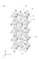
また、金属酸窒化物はペロブスカイト構造を有している。図2にペロブスカイト構造を示す。図2に示すように、ペロブスカイト構造においては、陰イオン(11,12)が6つの頂点を占め、中心にBサイト原子13が存在する八面体15が頂点を互いに共有して3次元ネットワークを構成しており、このネットワークの間隙にAサイト原子14が配置されている。Aサイト原子は、上述したように、バリウム、ストロンチウムおよびランタンからなる群から選ばれる少なくとも1つであり、Bサイト原子は、上述したように、タンタルおよびチタンからなる群から選ばれる少なくとも1つである。
Further, the metal oxynitride has a perovskite structure. FIG. 2 shows the perovskite structure. As shown in FIG. 2, in the perovskite structure, anions (11, 12) occupy six vertices, and an
本実施形態では、Aがペロブスカイト構造におけるAサイトを占めた場合に示すイオン価数をa、Bがペロブスカイト構造におけるBサイトを占めた場合に示すイオン価数をbとした場合、aおよびbが6.7≦a+b≦7.3である関係を満足する。 In the present embodiment, when the ionic valence indicated when A occupies the A site in the perovskite structure is a, and the ionic valence indicated when B occupies the B site in the perovskite structure is b, a and b are The relationship of 6.7 ≦ a + b ≦ 7.3 is satisfied.
なお、上記のイオン価数aとイオン価数bとは、それぞれ、平均価数として表される。平均価数は、Aサイト、または、Bサイトに存在するイオンの価数をその存在比に応じて平均化した値とする。例えば、AサイトにSrとLaが4:1のモル比で存在する場合について述べる。ペロブスカイト構造におけるSrイオンの価数は2であり、ペロブスカイト構造におけるLaイオンの価数は3である。よって、Aサイトの平均価数aは下記の(式1)により算出され、aは2.2価となる。
(式1)
(上記の場合の平均価数a)
=2(Srイオンの価数)×4/5(Srイオンの存在比)+3(Laイオンの価数)×1/5(Laイオンの存在比)
=8/5+3/5
=11/5
=2.2…(1)
The ionic valence a and the ionic valence b are expressed as average valences, respectively. The average valence is a value obtained by averaging the valences of ions existing at the A site or the B site according to their abundance ratio. For example, a case where Sr and La are present at the A site in a molar ratio of 4: 1 will be described. The valence of Sr ions in the perovskite structure is 2, and the valence of La ions in the perovskite structure is 3. Therefore, the average valence a of the A site is calculated by the following (Equation 1), and a is 2.2 valence.
(Equation 1)
(Average valence a in the above case)
= 2 (Sr ion valence) x 4/5 (Sr ion abundance ratio) + 3 (La ion valence) x 1/5 (La ion abundance ratio)
= 8/5 + 3/5
= 11/5
= 2.2 ... (1)
同様に、BサイトにTaとTiが4:1のモル比で存在する場合について述べる。ペロブスカイト構造におけるTaイオンの価数は5であり、ペロブスカイト構造におけるTiイオンの価数は4である。よって、Bサイトの平均価数bは下記の(式2)により算出され、bは4.8価となる。
(式2)
(上記の場合の平均価数b)
=5(Taイオンの価数)×4/5(Taイオンの存在比)+4(Tiイオンの価数)×1/5(Tiイオンの存在比)
=20/5+4/5
=24/5=4.8…(2)
Similarly, the case where Ta and Ti are present at the B site in a molar ratio of 4: 1 will be described. The valence of Ta ions in the perovskite structure is 5, and the valence of Ti ions in the perovskite structure is 4. Therefore, the average valence b of the B site is calculated by the following (Equation 2), and b has a 4.8 valence.
(Equation 2)
(Average valence b in the above case)
= 5 (Ta ion valence) x 4/5 (Ta ion abundance ratio) + 4 (Ti ion valence) x 1/5 (Ti ion abundance ratio)
= 20/5 + 4/5
= 24/5 = 4.8 ... (2)
上記の平均価数は、Aサイトに存在するイオンと、Bサイトに存在するイオンとのモル比が1:1である場合に算出される価数である。一方、平均価数は、Aサイトに存在するイオンと、Bサイトに存在するイオンとのモル比が1:1ではない場合に算出される価数であってもよい。 The above average valence is a valence calculated when the molar ratio of the ions present at the A site to the ions present at the B site is 1: 1. On the other hand, the average valence may be a valence calculated when the molar ratio of the ions present at the A site to the ions present at the B site is not 1: 1.
たとえば、Aサイトに存在するSrイオンと、Bサイトに存在するTaイオンとのモル比が、1:1.02である場合には、上記の式(1)および式(2)を用いて、aは2価、bは5.1価となる。
(平均価数a)
=2×1=2
(平均価数b)
=5×1.02=5.1
For example, when the molar ratio of the Sr ion present at the A site to the Ta ion present at the B site is 1: 1.02, the above formulas (1) and (2) are used. a is divalent and b is 5.1 valence.
(Average valence a)
= 2 × 1 = 2
(Average valence b)
= 5 x 1.02 = 5.1
上記のAサイトの平均価数aとBサイトの平均価数bとの和が上記の範囲を満足することにより、強誘電性を有しつつ、誘電損失が小さい金属酸窒化物薄膜を得ることが容易となる。 When the sum of the average valence a of the A site and the average valence b of the B site satisfies the above range, a metal oxynitride thin film having a ferroelectricity and a small dielectric loss can be obtained. Becomes easier.
一方、陰イオンは、金属酸窒化物ABOxNy中の酸素と窒素との組成比に応じて配分されており、ABOxNyにおいてx=2、y=1である場合、当該八面体はBO4N2八面体である。すなわち、図2に示すように、BO4N2八面体において、陰イオンが占める6つの頂点のうち、2つの頂点を窒素イオン12が占める。
On the other hand, anions, depending on the composition ratio of oxygen and nitrogen in the metal oxynitride of ABO x N y are allocated, if it is x = 2, y = 1 in the ABO x N y, the octahedral Is a BO 4 N 2 octahedron. That is, as shown in FIG. 2, in the BO 4 N 2 octahedron,
本実施形態では、金属酸窒化物は強誘電性を有している。強誘電性は、自発分極の向きが外部電界により反転し、外部電界を取り去っても分極が残る性質である。自発分極は、結晶中の陽イオンおよび陰イオンの位置が相対的に変化することにより生じる電荷分布の偏りである。 In this embodiment, the metal oxynitride has ferroelectricity. Ferroelectricity is a property in which the direction of spontaneous polarization is reversed by an external electric field, and polarization remains even when the external electric field is removed. Spontaneous polarization is a bias in the charge distribution caused by the relative changes in the positions of cations and anions in a crystal.
したがって、強誘電性を有する物質は、電荷分布の偏りが生じるような構造を有している。たとえば、ペロブスカイト型強誘電体として知られるチタン酸バリウム(BaTiO3)は、室温において、正方晶系の結晶構造を有しており、c軸方向の格子長さが、a軸方向およびb軸方向の格子長さよりも長い。したがって、単位格子において、酸素イオンの重心位置からチタンイオンの位置がずれている配置に起因して自発分極が生じている。このような配置は、中心対称性を有していない配置である。このような自発分極が生じているか否かは、たとえば、金属酸窒化物が圧電応答をするか否かにより評価することができる。 Therefore, the ferroelectric substance has a structure in which the charge distribution is biased. For example, barium titanate (BaTIO 3 ), known as a perovskite-type ferroelectric, has a tetragonal crystal structure at room temperature, and the lattice length in the c-axis direction is in the a-axis direction and the b-axis direction. Longer than the lattice length of. Therefore, in the unit cell, spontaneous polarization occurs due to the arrangement in which the position of the titanium ion is deviated from the position of the center of gravity of the oxygen ion. Such an arrangement is an arrangement that does not have central symmetry. Whether or not such spontaneous polarization occurs can be evaluated by, for example, whether or not the metal oxynitride has a piezoelectric response.
一方、外部電界を取り去ると分極がなくなる物質を常誘電体と呼ぶ。チタン酸バリウムは高温において立方晶系の結晶構造に転移して、c軸方向の格子長さが、a軸方向およびb軸方向の格子長さと同じとなる。その結果、チタン酸バリウムは強誘電性を失い、常誘電体となる。すなわち、酸素イオンの重心位置とチタンイオンの重心位置とが一致する配置となり、電荷分布の偏りが生じない構造に転移することにより、自発分極が消滅する。このような配置は、中心対称性を有する配置である。 On the other hand, a substance whose polarization disappears when the external electric field is removed is called a normal dielectric. Barium titanate transitions to a cubic crystal structure at high temperatures, and the lattice length in the c-axis direction becomes the same as the lattice length in the a-axis direction and the b-axis direction. As a result, barium titanate loses ferroelectricity and becomes a normal dielectric. That is, the position of the center of gravity of the oxygen ion and the position of the center of gravity of the titanium ion coincide with each other, and the spontaneous polarization disappears by shifting to a structure in which the charge distribution is not biased. Such an arrangement is an arrangement having central symmetry.
通常、強誘電性を有している物質は、中心対称性を有していない配置(非中心対称性を有する配置)が秩序を持って繰り返される領域のみを有している。しかしながら、本実施形態では、上記の金属酸窒化物は、中心対称性を示す回折を生じる領域と、非中心対称性を示す回折を生じる領域とを有しており、非中心対称性を示す回折を生じる領域に起因する強誘電性を示すことができる。 Generally, a substance having ferroelectricity has only a region in which an arrangement having no central symmetry (an arrangement having non-central symmetry) is repeated in an orderly manner. However, in the present embodiment, the above-mentioned metal oxynitride has a region that causes diffraction that exhibits central symmetry and a region that produces diffraction that exhibits non-centrosymmetry, and diffraction that exhibits non-centrosymmetry. It is possible to show the ferroelectricity due to the region where the above occurs.
本実施形態では、中心対称性を示す回折を生じる領域と、非中心対称性を示す回折を生じる領域と、は、どちらも非中心対称性を有する配置から構成されている。しかしながら、中心対称性を示す回折を生じる領域と、非中心対称性を有する回折を生じる領域と、においては、陰イオン(酸素イオンおよび窒素イオン)の配置秩序が維持される範囲が異なる。 In the present embodiment, the region that produces diffraction that exhibits central symmetry and the region that produces diffraction that exhibits non-central symmetry are both configured with an arrangement that has non-central symmetry. However, the range in which the arrangement order of anions (oxygen ions and nitrogen ions) is maintained differs between the region where diffraction showing central symmetry and the region where diffraction having non-center symmetry occurs.
中心対称性を示す回折を生じる領域では、陰イオンの配置は非中心対称性を有する配置となっているものの、その配置が結晶粒子全体にランダムに存在しており、また非中心対称性を有する配置は単位格子の大きさ程度であり、非中心対称性に起因して生じる分極が影響を与える範囲が小さい。したがって、当該領域では、分極の向きが全方位的に存在しているので、当該領域は全体として特定の方向に向いた分極は存在せず、中心対称性を有していると見なすことができる。その結果、本実施形態に係る金属酸窒化物を回折法により分析すると、当該領域は、中心対称性を示す回折が生じる領域であり、第2相としての非中心対称性を示す回折を生じる領域としては検出されない。 In the region where diffraction showing central symmetry occurs, the arrangement of anions has non-central symmetry, but the arrangement is randomly present throughout the crystal particles and has non-central symmetry. The arrangement is about the size of a unit cell, and the range affected by polarization caused by non-central symmetry is small. Therefore, since the direction of polarization exists in all directions in the region, it can be considered that the region as a whole has no polarization directed in a specific direction and has central symmetry. .. As a result, when the metal oxynitride according to the present embodiment is analyzed by a diffraction method, the region is a region where diffraction showing central symmetry occurs, and a region where diffraction showing non-central symmetry as the second phase occurs. Is not detected as.
一方、非中心対称性を有する配置が秩序的に配列している領域では、特定の方向に配置秩序が繰り返されるため、その方向において非中心対称性が強められる。このような領域がある程度の大きさになると、この領域において生じる回折が、中心対称性を示す回折に影響を与えることがある。後述するが、非中心対称性を示す回折が生じると、中心対称性を示す回折が影響され、中心対称性を示す回折が生じる領域のみから構成される金属酸窒化物が示す回折パターンとは異なる回折パターンが得られる。 On the other hand, in the region where the arrangements having non-central symmetry are arranged in an orderly manner, the arrangement order is repeated in a specific direction, so that the non-central symmetry is strengthened in that direction. When such a region becomes a certain size, the diffraction generated in this region may affect the diffraction showing central symmetry. As will be described later, when diffraction showing non-central symmetry occurs, the diffraction showing central symmetry is affected, which is different from the diffraction pattern shown by metal oxynitride, which is composed of only the region where diffraction showing central symmetry occurs. A diffraction pattern is obtained.
このような回折パターンが得られる金属酸窒化物では、陰イオンが秩序的に配列している領域が大きく、強誘電性を発現させる起点となる。一方、金属酸窒化物が中心対称性を示す回折が生じる領域を有することにより、誘電損失が小さくなる。 In the metal oxynitride from which such a diffraction pattern can be obtained, a region in which anions are arranged in an orderly manner is large, which is a starting point for exhibiting ferroelectricity. On the other hand, since the metal oxynitride has a region where diffraction showing central symmetry occurs, the dielectric loss becomes small.
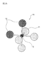
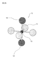
BO4N2八面体では、図3Aに示すように、2個の窒素(N)イオン12が互いに隣り合う配置(cis配置)と、図3Bに示すように、2個の窒素イオン(N)12が互いに隣り合わない配置(trans配置)と、がある。酸素イオンの結合長さと窒素イオンの結合長さとが異なるので、cis配置およびtrans配置のどちらも非中心対称性を有する配置である。
In the BO 4 N 2 octahedron, two nitrogen (N)
本実施形態では、非中心対称性を有する配置は、cis配置であることが好ましい。したがって、中心対称性を示す回折を生じる領域および非中心対称性を示す回折を生じる領域は、cis配置から構成されていることが好ましい。 In the present embodiment, the arrangement having non-central symmetry is preferably the cis arrangement. Therefore, it is preferable that the region showing diffraction at the center symmetry and the region causing diffraction showing non-center symmetry are composed of a cis arrangement.
図3Aに示すcis配置のBO4N2八面体では、a軸方向とc軸方向とに窒素イオンが存在しているが、a軸方向とb軸方向とに窒素イオンが存在するBO4N2八面体およびb軸方向とc軸方向とに窒素イオンが存在するBO4N2八面体もcis配置である。したがって、これらのBO4N2八面体がランダムに存在し、頂点共有することにより、非中心対称性が弱められ、中心対称性を示す回折を生じる領域が形成される。 The BO 4 N 2 octahedra cis configuration shown in FIG. 3A, although the nitrogen ions are present in the a-axis direction and the c-axis direction, there is nitrogen ions in the a-axis direction and the b-axis direction BO 4 N The 2 octahedron and the BO 4 N 2 octahedron in which nitrogen ions are present in the b-axis direction and the c-axis direction are also in the cis arrangement. Therefore, these BO 4 N 2 octahedrons randomly exist, and by sharing the vertices, the non-central symmetry is weakened, and a region showing diffraction showing the central symmetry is formed.
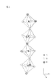
これに対して、cis配置が秩序を持って存在する構造を図4に示す。図4において、cis配置秩序構造では、八面体の頂点のうち、c軸方向のサイト(4a)の1つと、a軸およびb軸に平行な面上のサイト(8h)の1つと、に窒素が配置されている。その結果、BO4N2八面体は、Bを結ぶ軸(図3ではc軸)から傾いた状態で連なった八面体鎖を形成する。本実施形態では、窒素がcis配置である八面体が連なって形成されるこのような秩序構造が、BO4N2八面体がランダムに存在にする(BO4N2八面体の秩序範囲が狭い)領域に起因する回折パターンに影響を与える。 On the other hand, FIG. 4 shows a structure in which the cis arrangement exists in an orderly manner. In FIG. 4, in the cis-arranged ordered structure, among the vertices of the octahedron, one of the sites in the c-axis direction (4a) and one of the sites on the plane parallel to the a-axis and the b-axis (8h) are nitrogen. Is placed. As a result, the BO 4 N 2 octahedron forms an octahedral chain that is tilted from the axis connecting B (the c axis in FIG. 3). In the present embodiment, such an ordered structure in which octahedrons in which nitrogen is cis-arranged is formed so that BO 4 N 2 octahedrons are randomly present ( the order range of BO 4 N 2 octahedrons is narrow). ) Affects the diffraction pattern due to the region.
なお、中心対称性を示す回折を生じる領域と、非中心対称性を示す回折を生じる領域と、において、陽イオンの種類が同じであってもよいし、異なっていてもよい。本実施形態では、陽イオンの種類は同じであることが好ましい。金属酸窒化物を構成する元素の種類を少なくすることにより、コンタミが抑制でき、製造プロセスの負荷を低減することができる。 It should be noted that the type of cation may be the same or different in the region where the diffraction showing the central symmetry is generated and the region where the diffraction showing the non-central symmetry is generated. In this embodiment, it is preferable that the types of cations are the same. By reducing the types of elements that make up the metal oxynitride, contamination can be suppressed and the load on the manufacturing process can be reduced.
金属酸窒化物において、中心対称性を示す回折を生じる領域と非中心対称性を示す回折を生じる領域とが存在しているか否かは、たとえば、以下のようにして評価することができる。このような原子の位置により決定される構造は、XRD回折により評価することが多い。しかしながら、上述したように、上記の金属酸窒化物において、中心対称性を示す回折を生じる領域であるか、非中心対称性を示す回折を生じる領域であるかは、陰イオン(酸素および窒素)の配置の違いに依存している。酸素および窒素のような軽元素の位置を反映する回折ピークの強度は、金属元素(AおよびB)の位置を反映する回折ピークの強度よりも弱く、軽元素の位置を反映する回折ピークを直接評価することは困難である。 In the metal oxynitride, whether or not there is a region showing diffraction showing central symmetry and a region causing diffraction showing non-central symmetry can be evaluated, for example, as follows. The structure determined by the position of such an atom is often evaluated by XRD diffraction. However, as described above, in the above-mentioned metal oxynitride, whether it is a region showing diffraction showing central symmetry or a region showing diffraction showing non-central symmetry is determined by anions (oxygen and nitrogen). It depends on the difference in the arrangement of. The intensity of the diffraction peak reflecting the position of light elements such as oxygen and nitrogen is weaker than the intensity of the diffraction peak reflecting the position of the metal elements (A and B), and the diffraction peak reflecting the position of the light element is directly applied. It is difficult to evaluate.
しかしながら、陰イオンの配置の違いは、XRD回折により観察される回折ピークの強度に影響を与えることがある。そこで、本実施形態では、所定の面で反射される回折ピークの強度と、別の面で反射される回折ピークの強度との比に基づき、金属酸窒化物中に、中心対称性を示す回折を生じる領域と非中心対称性を示す回折を生じる領域とが存在しているか否かを評価する。 However, the difference in the arrangement of anions may affect the intensity of the diffraction peak observed by XRD diffraction. Therefore, in the present embodiment, diffraction showing central symmetry in the metal oxynitride is based on the ratio of the intensity of the diffraction peak reflected on a predetermined surface to the intensity of the diffraction peak reflected on another surface. It is evaluated whether or not there is a region where the above occurs and a region where the diffraction showing non-central symmetry exists.
まず、中心対称性を示す回折を生じる領域のみから構成されるペロブスカイト型金属酸窒化物に対する粉末XRD回折の測定結果またはシミュレーション結果を得る。X線源がCu−Kα線である場合、回折角2θが20°から25°の範囲内に現れる回折ピークのうち、最強の回折ピークP1の強度と、回折角2θが44°から50°の範囲内に現れる回折ピークのうち、最強の回折ピークP2の強度と、から強度比IRr(P1の強度/P2の強度)を算出し、リファレンスとする。XRD回折シミュレーションは公知のソフトウェアで行うことができる。 First, a measurement result or a simulation result of powder XRD diffraction for a perovskite type metal oxynitride composed of only a region showing diffraction showing central symmetry is obtained. When the X-ray source is Cu-Kα ray, the intensity of the strongest diffraction peak P1 and the diffraction angle 2θ of 44 ° to 50 ° among the diffraction peaks appearing in the diffraction angle 2θ within the range of 20 ° to 25 °. Among the diffraction peaks appearing in the range, the intensity of the strongest diffraction peak P2 and the intensity ratio IR r (intensity of P1 / intensity of P2) are calculated and used as a reference. The XRD diffraction simulation can be performed with known software.
次に、リファレンスと同じ組成を有する金属酸窒化物に対して、XRD回折測定を行い、回折ピークのパターンを得る。得られた回折ピークのパターンにおいて、回折ピークP1の強度と、回折ピークP2の強度と、から強度比IR(P1の強度/P2の強度)を算出して、リファレンスの強度比を100%としたときの比率A(IR/IRr)を算出することにより、金属酸窒化物中において中心対称性を示す回折を生じる領域と非中心対称性を示す回折を生じる領域とが存在しているか否かを評価することができる。 Next, XRD diffraction measurement is performed on the metal oxynitride having the same composition as the reference to obtain a pattern of diffraction peaks. In the obtained diffraction peak pattern, the intensity ratio IR (intensity of P1 / intensity of P2) was calculated from the intensity of the diffraction peak P1 and the intensity of the diffraction peak P2, and the intensity ratio of the reference was set to 100%. By calculating the ratio A (IR / IR r ), whether or not there is a region in the metal oxynitride that causes diffraction that shows central symmetry and a region that causes diffraction that shows non-central symmetry. Can be evaluated.
なお、回折ピークの強度比は配向によっても変化するが、上記の強度比IRは配向に起因していないため、強度比IR(P1の強度/P2の強度)は面直(out of plane)方向、面内(in-plane)方向の両方から測定された回折ピークにおいて同じ関係を示す。例えば、P1の強度/P2の強度<1が維持される。一方、配向している場合は、面直方向、面内方向でその関係が逆転する。例えば、面直方向ではP1の強度/P2の強度>1であるのに対し、面内方向ではP1の強度/P2の強度<1となる。 The intensity ratio of the diffraction peak also changes depending on the orientation, but since the above-mentioned intensity ratio IR is not caused by the orientation, the intensity ratio IR (intensity of P1 / intensity of P2) is in the out of plane direction. , The same relationship is shown for diffraction peaks measured from both in-plane directions. For example, the strength of P1 / the strength of P2 <1 is maintained. On the other hand, when they are oriented, the relationship is reversed in the perpendicular direction and the in-plane direction. For example, the strength of P1 / the strength of P2> 1 in the perpendicular direction, whereas the strength of P1 / the strength of P2 <1 in the in-plane direction.
本実施形態では、比率Aが0%以上80%以下である時に、金属酸窒化物中に、中心対称性を示す回折を生じる領域と、非中心対称性を示す回折を生じる領域とが存在していると判断する。 In the present embodiment, when the ratio A is 0% or more and 80% or less, there is a region in the metal oxynitride that causes diffraction that shows central symmetry and a region that causes diffraction that shows non-central symmetry. Judge that
なお、本実施形態に係る金属酸窒化物薄膜は無配向であることが好ましい。本実施形態では、無配向であるか否かは以下のようにして判断する。まず、金属酸窒化物結晶において直交する2つの面を選択する。金属酸窒化物薄膜について、in-plane,out-of-plane方向の両方からXRD測定を行い、in-plane方向のXRD測定において強度が大きかった方のピークを基準とし、基準のピーク強度100%に対して小さい方のピーク強度の割合B1(小さい方なので<100%)を算出しておく。続いて、out-of-plane方向のXRD測定においてin-plane方向のXRD測定で基準とした位置のピークの強度100%に対して他方のピーク強度の割合B2を算出する。そして、この両者の差(|B1−B2|)が80%以内である場合に、薄膜が無配向であると判断する。 The metal oxynitride thin film according to this embodiment is preferably non-oriented. In the present embodiment, it is determined as follows whether or not it is non-oriented. First, two orthogonal planes are selected in the metal oxynitride crystal. For the metal oxynitride thin film, XRD measurement is performed from both the in-plane and out-of-plane directions, and the peak with the higher intensity in the XRD measurement in the in-plane direction is used as a reference, and the standard peak intensity is 100%. The ratio of the smaller peak intensity to B1 (<100% because it is the smaller one) is calculated. Subsequently, in the out-of-plane direction XRD measurement, the ratio B2 of the other peak intensity to 100% of the peak intensity at the position used as the reference in the in-plane direction XRD measurement is calculated. Then, when the difference between the two (| B1-B2 |) is within 80%, it is determined that the thin film is non-oriented.
具体的な例を示すと、in-plane方向のXRD測定において、(220)面のピーク強度100%に対して、(002)面のピーク強度が80%であるところ、out-of-plane方向のXRD測定において、(220)面のピーク強度100%に対して、(002)面のピーク強度が120%である場合、(002)面のピーク強度の差は、40%(120%−80%)となる。したがって、この場合には、金属酸窒化物薄膜は無配向であると判断される。 To show a specific example, in the XRD measurement in the in-plane direction, where the peak intensity of the (002) plane is 80% with respect to the peak intensity of the (220) plane, it is in the out-of-plane direction. In the XRD measurement of (220), when the peak intensity of the (002) plane is 120% with respect to the peak intensity of the (220) plane, the difference in the peak intensity of the (002) plane is 40% (120% -80). %). Therefore, in this case, it is determined that the metal oxynitride thin film is non-oriented.
また、中性子線回折を利用すれば、軽元素の位置を評価することができる。中性子線回折測定結果により精密化させた結晶構造において、ABO2NがSrTaO2Nまたは(SrLa)TaO2Nである場合には、中心対称性を有する構造は空間群I4/mcm(Table No.140)に属し、cis配置秩序構造に起因する非中心対称性を有する構造は空間群Pmc21(Table No.26)に属することが知られている。 Moreover, the position of a light element can be evaluated by using neutron diffraction. In the crystal structure refined by the neutron radiation diffraction measurement result, when ABO 2 N is SrTaO 2 N or (SrLa) TaO 2 N, the structure having centrosymmetry is the space group I4 / mcm (Table No. It is known that the structure belonging to 140) and having non-centrosymmetry due to the cis arrangement ordered structure belongs to the space group Pmc2 1 (Table No. 26).
ABO2NがBaTaO2Nまたは(BaLa)TaO2Nである場合には、中心対称性を有する構造は空間群Pm−3m(Table No.221)に属し、cis配置秩序構造に起因する非中心対称性を有する構造は空間群Pmc21(Table No.26)に属していることが知られている。 When ABO 2 N is BaTaO 2 N or (BaLa) TaO 2 N, the structure having central symmetry belongs to the space group Pm-3m (Table No.221) and is non-centered due to the cis arrangement ordered structure. It is known that the symmetric structure belongs to the space group Pmc2 1 (Table No. 26).
(2.薄膜キャパシタの製造方法)
次に、図1に示す薄膜キャパシタ1の製造方法の一例について以下に説明する。
(2. Manufacturing method of thin film capacitor)
Next, an example of the method for manufacturing the thin film capacitor 1 shown in FIG. 1 will be described below.
まず、基板51を準備する。基板51として、たとえば、Si単結晶基板を用いる場合、当該基板の一方の主面に絶縁層(たとえば、SiO2)を形成する。絶縁層を形成する方法としては、熱酸化法、CVD(Chemical Vapor Deposition)法等の公知の成膜法を用いればよい。
First, the
続いて、形成された絶縁層上に、公知の成膜法、たとえば、スパッタリング法を用いて第1の電極を構成する材料の薄膜を形成して第1の電極52を形成する。
Subsequently, a thin film of the material constituting the first electrode is formed on the formed insulating layer by using a known film forming method, for example, a sputtering method, to form the
続いて、公知の成膜法を用いて、金属酸窒化物薄膜53を第1の電極52上に形成する。
Subsequently, a metal oxynitride
公知の成膜法としては、たとえば、真空蒸着法、スパッタリング法、パルスレーザー蒸着法(Pulsed Laser Deposition:PLD)、有機金属化学気相成長法(Metal-Organic Chemical Vapor Deposition:MOCVD)、有機金属分解法(Metal Organic Decomposition:MOD)またはゾルゲル法、化学溶液堆積法(Chemical Solution Deposition:CSD)が例示される。 Known film forming methods include, for example, vacuum vapor deposition, sputtering, pulsed laser deposition (PLD), metal-organic chemical vapor deposition (MOCVD), and organic metal decomposition. Examples include the method (Metal Organic Decomposition: MOD), the sol-gel method, and the chemical solution deposition method (CSD).
成膜用原料としては、たとえば、各種ターゲット材料、蒸着材料、有機金属材料等が例示される。成膜用原料には微量の不純物、副成分が含まれている場合があるが、本発明の効果を大きく劣化させるものでなければ、特に問題はない。 Examples of the raw material for film formation include various target materials, vapor deposition materials, organic metal materials, and the like. The raw material for film formation may contain trace amounts of impurities and subcomponents, but there is no particular problem as long as the effects of the present invention are not significantly deteriorated.
これらの成膜法のうち、成膜用原料を一旦原子レベルまたは分子レベルに分離または励起した後に、基板上に堆積させて成膜を行う公知の気相成長法が好ましい。以下では、気相成長法として、スパッタリング法を用いて、金属酸窒化物薄膜を成膜する方法について述べる。 Among these film forming methods, a known vapor deposition method in which a film-forming raw material is once separated or excited at the atomic level or the molecular level and then deposited on a substrate to form a film is preferable. Hereinafter, a method of forming a metal oxynitride thin film by using a sputtering method as a vapor phase growth method will be described.
スパッタリング法を用いて金属酸窒化物薄膜を成膜する場合、成膜用原料として、所定の組成を有するターゲットを用いる。また、Aサイト原子であるバリウムおよび/またはストロンチウムの一部をランタンで置換すると、ペロブスカイト構造が歪みやすい。したがって、Aサイト原子として、ランタンを所定の割合で含むターゲットを用いることにより、結晶構造の一部において、対称性を低下させ、中心対称性を示す回折を生じる領域中に、非中心対称性を示す回折を生じる領域を形成することが容易となる。 When a metal oxynitride thin film is formed by a sputtering method, a target having a predetermined composition is used as a raw material for the film formation. Further, when a part of barium and / or strontium, which are A-site atoms, is replaced with lantern, the perovskite structure is easily distorted. Therefore, by using a target containing a lantern in a predetermined ratio as the A-site atom, the non-central symmetry is reduced in a part of the crystal structure and the non-central symmetry is generated in the region where the diffraction showing the central symmetry is generated. It becomes easy to form the region where the indicated diffraction occurs.
成膜時には、薄膜を結晶化させるために、基板を加熱することが好ましい。成膜時の基板温度は、薄膜の構成元素、組成等に応じて決定すればよいが、本実施形態では、強度比を上記の範囲内とするために、基板温度は500℃〜800℃の範囲内であることが好ましい。基板温度が低すぎると、薄膜が結晶化しない傾向にあり、基板温度が高すぎると、窒素が脱離する傾向にある。 At the time of film formation, it is preferable to heat the substrate in order to crystallize the thin film. The substrate temperature at the time of film formation may be determined according to the constituent elements, composition, etc. of the thin film, but in the present embodiment, the substrate temperature is 500 ° C. to 800 ° C. in order to keep the strength ratio within the above range. It is preferably within the range. If the substrate temperature is too low, the thin film tends not to crystallize, and if the substrate temperature is too high, nitrogen tends to be desorbed.
また、強度比を上記の範囲内とするために、高周波電力(印加電力)は50W〜300Wの範囲内であることが好ましい。高周波電力が小さすぎると、成膜レートが顕著に低下する傾向がある。一方、高周波電力が大きすぎると、異常粒成長により特性が低下する傾向がある。 Further, in order to keep the intensity ratio within the above range, the high frequency power (applied power) is preferably in the range of 50 W to 300 W. If the high frequency power is too small, the film formation rate tends to decrease significantly. On the other hand, if the high frequency power is too large, the characteristics tend to deteriorate due to abnormal grain growth.
ターゲットとして、酸化物を用いる場合、成膜時の雰囲気ガスは、酸素ガスおよび窒素ガスを少なくとも含む。このような雰囲気ガスを用いることにより、得られる薄膜の絶縁特性が確保され、誘電体としての薄膜が得られる。本実施形態では、強度比を上記の範囲内とするために、酸素ガス圧は0.01Pa以上0.1Pa以下の範囲内であることが好ましい。酸素ガス圧を上記の範囲内とすることにより、結晶中において対称性の低下が生じやすくなり、強度比を上記の範囲内とすることが容易となる。同様に、窒素ガス圧は0.01Pa以上0.1Pa以下の範囲内であることが好ましい。 When an oxide is used as the target, the atmospheric gas at the time of film formation contains at least oxygen gas and nitrogen gas. By using such an atmospheric gas, the insulating characteristics of the obtained thin film are ensured, and a thin film as a dielectric can be obtained. In the present embodiment, the oxygen gas pressure is preferably in the range of 0.01 Pa or more and 0.1 Pa or less in order to keep the intensity ratio within the above range. By setting the oxygen gas pressure within the above range, the symmetry tends to be lowered in the crystal, and the intensity ratio can be easily set within the above range. Similarly, the nitrogen gas pressure is preferably in the range of 0.01 Pa or more and 0.1 Pa or less.
また、雰囲気ガスと別にArガス等の不活性ガスを導入すると良い。Arガスはターゲットから原子をたたき出すのに使用されるため、プラズマが安定に維持される圧力を得るために必要な量を導入すると良い。なお、プラズマが安定に維持される状態は入力電圧とArガス圧に依存するため、チャンバーの大きさおよびターゲットのサイズに合わせてそれらを調整すればよい。 Further, it is advisable to introduce an inert gas such as Ar gas separately from the atmospheric gas. Since Ar gas is used to knock atoms out of the target, it is advisable to introduce the amount required to obtain a pressure that keeps the plasma stable. Since the state in which the plasma is stably maintained depends on the input voltage and the Ar gas pressure, they may be adjusted according to the size of the chamber and the size of the target.
また、本実施形態では、成膜時に、金属酸化物薄膜を経由せず、金属酸窒化物を基板上に直接成膜してもよいし、金属酸化物薄膜を成膜し、成膜した金属酸化物薄膜の結晶構造内に窒素を導入して金属酸窒化物薄膜を得てもよい。どちらの場合であっても、窒化処理として、金属酸化物膜の成膜時に窒素ラジカルを成膜室に導入する方法、窒素ガスなどを用いる反応性スパッタを用いる方法、プラズマ窒化により活性化された窒素を用いる方法等を用いることが可能である。 Further, in the present embodiment, the metal oxynitride may be directly formed on the substrate without passing through the metal oxide thin film at the time of film formation, or the metal formed by forming the metal oxide thin film. Nitrogen may be introduced into the crystal structure of the oxide thin film to obtain a metal oxynitride thin film. In either case, as the nitriding treatment, a method of introducing nitrogen radicals into the film forming chamber at the time of film formation of the metal oxide film, a method of using reactive sputtering using nitrogen gas or the like, or a method of activating by plasma nitriding. It is possible to use a method using nitrogen or the like.
このような方法によれば、毒性のある気体を使用せずに金属酸窒化物薄膜を成膜できるので、好ましい。また、金属窒化物薄膜の部分酸化処理なども用いることが可能である。本実施形態では、金属酸化物の原料を用いて成膜する際に、窒化に用いる窒素を導入して、金属酸窒化物を得ることが好ましい。 Such a method is preferable because a metal oxynitride thin film can be formed without using a toxic gas. It is also possible to use a partial oxidation treatment of the metal nitride thin film. In the present embodiment, it is preferable to introduce nitrogen used for nitriding to obtain a metal oxynitride when forming a film using a metal oxide raw material.
このようにして得られる金属酸窒化物薄膜は、誘電体として働く堆積膜である。 The metallic oxynitride thin film thus obtained is a deposited film that acts as a dielectric.
次に、本実施形態では、形成した金属酸窒化物薄膜53上に、公知の成膜法を用いて上部電極を構成する材料の薄膜を形成して第2の電極54を形成する。
Next, in the present embodiment, a thin film of the material constituting the upper electrode is formed on the formed metal oxynitride
以上の工程を経て、図1に示すように、基板51上に、キャパシタ部(第2の電極52、金属酸窒化物薄膜53および第2の電極54)が形成された薄膜キャパシタ1が得られる。
Through the above steps, as shown in FIG. 1, a thin film capacitor 1 in which a capacitor portion (
(3.本実施形態のまとめ)
本実施形態では、金属酸窒化物は、中心対称性を示す回折を生じる領域と非中心対称性を示す回折を生じる領域とを有している。中心対称性を示す回折を生じる領域は、非中心対称性を有する配置から構成されており、微視的に見ると、非中心対称性に起因する自発分極が生じているものの、非中心対称性を有する配置はランダムな方向に存在しているので、生じる自発分極は打ち消される。その結果、非中心対称性を有する配置から構成されているにもかかわらず、中心対称性を示す回折が生じる。したがって、当該領域全体では自発分極は生じないので、当該領域は常誘電性である。
(3. Summary of this embodiment)
In the present embodiment, the metal oxynitride has a region that causes diffraction that exhibits central symmetry and a region that produces diffraction that exhibits non-central symmetry. The region that causes diffraction that shows central symmetry is composed of an arrangement that has non-central symmetry, and when viewed microscopically, although spontaneous polarization due to non-central symmetry occurs, non-central symmetry Since the arrangements with are present in random directions, the spontaneous polarization that occurs is canceled out. As a result, diffraction that exhibits central symmetry occurs, even though it is composed of arrangements that have non-central symmetry. Therefore, since spontaneous polarization does not occur in the entire region, the region is isoelectric.
一方、非中心対称性を有する配置が秩序を持っている存在している領域が、自発分極が生じる程度に大きいので、当該領域では、結合長さが異なる2種の陰イオンの変位により自発分極が生じている。したがって、当該領域は強誘電性である。 On the other hand, since the region where the arrangement having non-central symmetry is ordered is large enough to cause spontaneous polarization, in this region, spontaneous polarization is caused by the displacement of two types of anions having different bond lengths. Is occurring. Therefore, the region is ferroelectric.
その結果、中心対称性を示す回折を生じる領域と非中心対称性を示す回折を生じる領域との両方が存在していることにより、金属酸窒化物は、全体として強誘電性を示しつつ、誘電損失が小さい。したがって、強誘電性を利用する用途に好適でありながら、常誘電体の特徴である誘電損失の小ささを兼ね備えることができる。 As a result, the metal oxynitride is dielectric while exhibiting ferroelectricity as a whole due to the existence of both a region showing diffraction showing central symmetry and a region causing diffraction showing non-central symmetry. The loss is small. Therefore, while being suitable for applications that utilize ferroelectricity, it can also have a small dielectric loss, which is a characteristic of ordinary dielectrics.
また、非中心対称性に起因する分極は2種の陰イオンの変位により実現されているので、結晶の歪みが、陽イオンの変位により生じる歪みよりも小さい。したがって、強誘電性と誘電損失とを両立することが容易である。 Further, since the polarization due to the non-central symmetry is realized by the displacement of the two types of anions, the strain of the crystal is smaller than the strain caused by the displacement of the cations. Therefore, it is easy to achieve both ferroelectricity and dielectric loss.
以上、本発明の実施形態について説明してきたが、本発明は上記の実施形態に何ら限定されるものではなく、本発明の範囲内において種々の態様で改変しても良い。 Although the embodiments of the present invention have been described above, the present invention is not limited to the above embodiments, and may be modified in various ways within the scope of the present invention.
以下、実施例において、本発明をさらに詳細に説明する。ただし、本発明は以下の実施例に限定されるものではない。 Hereinafter, the present invention will be described in more detail in Examples. However, the present invention is not limited to the following examples.
(実験1)
まず、成膜用原料としてのターゲットの原料として、炭酸ストロンチウム(SrCO3)、炭酸バリウム(BaCO3)、酸化ランタン(La2O3)、酸化チタン(TiO2)および酸化タンタル(Ta2O5)を準備した。準備した原料を、表1に示す組成(実施例1〜14および比較例1〜5)になるように秤量した。秤量後の原料を、溶媒としてのエタノールとともに湿式ボールミルにて16時間混合を行った。得られた混合スラリーを恒温乾燥機にて80℃で12時間乾燥した。得られた混合物を乳鉢にて軽く解砕し、セラミック製のるつぼにいれ電気炉で1000℃、大気雰囲気中で2時間熱処理し、仮焼物を得た。
(Experiment 1)
First, as target raw materials as raw materials for film formation, strontium carbonate (SrCO 3 ), barium carbonate (BaCO 3 ), lanthanum oxide (La 2 O 3 ), titanium oxide (TIO 2 ) and tantalum oxide (Ta 2 O 5) ) Was prepared. The prepared raw materials were weighed so as to have the compositions shown in Table 1 (Examples 1 to 14 and Comparative Examples 1 to 5). The weighed raw material was mixed with ethanol as a solvent in a wet ball mill for 16 hours. The obtained mixed slurry was dried at 80 ° C. for 12 hours in a constant temperature dryer. The obtained mixture was lightly crushed in a mortar, placed in a ceramic crucible, and heat-treated in an electric furnace at 1000 ° C. for 2 hours in an air atmosphere to obtain a calcined product.
得られた仮焼物を、溶媒としてのエタノールとともに湿式ボールミルにて16時間粉砕を行い、粉砕後スラリーを恒温乾燥機にて80℃で12時間乾燥し粉砕物を得た。得られた粉砕物に対し、バインダーとしてポリビニールアルコール溶液を溶液中の固形物換算で0.6重量%添加、混合し造粒物を得た。造粒物を直径約23mm、高さ約9mmの円柱形状に成形し成形物を得た。成形物を電気炉にて、大気雰囲気中1400℃で2時間焼成し、焼結体を得た。得られた焼結体の上面および下面を鏡面研磨し、焼結体の高さを5mmとした成膜用ターゲットを得た。 The obtained calcined product was pulverized with ethanol as a solvent in a wet ball mill for 16 hours, and after pulverization, the slurry was dried at 80 ° C. for 12 hours in a constant temperature dryer to obtain a pulverized product. To the obtained pulverized product, a polyvinyl alcohol solution as a binder was added in an amount of 0.6% by weight in terms of solid matter in the solution and mixed to obtain a granulated product. The granulated product was molded into a cylindrical shape having a diameter of about 23 mm and a height of about 9 mm to obtain a molded product. The molded product was fired in an electric furnace at 1400 ° C. for 2 hours in an air atmosphere to obtain a sintered body. The upper surface and the lower surface of the obtained sintered body were mirror-polished to obtain a film-forming target having a height of the sintered body of 5 mm.
上記のように得られた成膜用ターゲットを成膜装置に設置し、続いて、ターゲットに対向するよう表面に第1の電極としてPt膜を有するSi基板を設置した。窒素ラジカルを導入したスパッタリング法で厚さ500nmとなるように金属酸窒化物薄膜を成膜した。雰囲気ガスはAr、N2、O2を用いた。 The film-forming target obtained as described above was installed in the film-forming apparatus, and then a Si substrate having a Pt film as a first electrode on the surface was installed so as to face the target. A metal oxynitride thin film was formed so as to have a thickness of 500 nm by a sputtering method in which nitrogen radicals were introduced. Ar, N 2 , and O 2 were used as the atmospheric gas.
成膜条件は、基板温度を600℃、酸素ガス圧および窒素ガス圧を0.01Pa、プラズマ印加電力を150Wとし、実施例1〜14および比較例2〜5については、Arにより調整した全圧を2Pa以上とし、比較例1については、Arにより調整した全圧を1Pa以下とした。 The film forming conditions were a substrate temperature of 600 ° C., an oxygen gas pressure and a nitrogen gas pressure of 0.01 Pa, a plasma applied power of 150 W, and the total pressure adjusted by Ar for Examples 1 to 14 and Comparative Examples 2 to 5. Was 2 Pa or more, and in Comparative Example 1, the total pressure adjusted by Ar was 1 Pa or less.
次に、バルクの試料を以下のようにして作製した。まず、原料粉末として、炭酸ストロンチウム(SrCO3)粉末および酸化タンタル(Ta2O5)粉末を準備した。準備した粉末を、組成式SrTaO2Nで表される金属酸窒化物が得られるように秤量した。 Next, a bulk sample was prepared as follows. First, strontium carbonate (SrCO 3 ) powder and tantalum oxide (Ta 2 O 5 ) powder were prepared as raw material powders. The prepared powders were weighed so that the metal oxynitride represented by the composition formula SrTaO 2 N is obtained.
秤量したSrCO3粉末およびTa2O5粉末をエタノールで湿式混合し、1200℃−10時間の条件で仮焼きを空気中で2回行い、固相反応により、SrおよびTaを有する酸化物前駆体を得た。 Weighed SrCO 3 powder and Ta 2 O 5 powder are wet-mixed with ethanol, and calcined twice in air under the condition of 1200 ° C. for 10 hours. Oxide precursor having Sr and Ta is subjected to solid phase reaction. Got
続いて、得られた酸化物の前駆体に対して窒化処理を2回行い、組成式SrTaO2Nで表される金属酸窒化物粉末を得た。窒化処理では、NH3の供給速度を100ml/minとし、加熱温度を1000℃とし、加熱時間を20時間とした。 Then, it performs nitriding treatment twice for precursors of the obtained oxide, to obtain a metal oxynitride powder represented by a composition formula SrTaO 2 N. In the nitriding treatment, the supply rate of NH 3 was set to 100 ml / min, the heating temperature was set to 1000 ° C, and the heating time was set to 20 hours.
得られた金属酸窒化物粉末をボールミルにより16時間湿式粉砕した乾燥させた。乾燥後の金属酸窒化物粉末100質量%に対して、バインダーとしてポリビニールアルコールを0.6質量%添加して造粒し、造粒粉を得た。得られた造粒粉を金型に投入してプレス成形を行い、成形体を得た。 The obtained metallic oxynitride powder was wet-ground and dried by a ball mill for 16 hours. To 100% by mass of the metal oxynitride powder after drying, 0.6% by mass of polyvinyl alcohol was added as a binder for granulation to obtain a granulated powder. The obtained granulated powder was put into a mold and press-molded to obtain a molded product.
得られた成形体をN2雰囲気下で焼成し、バルクの金属酸窒化物焼成体を得た。焼成条件は、保持温度を1400℃とし、保持時間を16時間とした。 The obtained molded product was calcined in an N 2 atmosphere to obtain a bulk metal oxynitride calcined product. The firing conditions were a holding temperature of 1400 ° C. and a holding time of 16 hours.
得られた金属酸窒化物薄膜および金属酸窒化物焼成体について、下記に示す方法によりXRD測定を行い、X線回折チャートを得た。得られたX線回折チャートにおいて、2θが20°から25°の範囲内に現れる最強回折ピークは、ABOxNyの(002)面の回折ピークであり、2θが44°から50°の範囲内に現れる最強回折ピークは、ABOxNyの(220)面の回折ピークであった。(220)面の回折ピークの強度に対する(002)面の回折ピークの強度(強度比)を算出した。 The obtained metal oxynitride thin film and the metal oxynitride fired body were subjected to XRD measurement by the method shown below to obtain an X-ray diffraction chart. In the obtained X-ray diffraction chart, the strongest diffraction peak 2θ appears in the range of 20 ° to 25 ° are diffraction peaks of (002) plane of the ABO x N y, a range 2θ of 50 ° from 44 ° The strongest diffraction peak appearing inside was the diffraction peak on the (220) plane of ABO x N y. The intensity (intensity ratio) of the diffraction peak on the (002) plane was calculated with respect to the intensity of the diffraction peak on the (220) plane.
一方、中心対称性を有する構造のみから構成されるABOxNyにおいて、(220)面の回折ピークの強度に対する(002)面の回折ピークの強度(強度比)は、メインピークの強度を100とすると20.4/21.9=0.93であった。この値をリファレンス(100%)として、各実施例および各比較例における強度比の比率を算出した。本実施例では、強度比の比率が80%以下である場合に、ABOxNy中に、中心対称性を示す回折を生じる領域と非中心対称性を示す回折を生じる領域とが存在していると判断した。結果を表1に示す。 On the other hand, in ABO x N y composed only structures having a central symmetry, the intensity of the intensity of the diffraction peak (intensity ratio), the main peak of the (002) plane to the intensity of the diffraction peak of the (220) plane 100 Then, it was 20.4 / 21.9 = 0.93. Using this value as a reference (100%), the ratio of the intensity ratio in each Example and each Comparative Example was calculated. In this embodiment, when the ratio of the intensity ratio is 80% or less, in the ABO x N y, and a region generated diffraction indicating the region and the non-centrosymmetric cause diffraction indicating the center symmetry exists I decided that there was. The results are shown in Table 1.
なお、バルクの金属酸窒化物焼成体では、強度比の比率が100%であった。すなわち、バルクの金属酸窒化物焼成体は、中心対称性を有する構造のみから構成されていた。また、金属酸窒化物の組成を変化させて金属酸窒化物焼成体を作製したが、どの試料も強度比の比率が100%であった。 In the bulk metal oxynitride fired body, the ratio of the strength ratio was 100%. That is, the bulk metal oxynitride fired body was composed only of a structure having central symmetry. Further, the composition of the metal oxynitride was changed to prepare a calcined metal oxynitride, but the ratio of the intensity ratio was 100% in all the samples.
続いて、得られた金属酸窒化物薄膜について、下記に示す方法により比誘電率および圧電応答の測定を行った。 Subsequently, the relative permittivity and the piezoelectric response of the obtained metallic oxynitride thin film were measured by the methods shown below.
(比誘電率)
比誘電率は、以下のようにして評価した。まず、得られた試料の金属酸窒化物薄膜上に、Agを直径100μmで蒸着し、上部電極とした。続いて、上部電極が形成された試料に対して、基準温度25℃において、周波数1kHzにおいて、上部電極が形成された試料に印加される電界強度が0.5Vrms/μmとなるように交流電圧を印加して測定された静電容量と、誘電体としての金属酸窒化物薄膜の厚みと、から、比誘電率(単位なし)を算出した。本実施例では、比誘電率は150以上である試料を良好であると判断した。結果を表1に示す。これは、たとえばSrTaO2Nにおいて狙いの組成外のSr2Ta2O7に準じる結晶が形成された場合に得られる比誘電率がおよそ50であり、サンプルや組成のばらつきを鑑みても比誘電率が100を超えることはないためである。比誘電率が100以上であればSrTaO2Nに準じた結晶が形成されたと判断でき、また比誘電率が150以上であれば特に望ましい結晶構造が形成されたと判断できるためである。
(Relative permittivity)
The relative permittivity was evaluated as follows. First, Ag was vapor-deposited on the metallic oxynitride thin film of the obtained sample with a diameter of 100 μm to form an upper electrode. Subsequently, an AC voltage is applied to the sample on which the upper electrode is formed so that the electric field strength applied to the sample on which the upper electrode is formed becomes 0.5 Vrms / μm at a reference temperature of 25 ° C. and a frequency of 1 kHz. The relative permittivity (without unit) was calculated from the capacitance measured by applying and the thickness of the metal oxynitride thin film as a dielectric. In this example, a sample having a relative permittivity of 150 or more was judged to be good. The results are shown in Table 1. This is because, for example, the relative permittivity obtained when a crystal conforming to Sr 2 Ta 2 O 7 outside the target composition is formed in Sr TaO 2 N is about 50, and the relative permittivity is about 50 in consideration of variations in samples and compositions. This is because the rate does not exceed 100. It can be determined that the specific crystal dielectric constant according to SrTaO 2 N if 100 or more is formed, also a relative dielectric constant of it can be determined that particularly desirable crystalline structure as long as more than 150 have been formed.
(圧電応答)
圧電応答の測定は、AFMのモードの一つである圧電応答顕微鏡(PRM:Piezo−Response Microscope)を用いた。
(Piezoelectric response)
The piezoelectric response was measured using a piezoelectric response microscope (PRM: Piezo-Response Microscope), which is one of the modes of AFM.
得られた金属酸窒化物薄膜の表面に所定の電圧を印加し表面を分極させて、図5に示す分極パターンを作成した。具体的には、X1=10μm四方に−1Vの電圧を印加した。次にまたは同時に、中央のX2=7μm四方に+1Vの電圧を印加した。次にまたは同時に、中央のX3=5μm四方に−1Vの電圧を印加した。次にまたは同時に中央のX4=3μm四方に+1Vの電圧を印加した。次にまたは同時に中央のX5=1μm四方に−1Vの電圧を印加した。 A predetermined voltage was applied to the surface of the obtained metal oxynitride thin film to polarize the surface, and a polarization pattern shown in FIG. 5 was created. Specifically, a voltage of -1V was applied to X1 = 10 μm square. Next or at the same time, a + 1V voltage was applied to the central X2 = 7 μm square. Next or at the same time, a voltage of -1V was applied to the central X3 = 5 μm square. Next or at the same time, a voltage of + 1 V was applied to X4 = 3 μm square in the center. Next or at the same time, a voltage of -1V was applied to the central X5 = 1 μm square.
そして、図5に示す分極パターンに、走査周波数0.5Hz、励振電圧(外部交流電場)を−0.3V〜+0.3Vの条件で電圧を印加し、PRMにより残留分極による変位が測定できるか否かを評価した。変位が測定される場合には、金属酸窒化物が圧電応答している。結果を表1に示す。 Then, is it possible to apply a voltage to the polarization pattern shown in FIG. 5 under the conditions of a scanning frequency of 0.5 Hz and an excitation voltage (external AC electric field) of −0.3 V to + 0.3 V, and measure the displacement due to residual polarization by PRM? It was evaluated whether or not. When the displacement is measured, the metal oxynitride is piezoelectrically responsive. The results are shown in Table 1.
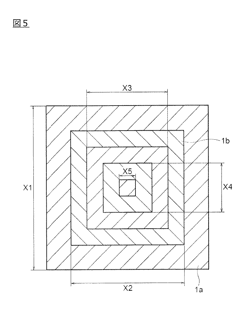
表1より、中心対称性を示す回折を生じる領域と、非中心対称性を示す回折を生じる領域とが存在し、所定の組成および平均イオン価数を満足している場合には、金属酸窒化物薄膜全体として残留分極を有する、すなわち、強誘電性を有していることが確認できた。 From Table 1, when a region showing diffraction showing central symmetry and a region causing diffraction showing non-central symmetry exist and satisfy a predetermined composition and average ionic valence, metal oxynitride. It was confirmed that the entire thin film had remanent polarization, that is, it had ferroelectricity.
1… 薄膜キャパシタ
51… 基板
52… 第1の電極
53… 金属酸窒化物薄膜
54… 第2の電極
15… 八面体
11… 酸素
12… 窒素
13… Bサイト原子
14… Aサイト原子
1 ...
Claims (6)
前記Aが、バリウム、ストロンチウムおよびランタンからなる群から選ばれる少なくとも1つであり、前記Bがタンタルおよびチタンからなる群から選ばれる少なくとも1つであり、
前記Aが前記ペロブスカイト構造におけるAサイトを占めた場合に示すイオン価数をa、前記Bが前記ペロブスカイト構造におけるBサイトを占めた場合に示すイオン価数をbとした場合、前記aおよびbが6.7≦a+b≦7.3である関係を満足し、
前記一般式中のxおよびyが、
2.000≦x≦3.275、
0.150≦y≦1.000である関係を満足し、
前記金属酸窒化物は、中心対称性を示す回折を生じる領域と、非中心対称性を示す回折を生じる領域と、を有する金属酸窒化物薄膜。 Is represented by the general formula ABO x N y, a metal oxynitride film containing metal oxynitride having the perovskite structure,
A is at least one selected from the group consisting of barium, strontium and lanthanum, and B is at least one selected from the group consisting of tantalum and titanium.
When the ionic valence indicated when A occupies the A site in the perovskite structure is a, and the ionic valence indicated when B occupies the B site in the perovskite structure is b, the a and b are Satisfying the relationship of 6.7 ≤ a + b ≤ 7.3,
X and y in the general formula are
2.000 ≤ x ≤ 3.275,
Satisfying the relationship of 0.150 ≤ y ≤ 1.000,
The metal oxynitride is a metal oxynitride thin film having a region that causes diffraction that exhibits central symmetry and a region that produces diffraction that exhibits non-central symmetry.
2.450≦x≦3.275、
0.150≦y≦0.700である関係を満足する請求項1から4のいずれかに記載の金属酸窒化物薄膜。 The x and the y are
2.450 ≤ x ≤ 3.275,
The metal oxynitride thin film according to any one of claims 1 to 4, which satisfies the relationship of 0.150 ≦ y ≦ 0.700.
Applications Claiming Priority (2)
| Application Number | Priority Date | Filing Date | Title |
|---|---|---|---|
| JP2020014760 | 2020-01-31 | ||
| JP2020014760 | 2020-01-31 |
Publications (2)
| Publication Number | Publication Date |
|---|---|
| JP2021123799A true JP2021123799A (en) | 2021-08-30 |
| JP7569698B2 JP7569698B2 (en) | 2024-10-18 |
Family
ID=77458401
Family Applications (1)
| Application Number | Title | Priority Date | Filing Date |
|---|---|---|---|
| JP2021010987A Active JP7569698B2 (en) | 2020-01-31 | 2021-01-27 | Metal oxynitride thin film and capacitor element |
Country Status (1)
| Country | Link |
|---|---|
| JP (1) | JP7569698B2 (en) |
Citations (5)
| Publication number | Priority date | Publication date | Assignee | Title |
|---|---|---|---|---|
| JP2010143788A (en) * | 2008-12-18 | 2010-07-01 | Canon Inc | Oxynitride piezoelectric material and method for producing the same |
| JP2013128073A (en) * | 2011-12-19 | 2013-06-27 | Canon Inc | Piezoelectric material, piezoelectric element, liquid discharging head, ultrasonic motor and dust removal device |
| WO2017135294A1 (en) * | 2016-02-01 | 2017-08-10 | Tdk株式会社 | Polycrystalline dielectric thin film and capacitor element |
| JP2018174305A (en) * | 2017-03-31 | 2018-11-08 | Tdk株式会社 | Polycrystal dielectric thin film and capacitive element |
| JP2019091888A (en) * | 2017-11-10 | 2019-06-13 | Tdk株式会社 | Metal oxynitride thin film, method for manufacturing the same, and capacitance element |
-
2021
- 2021-01-27 JP JP2021010987A patent/JP7569698B2/en active Active
Patent Citations (5)
| Publication number | Priority date | Publication date | Assignee | Title |
|---|---|---|---|---|
| JP2010143788A (en) * | 2008-12-18 | 2010-07-01 | Canon Inc | Oxynitride piezoelectric material and method for producing the same |
| JP2013128073A (en) * | 2011-12-19 | 2013-06-27 | Canon Inc | Piezoelectric material, piezoelectric element, liquid discharging head, ultrasonic motor and dust removal device |
| WO2017135294A1 (en) * | 2016-02-01 | 2017-08-10 | Tdk株式会社 | Polycrystalline dielectric thin film and capacitor element |
| JP2018174305A (en) * | 2017-03-31 | 2018-11-08 | Tdk株式会社 | Polycrystal dielectric thin film and capacitive element |
| JP2019091888A (en) * | 2017-11-10 | 2019-06-13 | Tdk株式会社 | Metal oxynitride thin film, method for manufacturing the same, and capacitance element |
Also Published As
| Publication number | Publication date |
|---|---|
| JP7569698B2 (en) | 2024-10-18 |
Similar Documents
| Publication | Publication Date | Title |
|---|---|---|
| EP2255397B1 (en) | Piezoelectric material | |
| US8518290B2 (en) | Piezoelectric material | |
| JP6296207B2 (en) | Dielectric thin film, capacitive element and electronic component | |
| TWI692439B (en) | Polycrystalline dielectric film and capacitor element | |
| JP2008537724A (en) | High power piezoelectric ceramic composition | |
| Kaur et al. | Optimization of sintering temperature for dielectric studies of La doped BZT ceramics | |
| KR102033058B1 (en) | Oxynitride thin film and capacitance element | |
| Li et al. | Relaxor behavior and Raman spectra of CuO-doped Pb (Mg1/3Nb2/3) O3-PbTiO3 ferroelectric ceramics | |
| JP6981280B2 (en) | Polycrystalline Dielectric Thin Films and Capacitive Devices | |
| CN114388693A (en) | Dielectric material, and device and memory device including the same | |
| JP7569698B2 (en) | Metal oxynitride thin film and capacitor element | |
| JP7000883B2 (en) | Oxynitride thin film and capacitive element | |
| TWI672283B (en) | NOx film and capacitor | |
| KR20180111687A (en) | Oxynitride thin film and capacitance element | |
| JPWO2019188435A1 (en) | Dielectric composition and electronic components | |
| JP7192383B2 (en) | Metal oxynitride thin film, method for producing metal oxynitride thin film, and capacitive element | |
| KR102103482B1 (en) | Polycrystalline dielectric thin film and capacitance element | |
| JP5605120B2 (en) | Dielectric ceramics for tunable devices | |
| JP7324458B2 (en) | Metal oxynitride powder and metal oxynitride sintered body | |
| Djoudi et al. | Influence of YTS addition on structural and electrical properties of PZT-based ceramics | |
| Ponomarev et al. | Ceramics with Ultrahigh Permittivity Values: Compositions, Synthesis Methods, and Properties at Low and Medium Frequencies | |
| CN109767915B (en) | Metal oxynitride thin film, method for producing metal oxynitride thin film, and capacitor element | |
| Rao et al. | New dielectric materials based on pyrochlore-type oxides-Ca3RE3Ti7Ta2O26. 5 (RE= Pr, Sm, Gd, Dy or Y): Structure, FT-IR spectra, microstructure and dielectric properties | |
| Dutta et al. | Synthesis and characterization of double-doped PZT piezoceramics | |
| Shah et al. | High permittivity and low dielectric loss analysis of lead free Sr1− x La x (Ti0. 5Fe0. 5) O3 |
Legal Events
| Date | Code | Title | Description |
|---|---|---|---|
| A621 | Written request for application examination |
Free format text: JAPANESE INTERMEDIATE CODE: A621 Effective date: 20230912 |
|
| A977 | Report on retrieval |
Free format text: JAPANESE INTERMEDIATE CODE: A971007 Effective date: 20240423 |
|
| A131 | Notification of reasons for refusal |
Free format text: JAPANESE INTERMEDIATE CODE: A131 Effective date: 20240528 |
|
| A521 | Request for written amendment filed |
Free format text: JAPANESE INTERMEDIATE CODE: A523 Effective date: 20240722 |
|
| TRDD | Decision of grant or rejection written | ||
| A01 | Written decision to grant a patent or to grant a registration (utility model) |
Free format text: JAPANESE INTERMEDIATE CODE: A01 Effective date: 20240925 |
|
| A61 | First payment of annual fees (during grant procedure) |
Free format text: JAPANESE INTERMEDIATE CODE: A61 Effective date: 20241007 |
|
| R150 | Certificate of patent or registration of utility model |
Ref document number: 7569698 Country of ref document: JP Free format text: JAPANESE INTERMEDIATE CODE: R150 |