JP2021534603A - Pixel sensor with adaptive exposure time - Google Patents
Pixel sensor with adaptive exposure time Download PDFInfo
- Publication number
- JP2021534603A JP2021534603A JP2020569765A JP2020569765A JP2021534603A JP 2021534603 A JP2021534603 A JP 2021534603A JP 2020569765 A JP2020569765 A JP 2020569765A JP 2020569765 A JP2020569765 A JP 2020569765A JP 2021534603 A JP2021534603 A JP 2021534603A
- Authority
- JP
- Japan
- Prior art keywords
- charge
- photodiode
- voltage
- adc
- capacitor
- Prior art date
- Legal status (The legal status is an assumption and is not a legal conclusion. Google has not performed a legal analysis and makes no representation as to the accuracy of the status listed.)
- Pending
Links
Images








Classifications
-
- G—PHYSICS
- G02—OPTICS
- G02B—OPTICAL ELEMENTS, SYSTEMS OR APPARATUS
- G02B27/00—Optical systems or apparatus not provided for by any of the groups G02B1/00 - G02B26/00, G02B30/00
- G02B27/01—Head-up displays
- G02B27/017—Head mounted
- G02B27/0172—Head mounted characterised by optical features
-
- G—PHYSICS
- G06—COMPUTING OR CALCULATING; COUNTING
- G06V—IMAGE OR VIDEO RECOGNITION OR UNDERSTANDING
- G06V10/00—Arrangements for image or video recognition or understanding
- G06V10/10—Image acquisition
- G06V10/12—Details of acquisition arrangements; Constructional details thereof
- G06V10/14—Optical characteristics of the device performing the acquisition or on the illumination arrangements
- G06V10/143—Sensing or illuminating at different wavelengths
-
- G—PHYSICS
- G06—COMPUTING OR CALCULATING; COUNTING
- G06V—IMAGE OR VIDEO RECOGNITION OR UNDERSTANDING
- G06V10/00—Arrangements for image or video recognition or understanding
- G06V10/10—Image acquisition
- G06V10/12—Details of acquisition arrangements; Constructional details thereof
- G06V10/14—Optical characteristics of the device performing the acquisition or on the illumination arrangements
- G06V10/147—Details of sensors, e.g. sensor lenses
-
- G—PHYSICS
- G06—COMPUTING OR CALCULATING; COUNTING
- G06V—IMAGE OR VIDEO RECOGNITION OR UNDERSTANDING
- G06V40/00—Recognition of biometric, human-related or animal-related patterns in image or video data
- G06V40/10—Human or animal bodies, e.g. vehicle occupants or pedestrians; Body parts, e.g. hands
- G06V40/18—Eye characteristics, e.g. of the iris
- G06V40/19—Sensors therefor
-
- H—ELECTRICITY
- H04—ELECTRIC COMMUNICATION TECHNIQUE
- H04N—PICTORIAL COMMUNICATION, e.g. TELEVISION
- H04N23/00—Cameras or camera modules comprising electronic image sensors; Control thereof
- H04N23/70—Circuitry for compensating brightness variation in the scene
- H04N23/73—Circuitry for compensating brightness variation in the scene by influencing the exposure time
-
- H—ELECTRICITY
- H04—ELECTRIC COMMUNICATION TECHNIQUE
- H04N—PICTORIAL COMMUNICATION, e.g. TELEVISION
- H04N25/00—Circuitry of solid-state image sensors [SSIS]; Control thereof
- H04N25/50—Control of the SSIS exposure
- H04N25/53—Control of the integration time
- H04N25/533—Control of the integration time by using differing integration times for different sensor regions
- H04N25/535—Control of the integration time by using differing integration times for different sensor regions by dynamic region selection
-
- H—ELECTRICITY
- H04—ELECTRIC COMMUNICATION TECHNIQUE
- H04N—PICTORIAL COMMUNICATION, e.g. TELEVISION
- H04N25/00—Circuitry of solid-state image sensors [SSIS]; Control thereof
- H04N25/50—Control of the SSIS exposure
- H04N25/57—Control of the dynamic range
- H04N25/58—Control of the dynamic range involving two or more exposures
- H04N25/581—Control of the dynamic range involving two or more exposures acquired simultaneously
- H04N25/583—Control of the dynamic range involving two or more exposures acquired simultaneously with different integration times
-
- H—ELECTRICITY
- H04—ELECTRIC COMMUNICATION TECHNIQUE
- H04N—PICTORIAL COMMUNICATION, e.g. TELEVISION
- H04N25/00—Circuitry of solid-state image sensors [SSIS]; Control thereof
- H04N25/50—Control of the SSIS exposure
- H04N25/57—Control of the dynamic range
- H04N25/59—Control of the dynamic range by controlling the amount of charge storable in the pixel, e.g. modification of the charge conversion ratio of the floating node capacitance
-
- H—ELECTRICITY
- H04—ELECTRIC COMMUNICATION TECHNIQUE
- H04N—PICTORIAL COMMUNICATION, e.g. TELEVISION
- H04N25/00—Circuitry of solid-state image sensors [SSIS]; Control thereof
- H04N25/70—SSIS architectures; Circuits associated therewith
- H04N25/76—Addressed sensors, e.g. MOS or CMOS sensors
- H04N25/77—Pixel circuitry, e.g. memories, A/D converters, pixel amplifiers, shared circuits or shared components
-
- H—ELECTRICITY
- H04—ELECTRIC COMMUNICATION TECHNIQUE
- H04N—PICTORIAL COMMUNICATION, e.g. TELEVISION
- H04N25/00—Circuitry of solid-state image sensors [SSIS]; Control thereof
- H04N25/70—SSIS architectures; Circuits associated therewith
- H04N25/76—Addressed sensors, e.g. MOS or CMOS sensors
- H04N25/77—Pixel circuitry, e.g. memories, A/D converters, pixel amplifiers, shared circuits or shared components
- H04N25/771—Pixel circuitry, e.g. memories, A/D converters, pixel amplifiers, shared circuits or shared components comprising storage means other than floating diffusion
-
- H—ELECTRICITY
- H04—ELECTRIC COMMUNICATION TECHNIQUE
- H04N—PICTORIAL COMMUNICATION, e.g. TELEVISION
- H04N25/00—Circuitry of solid-state image sensors [SSIS]; Control thereof
- H04N25/70—SSIS architectures; Circuits associated therewith
- H04N25/76—Addressed sensors, e.g. MOS or CMOS sensors
- H04N25/77—Pixel circuitry, e.g. memories, A/D converters, pixel amplifiers, shared circuits or shared components
- H04N25/772—Pixel circuitry, e.g. memories, A/D converters, pixel amplifiers, shared circuits or shared components comprising A/D, V/T, V/F, I/T or I/F converters
-
- H—ELECTRICITY
- H10—SEMICONDUCTOR DEVICES; ELECTRIC SOLID-STATE DEVICES NOT OTHERWISE PROVIDED FOR
- H10F—INORGANIC SEMICONDUCTOR DEVICES SENSITIVE TO INFRARED RADIATION, LIGHT, ELECTROMAGNETIC RADIATION OF SHORTER WAVELENGTH OR CORPUSCULAR RADIATION
- H10F39/00—Integrated devices, or assemblies of multiple devices, comprising at least one element covered by group H10F30/00, e.g. radiation detectors comprising photodiode arrays
- H10F39/80—Constructional details of image sensors
- H10F39/802—Geometry or disposition of elements in pixels, e.g. address-lines or gate electrodes
- H10F39/8023—Disposition of the elements in pixels, e.g. smaller elements in the centre of the imager compared to larger elements at the periphery
-
- H—ELECTRICITY
- H10—SEMICONDUCTOR DEVICES; ELECTRIC SOLID-STATE DEVICES NOT OTHERWISE PROVIDED FOR
- H10F—INORGANIC SEMICONDUCTOR DEVICES SENSITIVE TO INFRARED RADIATION, LIGHT, ELECTROMAGNETIC RADIATION OF SHORTER WAVELENGTH OR CORPUSCULAR RADIATION
- H10F39/00—Integrated devices, or assemblies of multiple devices, comprising at least one element covered by group H10F30/00, e.g. radiation detectors comprising photodiode arrays
- H10F39/80—Constructional details of image sensors
- H10F39/803—Pixels having integrated switching, control, storage or amplification elements
- H10F39/8037—Pixels having integrated switching, control, storage or amplification elements the integrated elements comprising a transistor
-
- G—PHYSICS
- G02—OPTICS
- G02B—OPTICAL ELEMENTS, SYSTEMS OR APPARATUS
- G02B27/00—Optical systems or apparatus not provided for by any of the groups G02B1/00 - G02B26/00, G02B30/00
- G02B27/01—Head-up displays
- G02B27/0101—Head-up displays characterised by optical features
- G02B2027/0112—Head-up displays characterised by optical features comprising device for genereting colour display
-
- G—PHYSICS
- G02—OPTICS
- G02B—OPTICAL ELEMENTS, SYSTEMS OR APPARATUS
- G02B27/00—Optical systems or apparatus not provided for by any of the groups G02B1/00 - G02B26/00, G02B30/00
- G02B27/01—Head-up displays
- G02B27/0101—Head-up displays characterised by optical features
- G02B2027/0118—Head-up displays characterised by optical features comprising devices for improving the contrast of the display / brillance control visibility
-
- G—PHYSICS
- G02—OPTICS
- G02B—OPTICAL ELEMENTS, SYSTEMS OR APPARATUS
- G02B27/00—Optical systems or apparatus not provided for by any of the groups G02B1/00 - G02B26/00, G02B30/00
- G02B27/01—Head-up displays
- G02B27/0101—Head-up displays characterised by optical features
- G02B2027/0138—Head-up displays characterised by optical features comprising image capture systems, e.g. camera
-
- G—PHYSICS
- G02—OPTICS
- G02B—OPTICAL ELEMENTS, SYSTEMS OR APPARATUS
- G02B27/00—Optical systems or apparatus not provided for by any of the groups G02B1/00 - G02B26/00, G02B30/00
- G02B27/01—Head-up displays
- G02B27/017—Head mounted
- G02B2027/0178—Eyeglass type
-
- G—PHYSICS
- G02—OPTICS
- G02B—OPTICAL ELEMENTS, SYSTEMS OR APPARATUS
- G02B27/00—Optical systems or apparatus not provided for by any of the groups G02B1/00 - G02B26/00, G02B30/00
- G02B27/01—Head-up displays
- G02B27/0179—Display position adjusting means not related to the information to be displayed
- G02B2027/0187—Display position adjusting means not related to the information to be displayed slaved to motion of at least a part of the body of the user, e.g. head, eye
-
- G—PHYSICS
- G02—OPTICS
- G02B—OPTICAL ELEMENTS, SYSTEMS OR APPARATUS
- G02B27/00—Optical systems or apparatus not provided for by any of the groups G02B1/00 - G02B26/00, G02B30/00
- G02B27/01—Head-up displays
- G02B27/0179—Display position adjusting means not related to the information to be displayed
-
- G—PHYSICS
- G02—OPTICS
- G02B—OPTICAL ELEMENTS, SYSTEMS OR APPARATUS
- G02B6/00—Light guides; Structural details of arrangements comprising light guides and other optical elements, e.g. couplings
- G02B6/0001—Light guides; Structural details of arrangements comprising light guides and other optical elements, e.g. couplings specially adapted for lighting devices or systems
- G02B6/0011—Light guides; Structural details of arrangements comprising light guides and other optical elements, e.g. couplings specially adapted for lighting devices or systems the light guides being planar or of plate-like form
- G02B6/0013—Means for improving the coupling-in of light from the light source into the light guide
- G02B6/0015—Means for improving the coupling-in of light from the light source into the light guide provided on the surface of the light guide or in the bulk of it
- G02B6/0016—Grooves, prisms, gratings, scattering particles or rough surfaces
-
- G—PHYSICS
- G02—OPTICS
- G02B—OPTICAL ELEMENTS, SYSTEMS OR APPARATUS
- G02B6/00—Light guides; Structural details of arrangements comprising light guides and other optical elements, e.g. couplings
- G02B6/0001—Light guides; Structural details of arrangements comprising light guides and other optical elements, e.g. couplings specially adapted for lighting devices or systems
- G02B6/0011—Light guides; Structural details of arrangements comprising light guides and other optical elements, e.g. couplings specially adapted for lighting devices or systems the light guides being planar or of plate-like form
- G02B6/0033—Means for improving the coupling-out of light from the light guide
- G02B6/0035—Means for improving the coupling-out of light from the light guide provided on the surface of the light guide or in the bulk of it
- G02B6/0036—2-D arrangement of prisms, protrusions, indentations or roughened surfaces
-
- G—PHYSICS
- G06—COMPUTING OR CALCULATING; COUNTING
- G06V—IMAGE OR VIDEO RECOGNITION OR UNDERSTANDING
- G06V20/00—Scenes; Scene-specific elements
- G06V20/20—Scenes; Scene-specific elements in augmented reality scenes
-
- H—ELECTRICITY
- H10—SEMICONDUCTOR DEVICES; ELECTRIC SOLID-STATE DEVICES NOT OTHERWISE PROVIDED FOR
- H10F—INORGANIC SEMICONDUCTOR DEVICES SENSITIVE TO INFRARED RADIATION, LIGHT, ELECTROMAGNETIC RADIATION OF SHORTER WAVELENGTH OR CORPUSCULAR RADIATION
- H10F39/00—Integrated devices, or assemblies of multiple devices, comprising at least one element covered by group H10F30/00, e.g. radiation detectors comprising photodiode arrays
- H10F39/10—Integrated devices
- H10F39/12—Image sensors
- H10F39/18—Complementary metal-oxide-semiconductor [CMOS] image sensors; Photodiode array image sensors
- H10F39/184—Infrared image sensors
- H10F39/1843—Infrared image sensors of the hybrid type
-
- H—ELECTRICITY
- H10—SEMICONDUCTOR DEVICES; ELECTRIC SOLID-STATE DEVICES NOT OTHERWISE PROVIDED FOR
- H10F—INORGANIC SEMICONDUCTOR DEVICES SENSITIVE TO INFRARED RADIATION, LIGHT, ELECTROMAGNETIC RADIATION OF SHORTER WAVELENGTH OR CORPUSCULAR RADIATION
- H10F39/00—Integrated devices, or assemblies of multiple devices, comprising at least one element covered by group H10F30/00, e.g. radiation detectors comprising photodiode arrays
- H10F39/10—Integrated devices
- H10F39/12—Image sensors
- H10F39/18—Complementary metal-oxide-semiconductor [CMOS] image sensors; Photodiode array image sensors
- H10F39/184—Infrared image sensors
- H10F39/1847—Multispectral infrared image sensors having a stacked structure, e.g. NPN, NPNPN or multiple quantum well [MQW] structures
-
- H—ELECTRICITY
- H10—SEMICONDUCTOR DEVICES; ELECTRIC SOLID-STATE DEVICES NOT OTHERWISE PROVIDED FOR
- H10F—INORGANIC SEMICONDUCTOR DEVICES SENSITIVE TO INFRARED RADIATION, LIGHT, ELECTROMAGNETIC RADIATION OF SHORTER WAVELENGTH OR CORPUSCULAR RADIATION
- H10F39/00—Integrated devices, or assemblies of multiple devices, comprising at least one element covered by group H10F30/00, e.g. radiation detectors comprising photodiode arrays
- H10F39/80—Constructional details of image sensors
- H10F39/805—Coatings
- H10F39/8053—Colour filters
-
- H—ELECTRICITY
- H10—SEMICONDUCTOR DEVICES; ELECTRIC SOLID-STATE DEVICES NOT OTHERWISE PROVIDED FOR
- H10F—INORGANIC SEMICONDUCTOR DEVICES SENSITIVE TO INFRARED RADIATION, LIGHT, ELECTROMAGNETIC RADIATION OF SHORTER WAVELENGTH OR CORPUSCULAR RADIATION
- H10F39/00—Integrated devices, or assemblies of multiple devices, comprising at least one element covered by group H10F30/00, e.g. radiation detectors comprising photodiode arrays
- H10F39/80—Constructional details of image sensors
- H10F39/806—Optical elements or arrangements associated with the image sensors
- H10F39/8063—Microlenses
-
- H—ELECTRICITY
- H10—SEMICONDUCTOR DEVICES; ELECTRIC SOLID-STATE DEVICES NOT OTHERWISE PROVIDED FOR
- H10F—INORGANIC SEMICONDUCTOR DEVICES SENSITIVE TO INFRARED RADIATION, LIGHT, ELECTROMAGNETIC RADIATION OF SHORTER WAVELENGTH OR CORPUSCULAR RADIATION
- H10F39/00—Integrated devices, or assemblies of multiple devices, comprising at least one element covered by group H10F30/00, e.g. radiation detectors comprising photodiode arrays
- H10F39/80—Constructional details of image sensors
- H10F39/811—Interconnections
Landscapes
- Engineering & Computer Science (AREA)
- Multimedia (AREA)
- Signal Processing (AREA)
- Physics & Mathematics (AREA)
- General Physics & Mathematics (AREA)
- Theoretical Computer Science (AREA)
- Health & Medical Sciences (AREA)
- General Health & Medical Sciences (AREA)
- Optics & Photonics (AREA)
- Vascular Medicine (AREA)
- Ophthalmology & Optometry (AREA)
- Human Computer Interaction (AREA)
- Transforming Light Signals Into Electric Signals (AREA)
- Solid State Image Pick-Up Elements (AREA)
- Photometry And Measurement Of Optical Pulse Characteristics (AREA)
Abstract
一例では、方法が、第1の電荷を生成するために、第1のフォトダイオードを入射光に露光することと、第2の電荷を生成するために、第2のフォトダイオードを入射光に露光することと、第1の電荷検知ユニットによって、第1の電荷を第1の電圧に変換することと、第2の電荷検知ユニットによって、第2の電荷を第2の電圧に変換することと、第1の電圧に基づいて、第1の電荷の量が飽和しきい値に達したことを検出し、第1の電荷の量が飽和しきい値に達したときの飽和時間を測定するように、ADCを制御することと、第1の電荷の量が飽和しきい値に達したことを検出したことに基づいて、入射光への第1のフォトダイオードおよび第2のフォトダイオードの露光を停止することと、第2の電圧に基づいて、露光が終了する前に第2のフォトダイオードによって生成された第2の電荷の量を測定するように、ADCを制御することとを含む。【選択図】図17In one example, the method exposes a first photodiode to incident light to generate a first charge and exposes a second photodiode to incident light to generate a second charge. The first charge detection unit converts the first charge to the first voltage, and the second charge detection unit converts the second charge to the second voltage. Detects that the amount of first charge has reached the saturation threshold based on the first voltage and measures the saturation time when the amount of first charge reaches the saturation threshold. , Stop exposure of the first and second photodiodes to incident light based on controlling the ADC and detecting that the amount of first charge has reached the saturation threshold. It involves controlling the ADC to measure the amount of second charge generated by the second photodiode before the end of exposure, based on the second voltage. [Selection diagram] FIG. 17
Description
関連出願
本特許出願は、2019年8月19日に出願された米国出願第16/544,136号および2018年8月20日に出願された米国仮出願第62/719,953号の優先権を主張する。米国出願第16/544,136号および米国出願第62/719,953号は、すべての目的のためにその全体が参照により本明細書に組み込まれる。
Related Applications This patent application is the priority of US Application Nos. 16 / 544,136 filed on August 19, 2019 and US Provisional Application Nos. 62 / 719,953 filed on August 20, 2018. Insist. US Application 16 / 544,136 and US Application 62 / 719,953 are incorporated herein by reference in their entirety for all purposes.
本開示は、一般に画像センサーに関し、より詳細には、画像生成のために光強度を決定するためのインターフェース回路要素を含むピクセルセル構造に関する。 The present disclosure relates generally to image sensors, and more particularly to pixel cell structures including interface circuit elements for determining light intensity for image generation.
画像センサー中の一般的なピクセルは、光子を電荷(たとえば、電子または正孔)に変換することによって入射光を検知するためのフォトダイオードを含む。入射光は、2D検知および3D検知など、異なる用途について異なる波長範囲の成分を含むことができる。その上、画像ひずみを低減するために、フォトダイオードのアレイの各フォトダイオードがグローバル露光期間において同時に入射光を検知して電荷を生成するグローバルシャッター動作が実施され得る。電荷は、電圧に変換するための電荷検知ユニット(たとえば、フローティングディフュージョン(floating diffusion))によって変換され得る。ピクセルセルのアレイは、電荷検知ユニットによって変換される電圧に基づいて入射光の異なる成分を測定し、シーンの2D画像および3D画像の生成のために測定結果を提供することができる。 Common pixels in image sensors include photodiodes for detecting incident light by converting photons into electric charges (eg, electrons or holes). The incident light can contain components in different wavelength ranges for different applications, such as 2D detection and 3D detection. Moreover, in order to reduce image distortion, a global shutter operation may be performed in which each photodiode in an array of photodiodes simultaneously detects incident light and generates charges during the global exposure period. Charges can be converted by a charge sensing unit (eg, floating diffusion) for conversion to voltage. An array of pixel cells can measure different components of incident light based on the voltage converted by the charge detection unit and provide measurement results for the generation of 2D and 3D images of the scene.
本開示は、画像センサーに関する。より詳細には、限定はしないが、本開示は、ピクセルセルに関する。本開示はまた、入射光の強度のデジタル表現を生成するためにピクセルセルの回路要素を動作させることに関する。 The present disclosure relates to an image sensor. In more detail, but not limited to, the present disclosure relates to pixel cells. The present disclosure also relates to operating the circuit elements of a pixel cell to generate a digital representation of the intensity of incident light.
一例では、装置が提供される。本装置は、第1の電荷を生成するための第1のフォトダイオードと、第2の電荷を生成するための第2のフォトダイオードと、第1の電荷を第1の電圧に変換するための第1の電荷検知ユニットと、第2の電荷を第2の電圧に変換するための第2の電荷検知ユニットと、飽和時間と電荷の量とを測定することが可能なADCと、コントローラとを備え、コントローラは、第1のフォトダイオードおよび第2のフォトダイオードを入射光に露光して、第1の電荷および第2の電荷をそれぞれ生成させることと、第1の電圧に基づいて、第1の電荷の量が飽和しきい値に達したことを検出し、第1の電荷の量が飽和しきい値に達したときの飽和時間を測定するために、ADCを第1の電荷検知ユニットに接続することと、第1の電荷の量が飽和しきい値に達したことを検出したことに基づいて、入射光への第1のフォトダイオードおよび第2のフォトダイオードの露光を停止することと、第2の電圧に基づいて、露光が終了する前に第2のフォトダイオードによって生成された第2の電荷の量を測定するために、ADCを第2の電荷検知ユニットに接続することとを行うように構成される。 In one example, a device is provided. The apparatus has a first photodiode for generating a first charge, a second photodiode for generating a second charge, and a first charge for converting the first charge into a first voltage. A first charge detection unit, a second charge detection unit for converting a second charge into a second voltage, an ADC capable of measuring the saturation time and the amount of charge, and a controller. The controller comprises exposing the first and second photodiodes to incident light to generate a first charge and a second charge, respectively, and a first, based on a first voltage. To detect that the amount of charge in the first charge has reached the saturation threshold and to measure the saturation time when the amount of first charge reaches the saturation threshold To connect and to stop the exposure of the first and second photodiodes to the incident light based on the detection that the amount of first charge has reached the saturation threshold. To measure the amount of second charge generated by the second photodiode before the end of exposure, based on the second voltage, connect the ADC to the second charge detection unit. Configured to do.
一態様では、本装置は、第1のフォトダイオードと第1の電荷シンクとの間に結合された第1のシャッタースイッチと、第2のフォトダイオードと第2の電荷シンクとの間に結合された第2のシャッタースイッチとをさらに備える。コントローラは、第1のシャッタースイッチおよび第2のシャッタースイッチを無効化することに基づいて、第1のフォトダイオードおよび第2のフォトダイオードを入射光に露光することと、第1のシャッタースイッチおよび第2のシャッタースイッチを有効化することに基づいて、入射光への第1のフォトダイオードおよび第2のフォトダイオードの露光を停止することとを行うように構成される。 In one aspect, the device is coupled between a first shutter switch coupled between a first photodiode and a first charge sink, and between a second photodiode and a second charge sink. It also has a second shutter switch. The controller exposes the first photodiode and the second photodiode to incident light based on disabling the first shutter switch and the second shutter switch, and the first shutter switch and the first shutter switch. Based on enabling the shutter switch of 2, it is configured to stop the exposure of the first photodiode and the second photodiode to the incident light.
一態様では、コントローラは、第1のフォトダイオードおよび第2のフォトダイオードのためのグローバルシャッタースイッチが第1の時間において開始し、第2の時間において終了するように、第1の時間において第1のシャッタースイッチおよび第2のシャッタースイッチを一緒に無効化し、第2の時間において第1のシャッタースイッチおよび第2のシャッタースイッチを一緒に有効化するように構成される。 In one aspect, the controller has a first time in the first time so that the global shutter switch for the first photodiode and the second photodiode starts in the first time and ends in the second time. The shutter switch and the second shutter switch are disabled together, and the first shutter switch and the second shutter switch are enabled together at the second time.
一態様では、第1の電荷検知ユニットおよび第2の電荷検知ユニットの各々は、それぞれ、第1のキャパシタおよび第2のキャパシタを含む。本装置は、第1のフォトダイオードと第1の電荷検知ユニットとの間に結合された第1の転送スイッチと、第2のフォトダイオードと第2の電荷検知ユニットとの間に結合された第2の転送スイッチとをさらに備える。コントローラは、第1の電荷を第1の電荷検知ユニットの第1のキャパシタに転送するように第1の転送スイッチを制御することと、第1の電荷を第1の電荷検知ユニットの第2のキャパシタに転送するように第2の転送スイッチを制御することと、第1の電荷および第2の電荷の転送が完了した後に、入射光への第1のフォトダイオードおよび第2のフォトダイオードの露光を停止することとを行うように構成される。 In one aspect, each of the first charge detection unit and the second charge detection unit includes a first capacitor and a second capacitor, respectively. In this device, the first transfer switch coupled between the first photodiode and the first charge detection unit, and the second coupled between the second photodiode and the second charge detection unit. It further includes 2 transfer switches. The controller controls the first transfer switch to transfer the first charge to the first capacitor of the first charge detection unit, and the first charge is transferred to the second charge detection unit of the first charge detection unit. Controlling the second transfer switch to transfer to a capacitor and exposing the first and second photodiodes to incident light after the transfer of the first and second charges is complete. Is configured to stop and do.
一態様では、コントローラは、第1の時間において、第1の電荷の第1のオーバーフロー電荷を貯蔵のために第1のフォトダイオードから第1の電荷検知ユニットに転送するために、第1のバイアス電圧において第1の転送スイッチをバイアスすることと、第1の時間において、第2の電荷の第2のオーバーフロー電荷を貯蔵のために第2のフォトダイオードから第2の電荷検知ユニットに転送するために、第1のバイアス電圧において第2の転送スイッチをバイアスすることと、第2の時間において、第1の電荷の第1の残留電荷を貯蔵のために第1のフォトダイオードから第1の電荷検知ユニットに転送するために、第2のバイアス電圧において第1の転送スイッチをバイアスすることと、第2の時間において、第2の電荷の第2の残留電荷を貯蔵のために第2のフォトダイオードから第2の電荷検知ユニットに転送するために、第2のバイアス電圧において第2の転送スイッチをバイアスすることとを行うように構成される。入射光への第1のフォトダイオードおよび第2のフォトダイオードの露光は、第1の残留電荷の転送と第2の残留電荷の転送とが完了した後に停止される。 In one aspect, the controller has a first bias to transfer the first overflow charge of the first charge from the first photodiode to the first charge sensing unit in the first time. To bias the first transfer switch in voltage and to transfer the second overflow charge of the second charge from the second photodiode to the second charge detection unit for storage in the first time. In addition, biasing the second transfer switch at the first bias voltage and, at the second time, the first charge from the first photodiode to store the first residual charge of the first charge. Biasing the first transfer switch at the second bias voltage to transfer to the detection unit and, at the second time, a second photodiode for storing the second residual charge of the second charge. It is configured to bias the second transfer switch at the second bias voltage in order to transfer from the diode to the second charge sensing unit. The exposure of the first photodiode and the second photodiode to the incident light is stopped after the transfer of the first residual charge and the transfer of the second residual charge are completed.
一態様では、第1の電荷検知ユニットは、第1のキャパシタとADCとの間に結合された第1の切替え可能バッファを含む。第2の電荷検知ユニットは、第1のキャパシタとADCとの間に結合された第2の切替え可能バッファを含む。コントローラは、第1の転送スイッチが第1のバイアス電圧においてバイアスされたとき、第1のオーバーフロー電荷の量が飽和しきい値を超えるかどうかを検出し、第1のオーバーフロー電荷の量が飽和しきい値に達したときの飽和時間を測定するように、ADCを制御するために、第1のスイッチバッファを有効化することと、入射光への第1のフォトダイオードおよび第2のフォトダイオードの露光が停止した後に、第2のキャパシタに貯蔵された第2の残留電荷の量を測定するようにADCを制御することとを行うように構成される。 In one aspect, the first charge sensing unit includes a first switchable buffer coupled between the first capacitor and the ADC. The second charge detection unit includes a second switchable buffer coupled between the first capacitor and the ADC. The controller detects whether the amount of the first overflow charge exceeds the saturation threshold when the first transfer switch is biased at the first bias voltage, and the amount of the first overflow charge saturates. To control the ADC to measure the saturation time when the threshold is reached, enable the first switch buffer and of the first and second photodiodes to the incident light. After the exposure is stopped, the ADC is configured to control the ADC to measure the amount of second residual charge stored in the second capacitor.
一態様では、第1のキャパシタは、第1のオーバーフロー電荷が第1のキャパシタに転送されたときに第1の電圧を生じさせる。ADCは、第1の電圧を、飽和しきい値を表す第1の静的しきい値電圧と比較することに基づいて、飽和時間を測定するように構成される。 In one aspect, the first capacitor produces a first voltage when the first overflow charge is transferred to the first capacitor. The ADC is configured to measure the saturation time based on comparing the first voltage with the first static threshold voltage representing the saturation threshold.
一態様では、第1のキャパシタは、第1の主キャパシタと第1の補助キャパシタとを含む。第1の残留電荷の転送より前に、コントローラは、第1の補助キャパシタを第1の主キャパシタから切断することと、第1の主キャパシタをリセットすることとを行うように構成される。第1の残留電荷は、第3の電圧を生成するために、第1の主キャパシタがリセットされた後に第1の主キャパシタに転送される。ADCは、第1の主キャパシタにおける第3の電圧を第1のランピングしきい値電圧と比較することに基づいて、第1の主キャパシタに貯蔵された第1の残留電荷の量を測定するように構成される。ADCは、第1の残留電荷の量を測定した後に、第4の電圧を生成するために、第1のオーバーフロー電荷の一部分を貯蔵する第1の補助キャパシタを第1の主キャパシタと接続することと、第4の電圧を第2のランピングしきい値電圧と比較することに基づいて第1のオーバーフロー電荷の量を測定することとを行うように構成される。コントローラは、第1の電圧、第3の電圧、または第4の電圧のうちの1つに基づいてADCによって生成された出力を選択するように構成される。選択は、第1の電圧が第1の静的しきい値電圧を越えるかどうかに基づき、第3の電圧が、第1のフォトダイオードの貯蔵容量を表す第2の静的しきい値電圧を越えるかどうかに基づく。コントローラは、第1のフォトダイオードによって受け取られた入射光の強度を表すために、選択された出力を提供するように構成される。 In one aspect, the first capacitor includes a first main capacitor and a first auxiliary capacitor. Prior to the transfer of the first residual charge, the controller is configured to disconnect the first auxiliary capacitor from the first main capacitor and reset the first main capacitor. The first residual charge is transferred to the first main capacitor after the first main capacitor is reset in order to generate a third voltage. The ADC will measure the amount of first residual charge stored in the first main capacitor based on comparing the third voltage in the first main capacitor with the first ramping threshold voltage. It is composed of. After measuring the amount of the first residual charge, the ADC connects the first auxiliary capacitor, which stores a portion of the first overflow charge, to the first main capacitor in order to generate a fourth voltage. And to measure the amount of the first overflow charge based on comparing the fourth voltage with the second ramping threshold voltage. The controller is configured to select the output produced by the ADC based on one of a first voltage, a third voltage, or a fourth voltage. The choice is based on whether the first voltage exceeds the first static threshold voltage, the third voltage is the second static threshold voltage representing the storage capacity of the first photodiode. Based on whether to exceed. The controller is configured to provide the output of choice to represent the intensity of the incident light received by the first photodiode.
一態様では、第2のキャパシタは、第2の主キャパシタと第2の補助キャパシタとを含む。第2の残留電荷の転送より前に、コントローラは、第2の補助キャパシタを第2の主キャパシタから切断することと、第2の主キャパシタをリセットすることとを行うように構成される。第2の残留電荷は、第2の電圧を生成するために、第2の主キャパシタがリセットされた後に第2の主キャパシタに転送される。ADCは、第2の主キャパシタにおける第2の電圧を第1のランピングしきい値電圧と比較することに基づいて、第2の主キャパシタに貯蔵された第2の残留電荷の量を測定するように構成される。ADCは、第2の残留電荷の量を測定した後に、第3の電圧を生成するために、第2のオーバーフロー電荷の一部分を貯蔵する第2の補助キャパシタを第2の主キャパシタと接続することと、第3の電圧を第2のランピングしきい値電圧と比較することに基づいて第2のオーバーフロー電荷の量を測定することとを行うように構成される。コントローラは、第2の電圧または第3の電圧のうちの1つに基づいてADCによって生成された出力を選択するように構成される。選択は、第2の電圧が、第2のフォトダイオードの貯蔵容量を表す静的しきい値電圧を越えるかどうかに基づく。コントローラは、第2のフォトダイオードによって受け取られた入射光の強度を表すために、選択された出力を提供するように構成される。 In one aspect, the second capacitor includes a second main capacitor and a second auxiliary capacitor. Prior to the transfer of the second residual charge, the controller is configured to disconnect the second auxiliary capacitor from the second main capacitor and reset the second main capacitor. The second residual charge is transferred to the second main capacitor after the second main capacitor has been reset in order to generate a second voltage. The ADC will measure the amount of second residual charge stored in the second main capacitor based on comparing the second voltage in the second main capacitor with the first ramping threshold voltage. It is composed of. After measuring the amount of second residual charge, the ADC connects a second auxiliary capacitor, which stores a portion of the second overflow charge, to the second main capacitor in order to generate a third voltage. And to measure the amount of the second overflow charge based on comparing the third voltage with the second ramping threshold voltage. The controller is configured to select the output produced by the ADC based on one of a second voltage or a third voltage. The choice is based on whether the second voltage exceeds the static threshold voltage, which represents the storage capacity of the second photodiode. The controller is configured to provide the output of choice to represent the intensity of the incident light received by the second photodiode.
一態様では、第1のフォトダイオードは、第1の波長範囲を有する入射光の第1の成分を検出するように構成される。第2のフォトダイオードは、第2の波長範囲を有する入射光の第2の成分を検出するように構成される。 In one aspect, the first photodiode is configured to detect a first component of incident light having a first wavelength range. The second photodiode is configured to detect a second component of incident light having a second wavelength range.
一態様では、第1の波長範囲と第2の波長範囲とは同等である。 In one aspect, the first wavelength range and the second wavelength range are equivalent.
一態様では、第1のフォトダイオードと第2のフォトダイオードとはピクセルセルの一部である。 In one aspect, the first photodiode and the second photodiode are part of a pixel cell.
一態様では、第1のフォトダイオードおよび第2のフォトダイオードは、それぞれ、第1のピクセルセルおよび第2のピクセルセルの一部である。 In one aspect, the first photodiode and the second photodiode are part of a first pixel cell and a second pixel cell, respectively.
一態様では、第1のピクセルセルと第2のピクセルセルとはピクセルセルアレイの一部である。第1のピクセルセルと第2のピクセルセルとは1つまたは複数のピクセルセルだけ離される。 In one aspect, the first pixel cell and the second pixel cell are part of a pixel cell array. The first pixel cell and the second pixel cell are separated by one or more pixel cells.
一例では、方法が提供される。本方法は、第1の電荷を生成するために、第1のフォトダイオードを入射光に露光することと、第2の電荷を生成するために、第2のフォトダイオードを入射光に露光することと、第1の電荷検知ユニットによって、第1の電荷を第1の電圧に変換することと、第2の電荷検知ユニットによって、第2の電荷を第2の電圧に変換することと、第1の電圧に基づいて、第1の電荷の量が飽和しきい値に達したことを検出し、第1の電荷の量が飽和しきい値に達したときの飽和時間を測定するように、ADCを制御することと、第1の電荷の量が飽和しきい値に達したことを検出したことに基づいて、入射光への第1のフォトダイオードおよび第2のフォトダイオードの露光を停止することと、第2の電圧に基づいて、露光が終了する前に第2のフォトダイオードによって生成された第2の電荷の量を測定するように、ADCを制御することとを含む。 In one example, a method is provided. In this method, a first photodiode is exposed to incident light to generate a first charge, and a second photodiode is exposed to incident light to generate a second charge. The first charge detection unit converts the first charge to the first voltage, and the second charge detection unit converts the second charge to the second voltage. To detect that the amount of first charge has reached the saturation threshold and measure the saturation time when the amount of first charge has reached the saturation threshold, based on the voltage of the ADC. And to stop the exposure of the first and second photodiodes to the incident light based on the detection that the amount of the first charge has reached the saturation threshold. And controlling the ADC to measure the amount of second charge generated by the second photodiode before the end of exposure, based on the second voltage.
一態様では、第1の電荷は、第1の波長範囲を有する入射光の第1の成分を検出することに基づいて第1のフォトダイオードによって生成される。第2の電荷は、第2の波長範囲を有する入射光の第2の成分を検出することに基づいて第2のフォトダイオードによって生成される。第1の波長範囲と第2の波長範囲とは異なる。 In one aspect, the first charge is generated by a first photodiode based on detecting a first component of incident light having a first wavelength range. The second charge is generated by the second photodiode based on detecting a second component of incident light having a second wavelength range. The first wavelength range and the second wavelength range are different.
以下の図を参照しながら、例示的な例が説明される。 An exemplary example will be illustrated with reference to the figures below.
図は、単に例証の目的で本開示の例を図示する。本開示の原理またはうたわれている利益から逸脱することなく、示される構造および方法の代替例が採用され得ることを、当業者は以下の説明から容易に認識されよう。 The figure illustrates an example of the present disclosure solely for purposes of illustration. Those skilled in the art will readily recognize from the following description that alternatives to the structures and methods shown may be adopted without departing from the principles or claims of the present disclosure.
添付の図において、同様の構成要素および/または特徴は、同じ参照ラベルを有し得る。さらに、同じタイプの様々な構成要素は、同様の構成要素間を区別するダッシュおよび第2のラベルを参照ラベルの後に続けることによって区別され得る。第1の参照ラベルのみが明細書において使用される場合、説明は、第2の参照ラベルには関係なく同じ第1の参照ラベルを有する同様の構成要素のいずれか1つに適用可能である。 In the attached figure, similar components and / or features may have the same reference label. In addition, various components of the same type can be distinguished by following a reference label with a dash and a second label that distinguish between similar components. If only the first reference label is used in the specification, the description is applicable to any one of the similar components having the same first reference label regardless of the second reference label.
以下の説明では、説明の目的で、いくつかの発明の例の完全な理解を提供するために、具体的な詳細が記載される。ただし、様々な例がこれらの具体的な詳細なしに実践され得ることは明らかであろう。図および説明は、限定するものではない。 In the following description, specific details are provided for purposes of illustration to provide a complete understanding of some examples of the invention. However, it will be clear that various examples can be practiced without these specific details. The figures and description are not limited.
一般的な画像センサーは、ピクセルセルのアレイを含む。各ピクセルセルは、光子を電荷(たとえば、電子または正孔)に変換することによって入射光の強度を測定するためのフォトダイオードを含む。フォトダイオードによって生成される電荷は、フローティングドレインノードを含むことができる電荷検知ユニットによって電圧に変換され得る。電圧は、アナログデジタル変換器(ADC)によってデジタル値に量子化され得る。デジタル値は、ピクセルセルによって受け取られた光の強度を表すことができ、シーンのスポットから受け取られた光に対応することができるピクセルを形成することができる。ピクセルのアレイを備える画像が、ピクセルセルのアレイのデジタル出力から導出され得る。 Typical image sensors include an array of pixel cells. Each pixel cell contains a photodiode for measuring the intensity of incident light by converting photons into electric charges (eg, electrons or holes). The charge generated by the photodiode can be converted to voltage by a charge sensing unit that can include a floating drain node. The voltage can be quantized into digital values by an analog-to-digital converter (ADC). The digital value can represent the intensity of the light received by the pixel cell and can form pixels that can correspond to the light received from the spots in the scene. An image with an array of pixels can be derived from the digital output of the array of pixel cells.
2D検知および3D検知など、撮像の異なるモードを実施するために、画像センサーが使用され得る。2D検知および3D検知は、異なる波長範囲の光に基づいて実施され得る。たとえば、2D検知のために可視光が使用され得、3D検知のために不可視光(たとえば、赤外光)が使用され得る。画像センサーは、異なる光波長範囲および色(たとえば、赤、緑、青、単色など)の可視光を、2D検知のために割り当てられたピクセルセルの第1のセットに与え、不可視光を、3D検知のために割り当てられたピクセルセルの第2のセットに与えるための光学フィルタアレイを含み得る。 Image sensors can be used to perform different modes of imaging, such as 2D detection and 3D detection. 2D and 3D detection can be performed based on light in different wavelength ranges. For example, visible light may be used for 2D detection and invisible light (eg, infrared light) may be used for 3D detection. The image sensor provides visible light in different light wavelength ranges and colors (eg, red, green, blue, monochromatic, etc.) to the first set of pixel cells assigned for 2D detection and invisible light in 3D. It may include an optical filter array to feed a second set of pixel cells assigned for detection.
2D検知を実施するために、ピクセルセルにおけるフォトダイオードは、ピクセルセルに入射する可視光成分(たとえば、赤、緑、青、単色など)の強度に比例するレートで電荷を生成することができ、露光期間において蓄積された電荷の量は、可視光(または、可視光のある色成分)の強度を表すために使用され得る。電荷は、フォトダイオードにおいて一時的に貯蔵され、次いで、電圧を生じさせるために、キャパシタ(たとえば、フローティングディフュージョン)に転送され得る。電圧は、可視光の強度に対応する出力を生成するために、アナログデジタル変換器(ADC)によってサンプリングおよび量子化され得る。可視光の異なる色成分(たとえば、赤色、緑色、および青色)を検知するように構成された複数のピクセルセルからの出力に基づいて、画像ピクセル値が生成され得る。 To perform 2D detection, photodiodes in a pixel cell can generate charges at a rate proportional to the intensity of visible light components (eg, red, green, blue, monochromatic, etc.) incident on the pixel cell. The amount of charge accumulated during the exposure period can be used to represent the intensity of visible light (or some color component of visible light). Charges can be temporarily stored in the photodiode and then transferred to a capacitor (eg, floating diffusion) to generate a voltage. The voltage can be sampled and quantized by an analog-to-digital converter (ADC) to produce an output corresponding to the intensity of visible light. Image pixel values can be generated based on the output from multiple pixel cells configured to detect different color components of visible light (eg, red, green, and blue).
その上、3D検知を実施するために、異なる波長範囲の光(たとえば、赤外光)が物体上に投影され得、反射された光が、ピクセルセルによって検出され得る。光は、構造化光、光パルスなどを含むことができる。ピクセルセル出力は、たとえば、反射された構造化光のパターンを検出すること、光パルスの飛行時間を測定することなどに基づいて、深度検知動作を実施するために使用され得る。反射された構造化光のパターンを検出するために、露光時間中にピクセルセルによって生成された電荷の量の分布が決定され得、電荷の量に対応する電圧に基づいてピクセル値が生成され得る。飛行時間測定のために、ピクセルセルのフォトダイオードにおける電荷の生成のタイミングが、反射された光パルスがピクセルセルにおいて受け取られた時間を表すように決定され得る。光パルスが物体に投影されたときと、反射された光パルスがピクセルセルにおいて受け取られたときとの間の時間差が、飛行時間測定を提供するために使用され得る。 Moreover, to perform 3D detection, light in different wavelength ranges (eg, infrared light) may be projected onto the object and the reflected light may be detected by the pixel cell. The light can include structured light, optical pulses, and the like. Pixel cell outputs can be used to perform depth sensing operations, for example, based on detecting the pattern of reflected structured light, measuring the flight time of an optical pulse, and so on. To detect the pattern of reflected structured light, the distribution of the amount of charge generated by the pixel cell during the exposure time can be determined and the pixel value can be generated based on the voltage corresponding to the amount of charge. .. For flight time measurements, the timing of charge generation in the photodiode of a pixel cell can be determined to represent the time the reflected light pulse is received in the pixel cell. The time difference between when the light pulse is projected onto the object and when the reflected light pulse is received in the pixel cell can be used to provide flight time measurements.
シーンの情報を生成するために、ピクセルセルアレイが使用され得る。いくつかの例では、アレイ内のピクセルセルのサブセット(たとえば、第1のセット)は、シーンの2D検知を実施するために光の可視成分を検出することができ、アレイ内のピクセルセルの別のサブセット(たとえば、第2のセット)は、シーンの3D検知を実施するために光の赤外線成分を検出することができる。2D撮像データと3D撮像データとの融合は、仮想現実(VR)体験、拡張現実(AR)体験および/または複合現実(MR)体験を提供する多くの用途に有用である。たとえば、ウェアラブルVR/AR/MRシステムは、システムのユーザが位置する環境のシーン再構築を実施し得る。再構築されたシーンに基づいて、VR/AR/MRは、インタラクティブ体験を提供するための表示効果を生成することができる。シーンを再構築するために、ピクセルセルアレイ内のピクセルセルのサブセットは、たとえば、環境中の物理的物体のセットを識別し、物理的物体とユーザとの間の距離を決定するために、3D検知を実施することができる。ピクセルセルアレイ内のピクセルセルの別のサブセットは、たとえば、これらの物理的物体のテクスチャ、色、および反射率を含む視覚属性をキャプチャするために、2D検知を実施することができる。シーンの2D画像データおよび3D画像データは、次いで、たとえば、物体の視覚属性を含むシーンの3Dモデルを作り出すためにマージされ得る。別の例として、ウェアラブルVR/AR/MRシステムは、2D画像データと3D画像データとの融合に基づいて、頭部追跡動作をも実施することができる。たとえば、2D画像データに基づいて、VR/AR/MRシステムは、物体を識別するために、いくつかの画像特徴を抽出することができる。3D画像データに基づいて、VR/AR/MRシステムは、ユーザによって着用されるウェアラブルデバイスに対する識別された物体のロケーションを追跡することができる。VR/AR/MRシステムは、たとえば、ユーザの頭部が移動するときの、ウェアラブルデバイスに対する識別された物体のロケーションの変化を追跡することに基づいて、頭部移動を追跡することができる。 Pixel cell array can be used to generate information about the scene. In some examples, a subset of pixel cells in the array (eg, the first set) can detect visible components of light to perform 2D detection of the scene, and another of the pixel cells in the array. A subset of (eg, a second set) can detect the infrared component of light to perform 3D detection of the scene. The fusion of 2D and 3D imaging data is useful in many applications that provide virtual reality (VR) experiences, augmented reality (AR) experiences and / or mixed reality (MR) experiences. For example, a wearable VR / AR / MR system may perform scene reconstruction of the environment in which the user of the system is located. Based on the reconstructed scene, VR / AR / MR can generate display effects to provide an interactive experience. To reconstruct the scene, a subset of pixel cells in a pixel cell array, for example, identify a set of physical objects in the environment and 3D detect to determine the distance between the physical object and the user. Can be carried out. Another subset of pixel cells within the pixel cell array can perform 2D detection, for example, to capture visual attributes including the texture, color, and reflectance of these physical objects. The 2D and 3D image data of the scene can then be merged, for example, to create a 3D model of the scene that includes the visual attributes of the object. As another example, the wearable VR / AR / MR system can also perform a head tracking motion based on the fusion of the 2D image data and the 3D image data. For example, based on 2D image data, a VR / AR / MR system can extract some image features to identify an object. Based on the 3D image data, the VR / AR / MR system can track the location of the identified object to the wearable device worn by the user. The VR / AR / MR system can track head movements, for example, based on tracking changes in the location of an identified object with respect to a wearable device as the user's head moves.
2D画像データと3D画像データとの相関を改善するために、ピクセルセルのアレイは、シーンのスポットからの入射光の異なる成分のコロケート(collocated)撮像を提供するように構成され得る。詳細には、各ピクセルセルは、複数のフォトダイオードと、複数の対応する電荷検知ユニットとを含むことができる。複数のフォトダイオードの各フォトダイオードは、入射光の異なる光成分を電荷に変換するように構成される。フォトダイオードが入射光の異なる光成分を受け取ることを可能にするために、フォトダイオードは、異なるフォトダイオードについて入射光のための異なる吸収距離を提供するスタックにおいて形成され得るか、または、光学フィルタのアレイの下の平面上に形成され得る。各電荷検知ユニットは、電荷を電圧に変換することによって対応するフォトダイオードの電荷を検知するための1つまたは複数のキャパシタを含み、電圧は、各フォトダイオードによって変換される入射光成分の強度のデジタル表現を生成するために、ADCによって量子化され得る。ADCは比較器を含む。量子化動作の一部として、比較器は、電圧を基準と比較して判定を出力することができる。比較器の出力は、メモリが自走カウンタからの値をいつ記憶するかを制御することができる。値は、電圧を量子化したことの結果を提供することができる。 To improve the correlation between the 2D image data and the 3D image data, the array of pixel cells may be configured to provide collated imaging of different components of incident light from a spot in the scene. In particular, each pixel cell can include a plurality of photodiodes and a plurality of corresponding charge sensing units. Each photodiode of a plurality of photodiodes is configured to convert different light components of incident light into electric charges. To allow a photodiode to receive different light components of incident light, the photodiode can be formed in a stack that provides different absorption distances for the incident light for different photodiodes, or of an optical filter. It can be formed on the plane below the array. Each charge detection unit contains one or more capacitors for detecting the charge of the corresponding photodiode by converting the charge to a voltage, where the voltage is the intensity of the incident light component converted by each photodiode. It can be quantized by the ADC to generate a digital representation. The ADC includes a comparator. As part of the quantization operation, the comparator can compare the voltage to the reference and output the determination. The output of the comparator can control when the memory stores the value from the self-propelled counter. The value can provide the result of quantizing the voltage.
ADCは、光強度測定動作のダイナミックレンジを増加させることができる、異なる強度範囲に関連付けられた異なる量子化動作に基づいて電圧を量子化することができる。詳細には、各フォトダイオードは、露光期間内にある量の電荷を生成することができ、電荷の量は入射光強度を表す。各フォトダイオードは、電荷の少なくとも一部を残留電荷として貯蔵するための量子ウェル(quantum well)をも有する。量子ウェル容量は、フォトダイオードと電荷検知ユニットとの間のスイッチ上のバイアス電圧に基づいて設定され得る。低光強度範囲では、フォトダイオードは、電荷の全体を残留電荷として量子ウェルに貯蔵することができる。PD ADC量子化動作では、ADCは、低光強度のデジタル表現を提供するために、残留電荷の量を検知することから電荷検知ユニットによって生成された第1の電圧を量子化することができる。残留電荷は、一般的に、フォトダイオードにおける暗電流をはるかに受けにくいので、低光強度測定の雑音フロアは低下され得、これは、ダイナミックレンジの下限をさらに拡張することができる。 The ADC can quantize the voltage based on different quantization operations associated with different intensity ranges that can increase the dynamic range of the light intensity measurement operation. In particular, each photodiode can generate a certain amount of charge within the exposure period, the amount of charge representing the incident light intensity. Each photodiode also has a quantum well for storing at least a portion of the charge as residual charge. The quantum well capacitance can be set based on the bias voltage on the switch between the photodiode and the charge sensing unit. In the low light intensity range, the photodiode can store the entire charge as residual charge in the quantum well. In the PD ADC quantization operation, the ADC can quantize the first voltage generated by the charge detection unit from detecting the amount of residual charge in order to provide a digital representation of low light intensity. Residual charges are generally much less susceptible to dark currents in photodiodes, so the noise floor of low light intensity measurements can be reduced, which can further extend the lower bound of the dynamic range.
その上、中光強度範囲では、量子ウェルは残留電荷によって飽和され得、フォトダイオードは、残りの電荷をオーバーフロー電荷として電荷検知ユニットに転送することができ、電荷検知ユニットは、オーバーフロー電荷の量を検知することから第2の電圧を生成することができる。FD ADC量子化動作では、ADCは、中光強度のデジタル表現を提供するために第2の電圧を量子化することができる。低光強度と中光強度の両方では、電荷検知ユニット中の1つまたは複数のキャパシタはまだ飽和されず、第1の電圧および第2の電圧の大きさは光強度と相関する。したがって、低光強度と中光強度の両方では、ADCの比較器は、第1の電圧または第2の電圧をランピング電圧と比較して判定を生成することができる。判定は、残留電荷またはオーバーフロー電荷の量を表すことができるカウンタ値を記憶するようにメモリを制御することができる。 Moreover, in the medium light intensity range, the quantum wells can be saturated with residual charge, the photodiode can transfer the remaining charge as overflow charge to the charge detection unit, and the charge detection unit will charge the amount of overflow charge. A second voltage can be generated from the detection. In the FD ADC quantization operation, the ADC can quantize a second voltage to provide a digital representation of medium light intensity. At both low and medium light intensities, one or more capacitors in the charge sensing unit are not yet saturated and the magnitude of the first and second voltages correlates with the light intensity. Thus, for both low and medium light intensities, the ADC comparator can compare the first or second voltage to the ramping voltage to generate a determination. The determination can control the memory to store a counter value that can represent the amount of residual or overflow charge.
高光強度範囲では、オーバーフロー電荷は、電荷検知ユニット中の1つまたは複数のキャパシタを飽和させることができる。その結果、第2の電圧の大きさはもはや光強度を追跡せず、光強度測定に非線形性が導入され得る。キャパシタの飽和によって引き起こされる非線形性を低減するために、ADCは、第2の電圧を静的しきい値と比較して判定を生成することによって、飽和までの時間(TTS:time−to−saturation)測定動作を実施することができ、判定は、カウンタ値を記憶するようにメモリを制御することができる。カウンタ値は、第2の電圧が飽和しきい値に達したときの時間を表すことができる。飽和までの時間は、電荷検知ユニットが飽和される範囲内の光の強度を表すことができ、第2の電圧の値は、もはや光の強度を反映しない。そのような仕組みにより、ダイナミックレンジの上限は拡張され得る。 In the high light intensity range, the overflow charge can saturate one or more capacitors in the charge detection unit. As a result, the magnitude of the second voltage no longer tracks the light intensity, and non-linearity can be introduced into the light intensity measurement. To reduce the non-linearity caused by capacitor saturation, the ADC compares the second voltage to a static threshold to generate a determination to generate a time to saturation (TTS: time-to-saturation). ) The measurement operation can be performed and the determination can control the memory to store the counter value. The counter value can represent the time when the second voltage reaches the saturation threshold. The time to saturation can represent the intensity of light within the range in which the charge sensing unit is saturated, and the value of the second voltage no longer reflects the intensity of light. By such a mechanism, the upper limit of the dynamic range can be extended.
ADCの比較器は、一般的に、特に上記で説明された複数の量子化動作を実施するとき、ピクセルセルのすべての他の構成要素の中で、最も大きい空間を占有し、最も多くの電力を消費する。したがって、電力とピクセルセルフットプリントとを低減するために、ピクセルセル内の複数の電荷検知ユニットの間で単一のADCが共有され得る。ピクセルセルのコントローラは、入射光の光成分の強度のデジタル表現を生成するために、TTS動作、FD ADC動作、およびPD ADC動作を実施するために単一のADCに接続することを交替で行うように、各電荷検知ユニットを制御することができる。しかしながら、そのような仕組みは、ピクセルセルの量子化動作の総時間ならびに画像フレームを生成するために必要とされるフレーム期間を実質的に増加させ得、これは、より低いフレームレートにつながり得る。これは、高速で変化する高速物体および/またはシーンの高解像度画像を提供する画像センサーの能力を劣化させ、画像センサーの用途を低減し得る。各フォトダイオードについての量子化動作の総時間を低減するために、コントローラは、TTS動作、FD ADC動作、およびPD ADC動作のサブセットのみを実施するように、フォトダイオードのうちのいくつかを構成することができる。たとえば、コントローラは、フォトダイオードのうちの1つの電荷検知ユニットをADCに接続し、TTS動作、FD ADC動作、およびPD ADC動作を実施するようにADCを制御することができる。コントローラは、次いで、他のフォトダイオードの他の電荷検知ユニットを連続的にADCに接続し、それらの電荷検知ユニットの出力についてPD ADC動作およびFD ADC動作を実施するにすぎないようにADCを制御することができる。フレーム期間を低減することに加えて、そのような仕組みはまた、ピクセルセル内のすべてのフォトダイオードが同じ露光期間を有することを保証することができ、これは、ローリングシャッター動作と同様に、明るい、高速に移動している物体を撮像するとき、シャッター効率を改善し、動きぼけおよびひずみを低減することができる。 ADC comparators generally occupy the largest space and have the most power of all other components of a pixel cell, especially when performing the multiple quantization operations described above. To consume. Therefore, a single ADC may be shared among multiple charge sensing units within a pixel cell to reduce power and pixel cell footprint. The controller of the pixel cell alternates connecting to a single ADC to perform TTS operation, FD ADC operation, and PD ADC operation to generate a digital representation of the intensity of the light component of the incident light. As such, each charge detection unit can be controlled. However, such a mechanism can substantially increase the total time of the quantization operation of the pixel cell as well as the frame period required to generate the image frame, which can lead to a lower frame rate. This can diminish the ability of image sensors to provide high resolution images of fast changing objects and / or scenes, reducing the use of image sensors. To reduce the total time of quantization operation for each photodiode, the controller configures some of the photodiodes to perform only a subset of TTS operation, FD ADC operation, and PD ADC operation. be able to. For example, the controller can connect the charge sensing unit of one of the photodiodes to the ADC and control the ADC to perform TTS operation, FD ADC operation, and PD ADC operation. The controller then continuously connects other charge sensing units of other photodiodes to the ADC and controls the ADC so that it only performs PD ADC and FD ADC operations on the outputs of those charge sensing units. can do. In addition to reducing the frame period, such a mechanism can also ensure that all photodiodes in a pixel cell have the same exposure period, which is as bright as rolling shutter operation. When imaging a fast-moving object, shutter efficiency can be improved and motion blur and distortion can be reduced.
ピクセルセルのフォトダイオードのサブセットの量子化動作を低減することは、ピクセルセルの量子化動作の総時間を低減し、フレームレートを増加させることができるが、そのような仕組みは、フォトダイオードのサブセットのダイナミックレンジの上限を低減し得る。詳細には、フォトダイオードのサブセットの電荷検知ユニットのキャパシタは、ピクセルセルが高強度光成分に露光されたとき、飽和し得る。しかし、それらのフォトダイオードについてTTS動作が実施されないので、ADCの量子化出力は、低光強度範囲および中光強度範囲についてのみ線形である。これは、それらのフォトダイオードについての光強度の測定可能な上限を低減し、それらのダイナミックレンジを低減する。その結果、ピクセルセルによる入射光の一部または全部の光成分の測定に非線形性が導入され得、これは、ピクセルセルアレイの、コレートされた2D/3D撮像動作だけでなく、グローバルシャッター動作をも劣化させる。 Reducing the quantization operation of a subset of photodiodes in a pixel cell can reduce the total time of quantization operation in a pixel cell and increase the frame rate, but such a mechanism is a subset of photodiodes. The upper limit of the dynamic range of can be reduced. Specifically, the capacitors in the charge sensing unit, which is a subset of photodiodes, can saturate when the pixel cells are exposed to high intensity light components. However, since no TTS operation is performed on those photodiodes, the ADC's quantization output is linear only for the low and medium light intensity ranges. This reduces the measurable upper limit of the light intensity for those photodiodes and reduces their dynamic range. As a result, non-linearity can be introduced in the measurement of some or all of the light components of the incident light by the pixel cell, which is not only the collated 2D / 3D imaging operation of the pixel cell array, but also the global shutter operation. Deteriorate.
本開示は、上記の問題点のうちの少なくともいくつかに対処することによって、改善されたコロケート2Dおよび3D撮像動作、ならびに改善されたグローバルシャッター動作を提供することができる画像センサーに関する。詳細には、画像センサーは、第1のフォトダイオードと、第2のフォトダイオードと、第1の電荷検知ユニットと、第2の電荷検知ユニットと、コントローラとを含み得る。第1のフォトダイオードは、入射光の第1の成分に応答して第1の電荷を生成することができる。第2のフォトダイオードは、入射光の第2の成分に応答して第2の電荷を生成することができる。第1の電荷検知ユニットおよび第2の電荷検知ユニットの各々は、フォトダイオードによって生成された電荷を貯蔵するために、フローティングドレインによって形成され得るキャパシタを含む。第1の電荷検知ユニットは、ADCを第2の電荷検知ユニットと共有することができる。共有方式の下で、ADCは、第1の電荷の量が飽和しきい値に達する飽和時間を測定するために第1の電荷検知ユニットの出力に対してTTS動作を実施し、その後に、第1の電荷の量を測定するためにPD ADC動作および/またはFD ADC動作を実施することになる。その上、ADCは、第2の電荷検知ユニットの出力に対してTTS動作を実施せず、第2の電荷の量を測定するために第2の電荷検知ユニットの出力に対してPD ADC動作および/またはFD ADC動作を実施するにすぎないことになる。 The present disclosure relates to an image sensor that can provide improved collage 2D and 3D imaging operations, as well as improved global shutter operation, by addressing at least some of the above problems. In particular, the image sensor may include a first photodiode, a second photodiode, a first charge detection unit, a second charge detection unit, and a controller. The first photodiode can generate a first charge in response to a first component of incident light. The second photodiode can generate a second charge in response to a second component of incident light. Each of the first charge detection unit and the second charge detection unit includes a capacitor that can be formed by a floating drain to store the charge generated by the photodiode. The first charge detection unit can share the ADC with the second charge detection unit. Under the shared method, the ADC performs a TTS operation on the output of the first charge sensing unit to measure the saturation time when the amount of first charge reaches the saturation threshold, and then the second. A PD ADC operation and / or an FD ADC operation will be performed to measure the amount of charge of 1. Moreover, the ADC does not perform a TTS operation on the output of the second charge detection unit, but a PD ADC operation on the output of the second charge detection unit to measure the amount of the second charge. / Or it will only perform the FD ADC operation.
コントローラは、それぞれ第1の電荷および第2の電荷を生成するために、第1のフォトダイオードおよび第2のフォトダイオードについての露光期間を開始することができる。画像センサーは、第1のフォトダイオードおよび第2のフォトダイオードの各々の間に結合されたシャッタースイッチと、第1の電荷および第2の電荷を排出することができる電荷シンクとを含み得る。露光期間は、シャッタースイッチを無効化することに基づいて開始され得る。コントローラは、飽和を検出し、飽和時間を測定するために、第1の電荷検知ユニットの出力に対してTTS動作を実施するように、ADCを制御することができる。飽和を検出すると、コントローラは、スイッチを有効化することに基づいて、第1のフォトダイオードおよび第2のフォトダイオードの露光期間を停止することができる。コントローラは、次いで、露光期間内に第2のフォトダイオードによって生成された第2の電荷の量を測定するために、第2の電荷検知ユニットの出力に対してPD ADC動作および/またはFD ADC動作を実施するように、ADCを制御することができる。コントローラはまた、TTS動作の後に、露光期間内に第1のフォトダイオードによって生成された第1の電荷の量を測定するために、第1の検知ユニットの出力に対してPD ADC動作および/またはFD ADC動作を実施するように、ADCを制御することができる。第1のフォトダイオードからの量子化出力と第2のフォトダイオードからの量子化出力とは、同じ画像フレーム、または同じフレーム期間のフレームの同じセット(たとえば、2Dおよび3Dフレーム)を形成することができる。 The controller can start the exposure period for the first photodiode and the second photodiode to generate a first charge and a second charge, respectively. The image sensor may include a shutter switch coupled between each of the first photodiode and the second photodiode, and a charge sink capable of discharging a first charge and a second charge. The exposure period can be started on the basis of disabling the shutter switch. The controller can control the ADC to perform a TTS operation on the output of the first charge sensing unit to detect saturation and measure saturation time. Upon detecting saturation, the controller can stop the exposure period of the first photodiode and the second photodiode based on enabling the switch. The controller then operates the PD ADC and / or FD ADC with respect to the output of the second charge sensing unit to measure the amount of second charge generated by the second photodiode during the exposure period. The ADC can be controlled to carry out. The controller also performs a PD ADC operation and / or with respect to the output of the first detection unit to measure the amount of first charge generated by the first photodiode during the exposure period after the TTS operation. The ADC can be controlled to perform the FD ADC operation. The quantized output from the first photodiode and the quantized output from the second photodiode may form the same image frame, or the same set of frames for the same frame period (eg, 2D and 3D frames). can.
いくつかの例では、第1のフォトダイオードと第2のフォトダイオードとはカーネルの一部であり得る。カーネルは、複数のピクセルセル、および/またはピクセルセルの複数のフォトダイオードを含むことができる。カーネルでは、フォトダイオードのグループがADCを共有することができる。マスタフォトダイオード(たとえば、第1のフォトダイオード)を除くグループ内のフォトダイオードのすべてが、PD ADC動作および/またはFD ADC動作のみを実施するためにADCへのアクセスを有するが、マスタフォトダイオードは、TTS動作、ならびにPD ADC動作および/またはFD ADC動作を実施するためにADCへのアクセスを有する。グループ内のすべてのフォトダイオードは、マスタフォトダイオードの電荷検知ユニットが飽和されたときに停止され得る同じ露光期間を有することができる。その結果、PD ADC動作および/またはFD ADC動作に基づく、それらのフォトダイオードの電荷検知ユニットの量子化結果は、依然として、妥当な忠実度で光成分の強度を表すことができる。一方、マスタフォトダイオードからの飽和の指示がない場合、フォトダイオードは、低光強度および中光強度の測定についての最小信号対雑音比を維持するために、事前構成された露光期間内に少なくともしきい値量の電荷を生成することができ、これは、ダイナミックレンジの下限を設定し得る。 In some examples, the first photodiode and the second photodiode may be part of the kernel. The kernel can include multiple pixel cells and / or multiple photodiodes in a pixel cell. In the kernel, a group of photodiodes can share the ADC. All photodiodes in the group except the master photodiode (eg, the first photodiode) have access to the ADC to perform only PD ADC and / or FD ADC operations, but the master photodiode does. , TTS operation, and PD ADC operation and / or has access to ADC to perform FD ADC operation. All photodiodes in the group can have the same exposure period which can be stopped when the charge sensing unit of the master photodiode is saturated. As a result, the quantization results of the charge sensing units of those photodiodes, based on PD ADC operation and / or FD ADC operation, can still represent the intensity of the optical component with reasonable fidelity. On the other hand, in the absence of saturation instructions from the master photodiode, the photodiode will at least within a preconfigured exposure period to maintain the minimum signal-to-noise ratio for low and medium light intensity measurements. A threshold amount of charge can be generated, which can set the lower bound of the dynamic range.
カーネルのフォトダイオードは、異なるピクセルセルからのものまたは同じピクセルセルからのものであり得、同じまたは異なる光成分を検出するように構成され得る。カーネル中のフォトダイオードのグループ化は、様々な方式に基づき得、用途固有であり得る。一例として、ピクセルのグループは、撮像されるべき所定の物体の輪郭/形状(たとえば、向きをもつ光源(pointed light source))に基づいて画定され得、ピクセルの各グループがカーネルを形成することができる。別の例として、同様の強度の光成分を受け取る可能性があるピクセルセルがカーネルを形成することができる。その上、ピクセルセルアレイ内のカーネルのフォトダイオードの空間分布は、画像センサーの用途に基づき得る。たとえば、受け取られたNIR光が少数のピクセルセルに集光されるように、画像センサーがシーンの小さい部分を撮像する場合、カーネルは、隣接するピクセルセルのフォトダイオードを含むことができる。一方、NIR光のパターンがピクセルセルにわたって疎に分布されるように、画像センサーがシーンの大きい部分を撮像する場合、カーネルは、離間されるピクセルセルのフォトダイオードを含むことができる。いくつかの例では、フォトダイオードのカーネルは、同じピクセルセルのフォトダイオードをも含むことができ、異なる波長範囲の光成分を検出するように構成され得る。そのような仕組みは、画像センサーが強い周辺光を伴う環境において動作するとき、およびピクセルセルの各フォトダイオードが高強度光成分を受け取ることができ、各フォトダイオードの電荷検知ユニットが飽和する可能性がある場合、有用であり得る。すべてのこれらのケースでは、カーネルのフォトダイオードは、同じ波長範囲または異なる波長範囲の光を検出するように構成され得る。 Kernel photodiodes can be from different pixel cells or from the same pixel cell and can be configured to detect the same or different light components. Grouping of photodiodes in the kernel can be based on various schemes and can be application specific. As an example, groups of pixels can be defined based on the contour / shape of a given object to be imaged (eg, a pointed light source), and each group of pixels can form a kernel. can. As another example, pixel cells that may receive light components of similar intensity can form the kernel. Moreover, the spatial distribution of kernel photodiodes within a pixel array can be based on the application of the image sensor. For example, if the image sensor captures a small portion of the scene such that the received NIR light is focused on a small number of pixel cells, the kernel can include photodiodes in adjacent pixel cells. On the other hand, if the image sensor captures a large portion of the scene so that the pattern of NIR light is sparsely distributed across the pixel cells, the kernel can include photodiodes in the pixel cells that are separated. In some examples, the photodiode kernel can also include photodiodes in the same pixel cell and may be configured to detect light components in different wavelength ranges. Such a mechanism is when the image sensor operates in an environment with strong ambient light, and each photodiode in the pixel cell can receive high intensity light components, which can saturate the charge sensing unit of each photodiode. If there is, it can be useful. In all these cases, kernel photodiodes may be configured to detect light in the same or different wavelength ranges.
各ピクセルセルが同じ露光期間を有する、本開示の実施形態では、グローバルシャッター動作が提供され得、各ピクセルセルは、コレートされた2Dおよび3D撮像動作をサポートするためにシーンの同じスポットから光の異なる成分を検出するために、複数のフォトダイオードを含む。その上、ピクセルセルのフォトダイオードは、カーネルであるかまたはカーネルに編成され、フォトダイオードの各カーネルは、ピクセルセルのサイズおよび電力消費を低減するために量子化動作を実施するためにADCを共有し、各カーネルのフォトダイオードの露光期間は、測定動作の線形性ならびに画像センサーのダイナミックレンジを改善するように動的に調整され得る。これらのすべては、画像センサーの性能を改善することができる。 In embodiments of the present disclosure, where each pixel cell has the same exposure period, a global shutter operation can be provided, where each pixel cell is of light from the same spot in the scene to support collated 2D and 3D imaging operations. Includes multiple photodiodes to detect different components. Moreover, the photodiodes of the pixel cell are either kernels or organized into kernels, and each photodiode kernel shares an ADC to perform quantization operations to reduce the size and power consumption of the pixel cells. However, the exposure period of the photodiode of each kernel can be dynamically adjusted to improve the linearity of the measurement operation as well as the dynamic range of the image sensor. All of these can improve the performance of the image sensor.
開示される技法は、人工現実システムを含むか、または人工現実システムに関連して実装され得る。人工現実は、ユーザへの提示の前に何らかの様式で調整された形式の現実であり、これは、たとえば、仮想現実(VR)、拡張現実(AR)、複合現実(MR)、ハイブリッド現実、あるいはそれらの何らかの組合せおよび/または派生物を含み得る。人工現実コンテンツは、完全に生成されたコンテンツ、またはキャプチャされた(たとえば、現実世界の)コンテンツと組み合わせられた生成されたコンテンツを含み得る。人工現実コンテンツは、ビデオ、オーディオ、触覚フィードバック、またはそれらの何らかの組合せを含み得、それらのいずれも、単一のチャネルまたは複数のチャネルにおいて提示され得る(観察者に3次元効果をもたらすステレオビデオなど)。加えて、いくつかの例では、人工現実は、たとえば、人工現実におけるコンテンツを作り出すために使用される、および/または人工現実において別様に使用される(たとえば、人工現実におけるアクティビティを実施する)アプリケーション、製品、アクセサリ、サービス、またはそれらの何らかの組合せにも関連付けられ得る。人工現実コンテンツを提供する人工現実システムは、ホストコンピュータシステムに接続されたヘッドマウントディスプレイ(HMD)、独立型HMD、モバイルデバイスまたはコンピューティングシステム、あるいは、1人または複数の観察者に人工現実コンテンツを提供することが可能な任意の他のハードウェアプラットフォームを含む、様々なプラットフォーム上に実装され得る。 The disclosed techniques may include or be implemented in connection with an artificial reality system. Artificial reality is a form of reality that has been adjusted in some way before being presented to the user, for example, virtual reality (VR), augmented reality (AR), mixed reality (MR), hybrid reality, or It may include any combination and / or derivative thereof. Artificial reality content can include fully generated content or generated content combined with captured (eg, real-world) content. Artificial reality content can include video, audio, haptic feedback, or any combination thereof, any of which can be presented in a single channel or multiple channels (such as stereo video that provides a three-dimensional effect to the observer). ). In addition, in some examples, artificial reality is used, for example, to create content in artificial reality, and / or otherwise used in artificial reality (eg, performing activities in artificial reality). It can also be associated with applications, products, accessories, services, or any combination thereof. An artificial reality system that provides artificial reality content is a head-mounted display (HMD) connected to a host computer system, a stand-alone HMD, a mobile device or computing system, or an artificial reality content for one or more observers. It can be implemented on a variety of platforms, including any other hardware platform that can be provided.
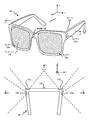
図1Aは、ニアアイディスプレイ100の一例の図である。ニアアイディスプレイ100は、ユーザにメディアを提示する。ニアアイディスプレイ100によって提示されるメディアの例は、1つまたは複数の画像、ビデオ、および/またはオーディオを含む。いくつかの例では、オーディオは、外部デバイス(たとえば、スピーカーおよび/またはヘッドフォン)を介して提示され、この外部デバイスは、ニアアイディスプレイ100、コンソール、またはその両方からオーディオ情報を受け取り、そのオーディオ情報に基づいてオーディオデータを提示する。ニアアイディスプレイ100は、概して、仮想現実(VR)ディスプレイとして動作するように構成される。いくつかの例では、ニアアイディスプレイ100は、拡張現実(AR)ディスプレイおよび/または複合現実(MR)ディスプレイとして動作するように変更される。
FIG. 1A is a diagram of an example of the
ニアアイディスプレイ100は、フレーム105とディスプレイ110とを含む。フレーム105は、1つまたは複数の光学要素に結合される。ディスプレイ110は、ユーザがニアアイディスプレイ100によって提示されたコンテンツを見るように構成される。いくつかの例では、ディスプレイ110は、1つまたは複数の画像からの光をユーザの眼に向けるための導波路ディスプレイアセンブリを備える。
The near-
ニアアイディスプレイ100は、画像センサー120a、120b、120c、および120dをさらに含む。画像センサー120a、120b、120c、および120dの各々は、異なる方向に沿った異なる視野を表す画像データを生成するように構成されたピクセルアレイを含み得る。たとえば、センサー120aおよび120bは、Z軸に沿った方向Aに向かう2つの視野を表す画像データを提供するように構成され得、センサー120cは、X軸に沿った方向Bに向かう視野を表す画像データを提供するように構成され得、センサー120dは、X軸に沿った方向Cに向かう視野を表す画像データを提供するように構成され得る。
The near-
いくつかの例では、センサー120a〜120dは、ニアアイディスプレイ100を装着したユーザにインタラクティブVR/AR/MR体験を提供するために、ニアアイディスプレイ100のディスプレイコンテンツを制御するかまたはニアアイディスプレイ100のディスプレイコンテンツに影響を与えるための入力デバイスとして構成され得る。たとえば、センサー120a〜120dは、ユーザが位置する物理的環境の物理的画像データを生成することができる。物理的画像データは、物理的環境におけるユーザのロケーションおよび/または移動の経路を追跡するためのロケーション追跡システムに提供され得る。システムは、次いで、インタラクティブ体験を提供するために、たとえば、ユーザのロケーションおよび向きに基づいて、ディスプレイ110に提供された画像データを更新することができる。いくつかの例では、ロケーション追跡システムは、ユーザが物理的環境内を移動するにつれて、物理的環境におけるおよびユーザの視野内の物体のセットを追跡するために、SLAMアルゴリズムを動作させ得る。ロケーション追跡システムは、物体のセットに基づいて物理的環境のマップを構築および更新し、マップ内のユーザのロケーションを追跡することができる。複数の視野に対応する画像データを提供することによって、センサー120a〜120dは、ロケーション追跡システムに物理的環境のより全体的なビューを提供することができ、これは、より多くの物体がマップの構築および更新に含まれることにつながり得る。そのような仕組みにより、物理的環境内のユーザのロケーションを追跡することの正確さおよびロバストネスが改善され得る。
In some examples, the
いくつかの例では、ニアアイディスプレイ100は、物理的環境に光を投影するための1つまたは複数のアクティブ照明器130をさらに含み得る。投影された光は、異なる周波数スペクトル(たとえば、可視光、赤外光、紫外光など)に関連付けられ得、様々な目的を果たすことができる。たとえば、照明器130は、たとえば、ユーザのロケーション追跡を可能にするために、センサー120a〜120dが暗い環境内の異なる物体の画像をキャプチャするのを支援するために、暗い環境において(または、低強度の赤外光、紫外光などを伴う環境において)光を投影し得る。照明器130は、ロケーション追跡システムがマップ構築/更新のために物体を識別するのを支援するために、環境内の物体上にいくつかのマーカーを投影し得る。
In some examples, the near-
いくつかの例では、照明器130は、立体撮像をも可能にし得る。たとえば、センサー120aまたは120bのうちの1つまたは複数は、可視光検知のための第1のピクセルアレイと赤外(IR)光検知のための第2のピクセルアレイの両方を含むことができる。第1のピクセルアレイは、色フィルタ(たとえば、バイエルフィルタ)でオーバーレイされ得、第1のピクセルアレイの各ピクセルが、特定の色(たとえば、赤色、緑色または青色のうちの1つ)に関連付けられた光の強度を測定するように構成される。また、(IR光検知のための)第2のピクセルアレイは、IR光の通過のみを可能にするフィルタでオーバーレイされ得、第2のピクセルアレイの各ピクセルが、IR光の強度を測定するように構成される。ピクセルアレイは、物体のRGB画像およびIR画像を生成することができ、IR画像の各ピクセルが、RGB画像の各ピクセルにマッピングされる。照明器130は、物体上にIRマーカーのセットを投影し得、その画像は、IRピクセルアレイによってキャプチャされ得る。画像に示されている物体のIRマーカーの分布に基づいて、システムは、IRピクセルアレイからの物体の異なる部分の距離を推定し、その距離に基づいて物体の立体画像を生成することができる。物体の立体画像に基づいて、システムは、たとえば、ユーザに対する物体の相対位置を決定することができ、インタラクティブ体験を提供するために、相対位置情報に基づいて、ディスプレイ100に提供された画像データを更新することができる。
In some examples, the
上記で説明されたように、ニアアイディスプレイ100は、極めて広範囲の光強度に関連する環境において動作され得る。たとえば、ニアアイディスプレイ100は、屋内環境または屋外環境において、および/あるいは1日の異なる時間において動作され得る。ニアアイディスプレイ100はまた、アクティブ照明器130がオンにされていてもいなくても動作し得る。その結果、画像センサー120a〜120dは、ニアアイディスプレイ100のための異なる動作環境に関連する極めて広範囲の光強度にわたって適切に動作すること(たとえば、入射光の強度と相関する出力を生成すること)が可能であるために、広いダイナミックレンジを有する必要があり得る。
As described above, the near-
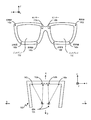
図1Bは、ニアアイディスプレイ100の別の例の図である。図1Bは、ニアアイディスプレイ100を装着したユーザの(1つまたは複数の)眼球135に面するニアアイディスプレイ100の側面を示す。図1Bに示されているように、ニアアイディスプレイ100は、複数の照明器140a、140b、140c、140d、140e、および140fをさらに含み得る。ニアアイディスプレイ100は、複数の画像センサー150aおよび150bをさらに含む。照明器140a、140b、および140cは、(図1Aの方向Aと反対である)方向Dに向かってある周波数範囲の光(たとえば、NIR)を放出し得る。放出された光は、あるパターンに関連付けられ得、ユーザの左眼球によって反射され得る。センサー150aは、反射された光を受け取り、反射パターンの画像を生成するためのピクセルアレイを含み得る。同様に、照明器140d、140e、および140fは、パターンを搬送するNIR光を放出し得る。NIR光は、ユーザの右眼球によって反射され得、センサー150bによって受け取られ得る。センサー150bも、反射パターンの画像を生成するためのピクセルアレイを含み得る。センサー150aおよび150bからの反射パターンの画像に基づいて、システムは、ユーザの注視点を決定し、ユーザにインタラクティブ体験を提供するために、決定された注視点に基づいて、ディスプレイ100に提供された画像データを更新することができる。
FIG. 1B is a diagram of another example of the near-
上記で説明されたように、ユーザの眼球に損傷を与えることを回避するために、照明器140a、140b、140c、140d、140e、および140fは、一般的に、極めて低強度の光を出力するように構成される。画像センサー150aおよび150bが図1Aの画像センサー120a〜120dと同じセンサーデバイスを備える場合、画像センサー120a〜120dは、入射光の強度が極めて低いときに入射光の強度と相関する出力を生成することが可能である必要があり得、これは、画像センサーのダイナミックレンジ要件をさらに増加させ得る。
As described above, in order to avoid damaging the user's eyeball, the
その上、画像センサー120a〜120dは、眼球の移動を追跡するために高速で出力を生成することが可能である必要があり得る。たとえば、ユーザの眼球は、ある眼球位置から別の眼球位置への素早いジャンプがあり得る極めて急速な移動(たとえば、サッカード運動(saccade movement))を実施することができる。ユーザの眼球の急速な移動を追跡するために、画像センサー120a〜120dは、高速で眼球の画像を生成する必要がある。たとえば、画像センサーが画像フレームを生成するレート(フレームレート)は、少なくとも、眼球の移動の速度に一致する必要がある。高いフレームレートは、画像フレームを生成することに関与するピクセルセルのすべてについての短い総露光時間、ならびに、画像生成のためにセンサー出力をデジタル値に変換するための高い速度を必要とする。その上、上記で説明されたように、画像センサーは、低光強度を伴う環境において動作することが可能である必要もある。
Moreover, the
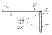
図2は、図1に示されているニアアイディスプレイ100の断面200の一例である。ディスプレイ110が、少なくとも1つの導波路ディスプレイアセンブリ210を含む。射出瞳230は、ユーザがニアアイディスプレイ100を装着したときにユーザの単一の眼球220がアイボックス(eyebox)領域中に配置されるロケーションである。例証の目的で、図2は、眼球220と単一の導波路ディスプレイアセンブリ210に関連する断面200を示すが、第2の導波路ディスプレイがユーザの第2の眼のために使用される。
FIG. 2 is an example of a
導波路ディスプレイアセンブリ210は、画像光を、射出瞳230に位置するアイボックスに、および眼球220に向けるように構成される。導波路ディスプレイアセンブリ210は、1つまたは複数の屈折率をもつ1つまたは複数の材料(たとえば、プラスチック、ガラスなど)から構成され得る。いくつかの例では、ニアアイディスプレイ100は、導波路ディスプレイアセンブリ210と眼球220との間に1つまたは複数の光学要素を含む。
The
いくつかの例では、導波路ディスプレイアセンブリ210は、制限はしないが、積層導波路ディスプレイ、可変焦点導波路ディスプレイなどを含む、1つまたは複数の導波路ディスプレイのスタックを含む。積層導波路ディスプレイは、それぞれの単色ソースが異なる色のものである導波路ディスプレイを積層することによって作り出された多色ディスプレイ(たとえば、赤緑青(RGB)ディスプレイ)である。積層導波路ディスプレイは、複数の平面上に投影され得る多色ディスプレイ(たとえば、多平面カラーディスプレイ)でもある。いくつかの構成では、積層導波路ディスプレイは、複数の平面上に投影され得る単色ディスプレイ(たとえば、多平面単色ディスプレイ)である。可変焦点導波路ディスプレイは、導波路ディスプレイから放出された画像光の焦点位置を調整することができるディスプレイである。代替例では、導波路ディスプレイアセンブリ210は、積層導波路ディスプレイと可変焦点導波路ディスプレイとを含み得る。
In some examples, the
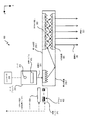
図3は、導波路ディスプレイ300の一例の等角図を示す。いくつかの例では、導波路ディスプレイ300は、ニアアイディスプレイ100の構成要素(たとえば、導波路ディスプレイアセンブリ210)である。いくつかの例では、導波路ディスプレイ300は、画像光を特定のロケーションに向ける何らかの他のニアアイディスプレイまたは他のシステムの一部である。
FIG. 3 shows an isometric view of an example of the
導波路ディスプレイ300は、ソースアセンブリ310と、出力導波路320と、コントローラ330とを含む。例証の目的で、図3は、単一の眼球220に関連付けられた導波路ディスプレイ300を示すが、いくつかの例では、導波路ディスプレイ300とは別個の、または部分的に別個の別の導波路ディスプレイが、ユーザの別の眼に画像光を提供する。
The
ソースアセンブリ310は、画像光355を生成する。ソースアセンブリ310は、画像光355を生成し、出力導波路320の第1の側面370−1上に位置する結合要素350に出力する。出力導波路320は、拡大された画像光340をユーザの眼球220に出力する光導波路である。出力導波路320は、第1の側面370−1上に位置する1つまたは複数の結合要素350において画像光355を受け取り、受け取られた入力画像光355を方向付け要素360に導く。いくつかの例では、結合要素350は、ソースアセンブリ310からの画像光355を出力導波路320に結合する。結合要素350は、たとえば、回折格子、ホログラフィック格子、1つまたは複数のカスケード型反射器、1つまたは複数のプリズム表面要素、および/またはホログラフィック反射器のアレイであり得る。
The
方向付け要素360は、受け取られた入力画像光355が分離要素365を介して出力導波路320から分離されるように、受け取られた入力画像光355を分離要素365に向け直す。方向付け要素360は、出力導波路320の第1の側面370−1の一部であるか、または出力導波路320の第1の側面370−1に取り付けられる。分離要素365は、方向付け要素360が分離要素365に対向するように、出力導波路320の第2の側面370−2の一部であるか、または出力導波路320の第2の側面370−2に取り付けられる。方向付け要素360および/または分離要素365は、たとえば、回折格子、ホログラフィック格子、1つまたは複数のカスケード型反射器、1つまたは複数のプリズム表面要素、および/またはホログラフィック反射器のアレイであり得る。
The
第2の側面370−2は、x次元およびy次元に沿った平面を表す。出力導波路320は、画像光355の内部全反射を促進する1つまたは複数の材料から構成され得る。出力導波路320は、たとえば、シリコン、プラスチック、ガラス、および/またはポリマーから構成され得る。出力導波路320は、比較的小さいフォームファクタを有する。たとえば、出力導波路320は、x次元に沿って幅約50mm、y次元に沿って長さ約30mm、およびz次元に沿って厚さ約0.5〜1mmであり得る。
The second side surface 370-2 represents a plane along the x and y dimensions. The
コントローラ330は、ソースアセンブリ310のスキャン動作を制御する。コントローラ330は、ソースアセンブリ310のためのスキャン命令を決定する。いくつかの例では、出力導波路320は、拡大された画像光340を大きい視野(FOV)でユーザの眼球220に出力する。たとえば、拡大された画像光340は、60度のおよび/またはそれよりも大きい、ならびに/あるいは150度のおよび/またはそれよりも小さい(xおよびyにおける)対角FOVでユーザの眼球220に提供される。出力導波路320は、20mm以上および/または50mm以下の長さ、ならびに/あるいは10mm以上および/または50mm以下の幅をもつアイボックスを提供するように構成される。
The
その上、コントローラ330は、画像センサー370によって提供される画像データに基づいて、ソースアセンブリ310によって生成される画像光355をも制御する。画像センサー370は、第1の側面370−1上に位置し得、たとえば、(たとえば、ロケーション決定のための)ユーザの前にある物理的環境の画像データを生成するために図1Aの画像センサー120a〜120dを含み得る。画像センサー370はまた、第2の側面370−2上に位置し得、ユーザの(たとえば、注視点決定のための)眼球220の画像データを生成するために図1Bの画像センサー150aおよび150bを含み得る。画像センサー370は、導波路ディスプレイ300内に位置しないリモートコンソールとインターフェースし得る。画像センサー370は、画像データをリモートコンソールに提供し得、リモートコンソールは、たとえば、ユーザのロケーション、ユーザの注視点などを決定し、ユーザに表示されるべき画像のコンテンツを決定し得る。リモートコンソールは、決定されたコンテンツに関係する命令をコントローラ330に伝送することができる。命令に基づいて、コントローラ330は、ソースアセンブリ310による画像光355の生成および出力を制御することができる。
Moreover, the
図4は、導波路ディスプレイ300の断面400の一例を示す。断面400は、ソースアセンブリ310と、出力導波路320と、画像センサー370とを含む。図4の例では、画像センサー370は、ユーザの前にある物理的環境の画像を生成するために、第1の側面370−1上に位置するピクセルセル402のセットを含み得る。いくつかの例では、ピクセルセル402のセットの露光を制御するために、ピクセルセル402のセットと物理的環境との間に挿入された機械的シャッター404があり得る。いくつかの例では、機械的シャッター404は、以下で説明されるように、電子シャッターゲートと置き換えられ得る。ピクセルセル402の各々は、画像の1つのピクセルに対応し得る。図4には示されていないが、ピクセルセル402の各々はまた、ピクセルセルによって検知されるべき光の周波数範囲を制御するために、フィルタでオーバーレイされ得ることを理解されたい。
FIG. 4 shows an example of a
リモートコンソールから命令を受け取った後に、機械的シャッター404は、露光期間において開き、ピクセルセル402のセットを露光することができる。露光期間中に、画像センサー370は、ピクセルセル402のセットに入射した光のサンプルを取得し、ピクセルセル402のセットによって検出された入射光サンプルの強度分布に基づいて画像データを生成することができる。画像センサー370は、次いで、画像データを、ディスプレイコンテンツを決定するリモートコンソールに提供し、ディスプレイコンテンツ情報をコントローラ330に提供することができる。コントローラ330は、次いで、ディスプレイコンテンツ情報に基づいて画像光355を決定することができる。
After receiving a command from the remote console, the mechanical shutter 404 can be opened during the exposure period to expose a set of
ソースアセンブリ310は、コントローラ330からの命令に従って画像光355を生成する。ソースアセンブリ310は、ソース410と光学システム415とを含む。ソース410は、コヒーレント光または部分的にコヒーレントな光を生成する光源である。ソース410は、たとえば、レーザーダイオード、垂直キャビティ面発光レーザー、および/または発光ダイオードであり得る。
The
光学システム415は、ソース410からの光を調節する1つまたは複数の光学的構成要素を含む。ソース410からの光を調節することは、たとえば、コントローラ330からの命令に従って拡大し、コリメートし、および/または向きを調整することを含み得る。1つまたは複数の光学的構成要素は、1つまたは複数のレンズ、液体レンズ、ミラー、開口、および/または格子を含み得る。いくつかの例では、光学システム415は、光ビームを液体レンズ外の領域にシフトするためにしきい値のスキャン角度を伴う光ビームのスキャンを可能にする複数の電極をもつ液体レンズを含む。光学システム415(同じくソースアセンブリ310)から放出される光は、画像光355と呼ばれる。
The
出力導波路320は、画像光355を受け取る。結合要素350は、ソースアセンブリ310からの画像光355を出力導波路320に結合する。結合要素350が回折格子である例では、内部全反射が出力導波路320中で発生し、画像光355が、分離要素365に向かって、(たとえば、内部全反射によって)出力導波路320中を内部的に伝搬するように、回折格子のピッチが選定される。
The
方向付け要素360は、出力導波路320から分離するために、画像光355を分離要素365のほうへ向け直す。方向付け要素360が回折格子である例では、回折格子のピッチは、入射画像光355が、分離要素365の表面に対して(1つまたは複数の)傾斜角において出力導波路320を出ることを引き起こすように選定される。
The
いくつかの例では、方向付け要素360および/または分離要素365は、構造的に同様である。出力導波路320を出た拡大された画像光340は、1つまたは複数の次元に沿って拡大される(たとえば、x次元に沿って延長され得る)。いくつかの例では、導波路ディスプレイ300は、複数のソースアセンブリ310と複数の出力導波路320とを含む。ソースアセンブリ310の各々は、原色(たとえば、赤、緑、または青)に対応する、波長の固有の帯域の単色画像光を放出する。出力導波路320の各々は、多色である拡大された画像光340を出力するために、離間距離を伴って一緒に積層され得る。
In some examples, the
図5は、ニアアイディスプレイ100を含むシステム500の一例のブロック図である。システム500は、各々制御回路要素510に結合された、ニアアイディスプレイ100と、撮像デバイス535と、入出力インターフェース540と、画像センサー120a〜120dおよび150a〜150bとを備える。システム500は、ヘッドマウントデバイス、ウェアラブルデバイスなどとして構成され得る。
FIG. 5 is a block diagram of an example of a
ニアアイディスプレイ100は、ユーザにメディアを提示するディスプレイである。ニアアイディスプレイ100によって提示されるメディアの例は、1つまたは複数の画像、ビデオ、および/またはオーディオを含む。いくつかの例では、オーディオは、外部デバイス(たとえば、スピーカーおよび/またはヘッドフォン)を介して提示され、この外部デバイスは、ニアアイディスプレイ100および/または制御回路要素510からオーディオ情報を受け取り、そのオーディオ情報に基づいてオーディオデータをユーザに提示する。いくつかの例では、ニアアイディスプレイ100はまた、ARアイウェアグラスとして働き得る。いくつかの例では、ニアアイディスプレイ100は、コンピュータ生成された要素(たとえば、画像、ビデオ、音など)を用いて、物理的現実世界の環境のビューを増強する。
The near-
ニアアイディスプレイ100は、導波路ディスプレイアセンブリ210、1つまたは複数の位置センサー525、および/または慣性測定ユニット(IMU)530を含む。導波路ディスプレイアセンブリ210は、ソースアセンブリ310と、出力導波路320と、コントローラ330とを含む。
The near-
IMU530は、位置センサー525のうちの1つまたは複数から受け取られた測定信号に基づいて、ニアアイディスプレイ100の初期位置に対するニアアイディスプレイ100の推定位置を指示する高速較正データを生成する電子デバイスである。
The
撮像デバイス535は、様々な用途のための画像データを生成し得る。たとえば、撮像デバイス535は、制御回路要素510から受け取られた較正パラメータに従って低速較正データを提供するために画像データを生成し得る。撮像デバイス535は、たとえば、ユーザのロケーション追跡を実施するために、ユーザが位置する物理的環境の画像データを生成するために図1Aの画像センサー120a〜120dを含み得る。撮像デバイス535は、たとえば、ユーザの関心物体を識別するために、ユーザの注視点を決定するための画像データを生成するために、図1Bの画像センサー150a〜150bをさらに含み得る。
The
入出力インターフェース540は、ユーザが制御回路要素510にアクション要求を送信することを可能にするデバイスである。アクション要求は、特定のアクションを実施するための要求である。たとえば、アクション要求は、アプリケーションを開始または終了するためのものであるか、あるいはアプリケーション内で特定のアクションを実施するためのものであり得る。
The input /
制御回路要素510は、撮像デバイス535、ニアアイディスプレイ100、および入出力インターフェース540のうちの1つまたは複数から受け取られた情報に従って、ユーザへの提示のためのメディアをニアアイディスプレイ100に提供する。いくつかの例では、制御回路要素510は、ヘッドマウントデバイスとして構成されたシステム500内に収容され得る。いくつかの例では、制御回路要素510は、システム500の他の構成要素と通信可能に結合された独立型コンソールデバイスであり得る。図5に示されている例では、制御回路要素510は、アプリケーションストア545と、追跡モジュール550と、エンジン555とを含む。
The
アプリケーションストア545は、制御回路要素510が実行するための1つまたは複数のアプリケーションを記憶する。アプリケーションは、プロセッサによって実行されたとき、ユーザへの提示のためのコンテンツを生成する命令のグループである。アプリケーションの例は、ゲームアプリケーション、会議アプリケーション、ビデオ再生アプリケーション、または他の好適なアプリケーションを含む。
The
追跡モジュール550は、1つまたは複数の較正パラメータを使用してシステム500を較正し、ニアアイディスプレイ100の位置の決定における誤差を低減するために、1つまたは複数の較正パラメータを調整し得る。
The
追跡モジュール550は、撮像デバイス535からの低速較正情報を使用して、ニアアイディスプレイ100の移動を追跡する。追跡モジュール550はまた、高速較正情報からの位置情報を使用して、ニアアイディスプレイ100の基準点の位置を決定する。
The
エンジン555は、システム500内でアプリケーションを実行し、追跡モジュール550から、ニアアイディスプレイ100の位置情報、加速度情報、速度情報、および/または予測された将来の位置を受け取る。いくつかの例では、エンジン555によって受け取られた情報は、ユーザに提示されるコンテンツのタイプを決定する導波路ディスプレイアセンブリ210への信号(たとえば、ディスプレイ命令)をもたらすために使用され得る。たとえば、インタラクティブ体験を提供するために、エンジン555は、(たとえば、追跡モジュール550によって提供される)ユーザのロケーション、または(たとえば、撮像デバイス535によって提供される画像データに基づく)ユーザの注視点、(たとえば、撮像デバイス535によって提供される画像データに基づく)物体とユーザとの間の距離に基づいて、ユーザに提示されるべきコンテンツを決定し得る。
The
図6は、画像センサー600の一例を示す。画像センサー600は、ニアアイディスプレイ100の一部であり得、ニアアイディスプレイ100のディスプレイコンテンツを制御するために、図5の制御回路要素510に2D画像データおよび3D画像データを提供することができる。図6に示されているように、画像センサー600は、ピクセルセル602aを含むピクセルセルのアレイ602を含み得る。ピクセルセル602aは、たとえば、フォトダイオード612a、612b、612c、および612dを含む複数のフォトダイオード612と、1つまたは複数の電荷検知ユニット614と、1つまたは複数のアナログデジタル変換器616とを含むことができる。複数のフォトダイオード612は、入射光の異なる成分を電荷に変換することができる。たとえば、フォトダイオード612a〜612cは、異なる可視光チャネルに対応することができ、ここで、フォトダイオード612aは、可視青色成分(たとえば、450〜490ナノメートル(nm)の波長範囲)を電荷に変換することができる。フォトダイオード612bは、可視緑色成分(たとえば、520〜560nmの波長範囲)を電荷に変換することができる。フォトダイオード612cは、可視赤色成分(たとえば、635〜700nmの波長範囲)を電荷に変換することができる。その上、フォトダイオード612dは、赤外線成分(たとえば、700〜1000nm)を電荷に変換することができる。1つまたは複数の電荷検知ユニット614の各々は、フォトダイオード612a〜612dによって生成された電荷を電圧に変換するために、電荷貯蔵デバイスとバッファとを含むことができ、その電圧は、1つまたは複数のADC616によってデジタル値に量子化され得る。フォトダイオード612a〜612cから生成されたデジタル値は、ピクセルの異なる可視光成分を表すことができ、各々は、特定の可視光チャネルにおける2D検知のために使用され得る。その上、フォトダイオード612dから生成されたデジタル値は、同じピクセルの赤外光成分を表すことができ、3D検知のために使用され得る。図6はピクセルセル602aが4つのフォトダイオードを含むことを示すが、ピクセルセルが異なる数のフォトダイオード(たとえば、2つ、3つなど)を含むことができることを理解されたい。
FIG. 6 shows an example of the image sensor 600. The image sensor 600 can be part of the near-
さらに、画像センサー600は、照明器622と、光学フィルタ624と、撮像モジュール628と、検知コントローラ630とをも含む。照明器622は、3D検知のために赤外光を投影することができる、レーザー、発光ダイオード(LED)など、赤外線照明器であり得る。投影された光は、たとえば、構造化光、光パルスなどを含み得る。光学フィルタ624は、ピクセルセル606aを含む各ピクセルセルの複数のフォトダイオード612a〜612d上にオーバーレイされるフィルタ要素のアレイを含み得る。各フィルタ要素は、ピクセルセル606aの各フォトダイオードによって受け取られた入射光の波長範囲を設定することができる。たとえば、フォトダイオード612a上のフィルタ要素は、可視青色光成分を伝送する一方、他の成分を遮断し得、フォトダイオード612b上のフィルタ要素は可視緑色光成分を伝送し得、フォトダイオード612c上のフィルタ要素は可視赤色光成分を伝送し得、フォトダイオード612d上のフィルタ要素は赤外光成分を伝送し得る。
Further, the image sensor 600 also includes an
画像センサー600は、撮像モジュール628をさらに含む。撮像モジュール628は、2D撮像動作を実施するための2D撮像モジュール632と、3D撮像動作を実施するための3D撮像モジュール634とをさらに含み得る。それらの動作は、ADC616によって提供されるデジタル値に基づき得る。たとえば、フォトダイオード612a〜612cの各々からのデジタル値に基づいて、2D撮像モジュール632は、各可視色チャネルについての入射光成分の強度を表すピクセル値のアレイを生成し、各可視色チャネルのための画像フレームを生成することができる。その上、3D撮像モジュール634は、フォトダイオード612dからのデジタル値に基づいて3D画像を生成することができる。いくつかの例では、デジタル値に基づいて、3D撮像モジュール634は、物体の表面によって反射された構造化光のパターンを検出し、検出されたパターンを、照明器622によって投影された構造化光のパターンと比較して、ピクセルセルアレイに対する表面の異なる点の深度を決定することができる。反射された光のパターンの検出のために、3D撮像モジュール634は、ピクセルセルにおいて受け取られた赤外光の強度に基づいてピクセル値を生成することができる。別の例として、3D撮像モジュール634は、照明器622によって伝送され、物体によって反射された赤外光の飛行時間に基づいて、ピクセル値を生成することができる。
The image sensor 600 further includes an image pickup module 628. The imaging module 628 may further include a 2D imaging module 632 for performing a 2D imaging operation and a 3D imaging module 634 for performing a 3D imaging operation. Their operation may be based on the digital values provided by
画像センサー600は、物体の2D撮像および3D撮像を実施するように画像センサー600の異なる構成要素を制御するための検知コントローラ640をさらに含む。次に図7A〜図7Cを参照すると、図7A〜図7Cは、2D撮像および3D撮像のための画像センサー600の動作の例を示す。図7Aは、2D撮像のための動作の一例を示す。2D撮像では、ピクセルセルアレイ602が、物体から反射された可視光を含む、環境における可視光を検出することができる。たとえば、図7Aを参照すると、可視光源700(たとえば、電球、太陽、または周囲可視光の他のソース)が、物体704上に可視光702を投影することができる。可視光706が、物体704のスポット708から反射され得る。可視光706は、周囲赤外光成分をも含むことができる。可視光706は、波長範囲w0、w1、w2、およびw3の可視光706の異なる成分を、それぞれ、ピクセルセル602aのフォトダイオード612a、612b、612c、および612dに通すように、光学フィルタアレイ624によってフィルタ処理され得る。波長範囲w0、w1、w2、およびw3は、それぞれ、青、緑、赤、および赤外線に対応することができる。図7Aに示されているように、赤外線照明器622がオンにされないとき、赤外線成分(w3)の強度は、周囲赤外光によって与えられ、極めて低くなり得る。その上、可視光706の異なる可視成分は、異なる強度をも有することができる。電荷検知ユニット614は、フォトダイオードによって生成された電荷を電圧に変換することができ、電圧は、ADC616によって、スポット708を表すピクセルの赤、青、および緑色成分を表すデジタル値に量子化され得る。図7Cを参照すると、デジタル値が生成された後に、検知コントローラ640は、デジタル値に基づいて、各々がフレーム期間714内のシーンの赤、青、または緑色画像のうちの1つを表す赤画像フレーム710a、青画像フレーム710b、および緑画像フレーム710cを含む、画像のセット710を含む画像のセットを生成するように、2D撮像モジュール632を制御することができる。各、赤画像からのピクセル(たとえば、ピクセル712a)、青画像からのピクセル(たとえば、ピクセル712b)、および緑画像からのピクセル(たとえば、ピクセル712c)は、シーンの同じスポット(たとえば、スポット708)からの光の可視成分を表すことができる。画像の異なるセット720が、後続のフレーム期間724において2D撮像モジュール632によって生成され得る。赤画像(たとえば、赤画像710a、720aなど)、青画像(たとえば、青画像710b、720bなど)、および緑画像(たとえば、緑画像710c、720cなど)の各々は、固有の色チャネルにおいて、および特定の時間においてキャプチャされたシーンの画像を表すことができ、たとえば、固有の色チャネルから画像特徴を抽出するためのアプリケーションに提供され得る。フレーム期間内にキャプチャされた各画像は同じシーンを表すことができ、画像の各対応するピクセルはシーンの同じスポットからの光を検出することに基づいて生成されるので、異なる色チャネル間の画像の対応が改善され得る。
The image sensor 600 further includes a detection controller 640 for controlling different components of the image sensor 600 to perform 2D and 3D imaging of the object. Next, referring to FIGS. 7A to 7C, FIGS. 7A to 7C show an example of the operation of the image sensor 600 for 2D imaging and 3D imaging. FIG. 7A shows an example of an operation for 2D imaging. In 2D imaging, the
さらに、画像センサー600は、物体704の3D撮像をも実施することができる。図7Bを参照すると、検知コントローラ610は、物体704上に、光パルス、構造化光などを含むことができる赤外光732を投影するように、照明器622を制御することができる。赤外光732は、700ナノメートル(nm)〜1ミリメートル(mm)の波長範囲を有することができる。赤外光734は、物体704のスポット708から反射することができ、ピクセルセルアレイ602のほうへ伝搬し、光学フィルタ624を通過することができ、光学フィルタ624は、電荷に変換するために(波長範囲w3の)赤外線成分をフォトダイオード612dに提供することができる。電荷検知ユニット614が電荷を電圧に変換することができ、電圧は、ADC616によってデジタル値に量子化され得る。図7Cを参照すると、デジタル値が生成された後に、検知コントローラ640は、デジタル値に基づいて、フレーム期間714内にキャプチャされた画像710の一部としてシーンの赤外線画像710dを生成するように、3D撮像モジュール634を制御することができる。その上、3D撮像モジュール634は、フレーム期間724内にキャプチャされた画像720の一部としてシーンの赤外線画像720dをも生成することができる。各赤外線画像は、異なるチャネル中であるが同じフレーム期間内にキャプチャされた他の画像と同じシーンを表すことができ(たとえば、赤外線画像710d対赤画像710a、青画像710b、および緑画像710c、赤外線画像720d対赤画像720a、青画像720b、および緑画像720cなど)、赤外線画像の各ピクセルは、同じフレーム期間内の他の画像中の他の対応するピクセルと同じ、シーンのスポットから赤外光を検出することに基づいて生成されるので、2D撮像と3D撮像との間の対応が同様に改善され得る。
Further, the image sensor 600 can also perform 3D imaging of the object 704. Referring to FIG. 7B, the detection controller 610 can control the
図8A〜図8Dは、ピクセルセル中のフォトダイオード612の配置の例を示す。図8Aに示されているように、ピクセルセル602a中のフォトダイオード612a〜612dは、ピクセルセル602aがスポット804aから入射光802を受け取る受光面800に直角である軸に沿ってスタックを形成することができる。たとえば、フォトダイオード612a〜612dは、受光面800がx軸およびy軸と平行であるとき、垂直軸(たとえば、z軸)に沿ってスタックを形成することができる。各フォトダイオードは、受光面800から異なる距離を有することができ、その距離は、入射光802の成分が各フォトダイオードによって吸収され、電荷に変換されるように設定することができる。たとえば、フォトダイオード612aは、受光面800に最も近く、青色成分を吸収し、電荷に変換することができ、青色成分は他の成分の中で最も短い波長範囲のものである。光812は、光802の残りの成分(たとえば、緑、赤、および赤外線)を含み、フォトダイオード612bに伝搬することができ、フォトダイオード612bは、緑色成分を吸収し、変換することができる。光822は、光812の残りの成分(たとえば、赤および赤外線)を含み、フォトダイオード612cに伝搬することができ、フォトダイオード612cは、赤色成分を吸収し、変換することができる。残りの赤外線成分832は、電荷に変換されるためにフォトダイオード612dに伝搬することができる。
8A-8D show an example of the arrangement of photodiodes 612 in a pixel cell. As shown in FIG. 8A, the
各フォトダイオード612a、612b、612c、および612dは、画像センサー600を形成するために積層され得る別個の半導体基板中にあり得る。たとえば、フォトダイオード612aは半導体基板840中にあり得、フォトダイオード612bは半導体基板842中にあり得、フォトダイオード612cは半導体基板844中にあり得、フォトダイオード612dは半導体基板846中にあり得る。各半導体基板は、スポット804bから光を受け取るためのピクセルセル602bなど、他のピクセルセルの他のフォトダイオードを含むことができる。画像センサー600は、ピクセルセル処理回路849を含むことができる別の半導体基板848を含むことができ、ピクセルセル処理回路849は、たとえば、電荷検知ユニット614、ADC616などを含むことができる。各半導体基板は、各フォトダイオードにおいて生成された電荷を処理回路849に転送するために、金属相互接続850、852、854、および856などの金属相互接続に接続され得る。
Each
図8B〜図8Dは、フォトダイオード612の他の例示的な配置を示す。図8B〜図8Dに示されているように、複数のフォトダイオード612は、受光面800と平行に横方向に配置され得る。図8Bの上の図表は、ピクセルセル602aの一例の側面図を示し、図8Bの下の図表は、ピクセルセル602aを含むピクセルアレイ602の上面図を示す。図8Bに示されているように、受光面800がx軸およびy軸と平行であることで、フォトダイオード612a、612b、612c、および612dは、半導体基板840中で同じくx軸およびy軸に沿って互いに隣接して配置され得る。ピクセルセル602aは、フォトダイオード上にオーバーレイされる光学フィルタアレイ860をさらに含む。光学フィルタアレイ860は光学フィルタ624の一部であり得る。光学フィルタアレイ860は、フォトダイオード612a、612b、612c、および612dの各々によって受け取られた入射光成分の波長範囲を設定するためにそれぞれのフォトダイオード上にオーバーレイされたフィルタ要素を含むことができる。たとえば、フィルタ要素860aは、フォトダイオード612a上にオーバーレイされ、可視青色光のみがフォトダイオード612aに入ることを可能にすることができる。その上、フィルタ要素860bは、フォトダイオード612b上にオーバーレイされ、可視緑色光のみがフォトダイオード612bに入ることを可能にすることができる。さらに、フィルタ要素860cは、フォトダイオード612c上にオーバーレイされ、可視赤色光のみがフォトダイオード612cに入ることを可能にすることができる。フィルタ要素860dは、フォトダイオード612d上にオーバーレイされ、赤外光のみがフォトダイオード612dに入ることを可能にすることができる。ピクセルセル602aは、光学フィルタアレイ860を介して受光面800の異なる横方向ロケーションにシーンのスポット(たとえば、スポット804a)からの光864を投影することができる1つまたは複数のマイクロレンズ862をさらに含み、これは、各フォトダイオードがピクセルセル602aのサブピクセルになり、ピクセルに対応する同じスポットからの光の成分を受け取ることを可能にする。ピクセルセル602aは、フォトダイオードによって生成された電荷からデジタル値を生成するための回路849(たとえば、電荷検知ユニット614、ADC616など)を含むことができる半導体基板848をも含むことができる。半導体基板840および848は、スタックを形成することができ、相互接続856と接続され得る。
8B-8D show other exemplary configurations of photodiode 612. As shown in FIGS. 8B-8D, the plurality of photodiodes 612 may be arranged laterally parallel to the
フォトダイオードが横方向に配置され、フォトダイオードによって受け取られた光成分を制御するために光学フィルタアレイが使用される、図8Bの配置は、多数の利点を与えることができる。たとえば、スタックの数および半導体基板の数が低減され得、これは、垂直高さだけでなく、半導体基板の間の相互接続をも低減する。その上、各フォトダイオードによって吸収される成分の波長範囲を設定するために光の伝搬距離ではなくフィルタ要素に依拠することは、波長範囲を選択する際のフレキシビリティを与えることができる。図8Cの上の図表に示されているように、ピクセルセルアレイ602は、異なるピクセルセルのための異なる光学フィルタアレイ860を含むことができる。たとえば、ピクセルセルアレイ602の各ピクセルセルは、フォトダイオード612aおよび612bのための(「M」でラベリングされた)380〜740nmの波長範囲の単色チャネルと、フォトダイオード612dのための(「NIR」でラベリングされた)700〜1000nmの波長範囲の赤外線チャネルとを提供する光学フィルタアレイを有することができる。しかし、光学フィルタアレイは、異なるピクセルセルについて異なる可視色チャネルをも提供し得る。たとえば、ピクセルセルアレイ602a、602b、602c、および602dのための光学フィルタアレイ860は、それぞれ、(「G」でラベリングされた)可視緑チャネルと、(「R」でラベリングされた)可視赤チャネルと、(「B」でラベリングされた)可視青チャネルと、ピクセルセルアレイのフォトダイオード612cのための可視緑チャネルとを提供し得る。別の例として、図8Cの下の図表に示されているように、各光学フィルタアレイ860は、各ピクセルセルアレイのフォトダイオード612bのための380〜1000nmの波長範囲に及ぶ(「M+NIR」とラベリングされた)単色および赤外線チャネルを提供することができる。
The arrangement of FIG. 8B, in which the photodiodes are arranged laterally and an optical filter array is used to control the optical components received by the photodiodes, can provide a number of advantages. For example, the number of stacks and the number of semiconductor substrates can be reduced, which reduces not only the vertical height but also the interconnection between the semiconductor substrates. Moreover, relying on the filter element rather than the propagation distance of light to set the wavelength range of the components absorbed by each photodiode can provide flexibility in selecting the wavelength range. As shown in the chart above FIG. 8C, the
図8Dは、図8Cに示されている例示的なチャネルを提供するための光学フィルタアレイ860の例を示す。図8Dに示されているように、光学フィルタアレイ860は、ピクセルセルアレイ内の各フォトダイオードによって受け取られた光の波長範囲を選択するために光学フィルタのスタックを含むことができる。たとえば、図8Dの上の図表を参照すると、光学フィルタ860aは、フォトダイオード612aのための単色チャネルを提供するためにスタックを形成する、全通過要素(all−pass element)870(たとえば、可視光と赤外光の両方を通す透明ガラス)と赤外線遮断要素872とを含むことができる。光学フィルタ860bも、同じくフォトダイオード612bのための単色チャネルを提供するために、全通過要素874と赤外線遮断要素876とを含むことができる。さらに、光学フィルタ860cは、フォトダイオード612cのための緑チャネルを提供するために、緑色可視光を通す(ただし、他の可視光成分を拒否する)緑通過要素(green−pass element)876と、赤外線遮断要素878とを含むことができる。最後に、光学フィルタ860dは、フォトダイオード612dのための赤外線チャネルを提供するために、全通過要素880と(可視光を遮断することができるが、赤外光が通り抜けることを可能にする)可視光遮断フィルタ882とを含むことができる。別の例では、図8Dの下の図表に示されているように、光学フィルタ860bは、フォトダイオード612bのための単色および赤外線チャネルを提供するために全通過要素872のみを含むことができる。
FIG. 8D shows an example of an
次に図9Aおよび図9Bを参照すると、図9Aおよび図9Bは、電荷検知ユニット614およびADC616の一例を含む、ピクセルセル602aの追加の構成要素を示す。図9Aに示されているように、ピクセルセル602aは、フォトダイオードPD(たとえば、フォトダイオード612a)と、シャッタースイッチM0と、転送スイッチM1と、電荷貯蔵デバイス902および切替え可能バッファ904を備える電荷検知ユニット614と、CCキャパシタ、比較器906、および出力論理回路908を備えるADC616とを含むことができる。比較器906の出力は、出力論理回路908を介して、ピクセルセル602aの内部または外部にあり得るメモリ912およびカウンタ914と結合される。ピクセルセル602は、スイッチ、電荷検知ユニット614、ならびにADC616を制御するためのコントローラ920をさらに含む。以下で説明されるように、コントローラ920は、フォトダイオードPDが、事前構成された露光期間内に入射光に基づいて電荷を蓄積することを可能にすることができる。コントローラ920はまた、露光停止信号922に基づいて、事前構成されたよりも早く、露光期間を停止することができる。その上、露光期間内に、コントローラ920は、入射光の強度のデジタル表現を生成するために異なる光強度範囲に関連付けられた複数の量子化動作を実施するように、電荷検知ユニット614およびADC616を制御することができる。コントローラ920は、複数の量子化動作のうちのどれが実施されるべきか(およびどれがスキップされるべきであるか)を選択するための選択信号924を受け取ることができる。選択は、入射光強度のデジタル表現を使用するアプリケーションをホストするホストデバイスからもたらされ得る。出力論理回路908は、どの量子化動作出力がメモリ912に記憶されるべきであり、および/またはピクセル値として出力されるべきであるかを決定することができる。コントローラ920は、ピクセルセル602aの内部にあるか、または検知コントローラ640の一部であり得る。各スイッチは、たとえば、金属酸化物半導体電界効果トランジスタ(MOSFET)、バイポーラ接合トランジスタ(BJT)など、トランジスタであり得る。
Next, with reference to FIGS. 9A and 9B, FIGS. 9A and 9B show additional components of
詳細には、シャッタースイッチM0は、露光期間を開始するためにコントローラ920によって提供されるAB信号によって無効化され得、露光期間において、フォトダイオードPDは、入射光に応答して電荷を生成および蓄積することができる。転送スイッチM1は、電荷の一部を電荷貯蔵デバイス902に転送するように、コントローラ920によって提供されるTG信号によって制御され得る。1つの量子化動作では、転送スイッチM1は、フォトダイオードPDの量子ウェル容量を設定するために、部分的にオンの状態においてバイアスされ得、これはまた、フォトダイオードPDにおいて貯蔵される残留電荷の量を設定する。フォトダイオードPDが残留電荷によって飽和された後に、オーバーフロー電荷は、転送スイッチM1を通って電荷貯蔵デバイス902に流れることができる。別の量子化動作では、転送スイッチM1は、測定のために残留電荷をフォトダイオードPDから電荷貯蔵デバイスに転送するために、完全にオンにされ得る。 Specifically, the shutter switch M0 can be disabled by the AB signal provided by the controller 920 to initiate the exposure period, during which the photodiode PD produces and stores charges in response to incident light. can do. The transfer switch M1 may be controlled by a TG signal provided by the controller 920 to transfer a portion of the charge to the charge storage device 902. In one quantization operation, the transfer switch M1 can be biased in the partially on state to set the quantum well capacitance of the photodiode PD, which is also the residual charge stored in the photodiode PD. Set the amount. After the photodiode PD is saturated with residual charge, the overflow charge can flow to the charge storage device 902 through the transfer switch M1. In another quantization operation, the transfer switch M1 may be turned on completely to transfer the residual charge from the photodiode PD to the charge storage device for measurement.
電荷貯蔵デバイス902は、構成可能な容量を有し、OFノードにおいて、スイッチM1から転送された電荷を電圧に変換することができる。電荷貯蔵デバイス902は、M6スイッチによって接続された、CFDキャパシタ(たとえば、フローティングドレイン)とCEXTキャパシタ(たとえば、MOSキャパシタ)とを含む。M6スイッチは、LG信号によって、CFDキャパシタとCEXTキャパシタとを並列に接続することによって電荷貯蔵デバイス902の容量を拡大すること、またはそれらのキャパシタを互いから切断することによって容量を低減することを可能にされ得る。電荷貯蔵デバイス902の容量は、電荷−電圧利得を増加させ、量子化誤差を低減するために、残留電荷の測定のために低減され得る。その上、電荷貯蔵デバイス902の容量はまた、飽和の可能性を低減し、非線形性を改善するために、オーバーフロー電荷の測定のために増加され得る。以下で説明されるように、電荷貯蔵デバイス902の容量は、異なる光強度範囲の測定のために調整され得る。電荷貯蔵デバイス902はまた、異なる量子化動作間でCFDキャパシタおよびCEXTキャパシタをリセットするための、コントローラ920によって提供されるリセット信号RSTによって制御され得るリセットスイッチM2と結合される。 The charge storage device 902 has a configurable capacity and can convert the charge transferred from the switch M1 into a voltage at the OF node. Charge storage device 902 includes connected by M6 switch, C FD capacitor (e.g., a floating drain) and C EXT capacitor (e.g., MOS capacitors) and. M6 switch, the LG signal, to expand the capacity of the charge storage device 902 by connecting the C FD capacitor and C EXT capacitor in parallel, or to reduce the capacitance by cutting them capacitor from one another Can be made possible. The capacity of the charge storage device 902 can be reduced for the measurement of residual charge in order to increase the charge-voltage gain and reduce the quantization error. Moreover, the capacity of the charge storage device 902 can also be increased for the measurement of overflow charge to reduce the possibility of saturation and improve the non-linearity. As described below, the capacitance of the charge storage device 902 can be adjusted for measurements in different light intensity ranges. Charge storage device 902 is also used to reset the C FD capacitor and C EXT capacitor between different quantization operation, is coupled to the reset switch M2 which may be controlled by a reset signal RST provided by the controller 920.
切替え可能バッファ904は、OFノードにおける電圧をバッファしてその駆動強度を改善するためのソースフォロワとして構成されたスイッチM3を含むことができる。バッファされた電圧は、ADC616の入力ノードPIXEL_OUTにおけるものであり得る。M4トランジスタは、切替え可能バッファ904のための電流源を提供し、VB信号によってバイアスされ得る。切替え可能バッファ904は、SEL信号によって有効化または無効化されるスイッチM5をも含む。スイッチM5が無効化されたとき、ソースフォロワM3は、PIXEL_OUTノードから切断され得る。以下で説明されるように、ピクセルセル602aは、切替え可能バッファ904を各々含む複数の電荷検知ユニット614を含み得、SEL信号に基づいて、一度に、電荷検知ユニットのうちの1つがPIXEL_OUT(およびADC616)と結合され得る。
The switchable buffer 904 can include a switch M3 configured as a source follower for buffering the voltage at the OF node and improving its drive strength. The buffered voltage can be at the input node PIXEL_OUT of the
上記で説明されたように、露光期間内にフォトダイオードPDによって生成された電荷は、電荷貯蔵デバイス902に一時的に貯蔵され、電圧に変換され得る。電圧は、電荷と入射光強度との間の所定の関係に基づいて入射光の強度を表すために量子化され得る。次に図10を参照すると、図10は、異なる光強度範囲についての時間に対する蓄積された電荷の量を示す。特定の時点において蓄積された電荷の総量は、露光期間内に図6のフォトダイオードPDに入射する光の強度を反映することができる。上記量は、露光期間が終了したときに測定され得る。入射光の強度についての低光強度範囲1006、中光強度範囲1008、および高光強度範囲1010を定義する電荷のしきい値の量について、しきい値1002およびしきい値1004が定義され得る。たとえば、総蓄積電荷(total accumulated charge)がしきい値1002未満である場合(たとえば、Q1)、入射光強度は低光強度範囲1006内にある。総蓄積電荷がしきい値1004としきい値1002との間にある場合(たとえば、Q2)、入射光強度は中光強度範囲1008内にある。総蓄積電荷がしきい値1004を超える場合、入射光強度は高光強度範囲1010内にある。低光強度範囲および中光強度範囲についての、蓄積された電荷の量は、フォトダイオードが低光強度範囲1006全体内で飽和せず、測定キャパシタが中光強度範囲1008全体内で飽和しない場合、入射光の強度と相関することができる。 As described above, the charge generated by the photodiode PD during the exposure period can be temporarily stored in the charge storage device 902 and converted into a voltage. The voltage can be quantized to represent the intensity of the incident light based on a given relationship between the charge and the intensity of the incident light. Next, with reference to FIG. 10, FIG. 10 shows the amount of charge accumulated over time for different light intensity ranges. The total amount of charge stored at a particular time point can reflect the intensity of the light incident on the photodiode PD of FIG. 6 during the exposure period. The amount may be measured at the end of the exposure period. Thresholds 1002 and 1004 may be defined for the amount of charge thresholds that define the low light intensity range 1006, medium light intensity range 1008, and high light intensity range 1010 for incident light intensity. For example, if the total accumulated charge is less than the threshold 1002 (eg, Q1), the incident light intensity is within the low light intensity range 1006. When the total stored charge is between the threshold 1004 and the threshold 1002 (eg Q2), the incident light intensity is within the medium light intensity range 1008. When the total stored charge exceeds the threshold 1004, the incident light intensity is within the high light intensity range 1010. The amount of accumulated charge for the low light intensity range and the medium light intensity range is when the photodiode does not saturate within the low light intensity range 1006 and the measurement capacitor does not saturate within the medium light intensity range 1008. It can correlate with the intensity of incident light.
低光強度範囲1006および中光強度範囲1008、ならびにしきい値1002および1004の定義は、フォトダイオードPDのフルウェル容量および電荷貯蔵デバイス902の容量に基づき得る。たとえば、低光強度範囲706は、露光期間の終了時の、フォトダイオードPDに貯蔵された残留電荷の総量が、フォトダイオードの貯蔵容量を下回るかまたはそれに等しくなるように定義され得、しきい値1002は、フォトダイオードPDのフルウェル容量に基づき得る。その上、中光強度範囲1008は、露光期間の終了時の、電荷貯蔵デバイス902に貯蔵された電荷の総量が、測定キャパシタの貯蔵容量を下回るかまたはそれに等しくなるように定義され得、しきい値1004は、電荷貯蔵デバイス902の貯蔵容量に基づき得る。一般的に、しきい値1004は、電荷貯蔵デバイス902に貯蔵された電荷の量が強度決定のために測定されたとき、測定キャパシタが飽和せず、測定された量が同じく入射光強度に関係することを保証するために、電荷貯蔵デバイス902のスケーリングされた貯蔵容量に基づき得る。以下で説明されるように、しきい値1002および1004は、フォトダイオードPDおよび電荷貯蔵デバイス902が飽和したかどうかを検出するために使用され得、これは、入射光の強度範囲を決定することができる。 The definitions of the low light intensity range 1006 and the medium light intensity range 1008, as well as the thresholds 1002 and 1004, can be based on the full well capacity of the photodiode PD and the capacity of the charge storage device 902. For example, the low light intensity range 706 can be defined so that at the end of the exposure period, the total amount of residual charge stored in the photodiode PD is less than or equal to the storage capacity of the photodiode, a threshold. 1002 may be based on the full well capacity of the photodiode PD. Moreover, the medium light intensity range 1008 can be defined such that the total amount of charge stored in the charge storage device 902 at the end of the exposure period is less than or equal to the storage capacity of the measurement capacitor. The value 1004 may be based on the storage capacity of the charge storage device 902. Generally, the threshold 1004 does not saturate the measurement capacitor when the amount of charge stored in the charge storage device 902 is measured for intensity determination, and the measured amount is also related to the incident light intensity. It may be based on the scaled storage capacity of the charge storage device 902 to ensure that it does. As described below, thresholds 1002 and 1004 can be used to detect whether the photodiode PD and charge storage device 902 are saturated, which determines the intensity range of incident light. Can be done.
さらに、入射光強度が高光強度範囲1010内にある場合、電荷貯蔵デバイス902において蓄積された総オーバーフロー電荷は、露光期間が終了する前にしきい値1004を超え得る。追加の電荷が蓄積されるにつれて、電荷貯蔵デバイス902は、露光期間の終了の前にフル容量に達し得、電荷漏洩が発生し得る。電荷貯蔵デバイス902がフル容量に達したことにより引き起こされる測定誤差を回避するために、電荷貯蔵デバイス902において蓄積された総オーバーフロー電荷がしきい値1004に達するのにかかる持続時間を測定するために、飽和までの時間測定が実施され得る。電荷貯蔵デバイス902における電荷蓄積のレートは、しきい値1004と飽和までの時間との間の比に基づいて決定され得、(キャパシタが無限の容量を有する場合に)露光期間の終了時に電荷貯蔵デバイス902において蓄積され得る電荷の仮定量(Q3)は、電荷蓄積のレートに従って外挿法によって決定され得る。電荷の仮定量(Q3)は、高光強度範囲1010内の入射光強度の合理的に正確な表現を提供することができる。 Further, if the incident light intensity is within the high light intensity range 1010, the total overflow charge accumulated in the charge storage device 902 may exceed the threshold 1004 before the end of the exposure period. As additional charge accumulates, the charge storage device 902 can reach full capacity before the end of the exposure period and charge leakage can occur. To measure the duration of the total overflow charge stored in the charge storage device 902 to reach the threshold 1004 to avoid measurement errors caused by the charge storage device 902 reaching full capacity. , Time to saturation can be measured. The rate of charge storage in the charge storage device 902 can be determined based on the ratio between the threshold 1004 and the time to saturation, and charge storage at the end of the exposure period (if the capacitor has an infinite capacity). The assumed amount of charge (Q3) that can be stored in the device 902 can be determined by the extrapolation method according to the rate of charge storage. The charge assumption (Q3) can provide a reasonably accurate representation of the incident light intensity within the high light intensity range 1010.
再び図9Aを参照すると、高光強度範囲1010と中光強度範囲1008とを測定するために、転送スイッチM1は、部分的にオンにされた状態においてTG信号によってバイアスされ得る。たとえば、転送スイッチM1のゲート電圧(TG)は、フォトダイオードPDのフルウェル容量に対応する、フォトダイオードにおいて生じたターゲット電圧に基づいて設定され得る。そのような仕組みにより、(高光強度範囲1010について)飽和までの時間、および/または(中光強度範囲1008について)電荷貯蔵デバイス902に貯蔵された電荷の量を測定するために、オーバーフロー電荷(たとえば、フォトダイオードが飽和した後にフォトダイオードによって生成された電荷)のみが、転送スイッチM1を通って移って電荷貯蔵デバイス902に達する。中光強度範囲および高光強度範囲の測定のために、(CEXTとCFDとを接続することによる)電荷貯蔵デバイス902のキャパシタンスはまた、しきい値1004を増加させるために最大化され得る。 Referring again to FIG. 9A, the transfer switch M1 may be biased by the TG signal in the partially turned on state to measure the high light intensity range 1010 and the medium light intensity range 1008. For example, the gate voltage (TG) of the transfer switch M1 may be set based on the target voltage generated in the photodiode, which corresponds to the full well capacitance of the photodiode PD. By such a mechanism, overflow charges (eg, for example) to measure the time to saturation (for the high light intensity range 1010) and / or the amount of charge stored in the charge storage device 902 (for the medium light intensity range 1008). Only the charge generated by the photodiode after the photodiode is saturated) is transferred through the transfer switch M1 to reach the charge storage device 902. For medium light intensity range and high light intensity range measurements, the capacitance of the charge storage device 902 (by connecting the C EXT and C FD ) can also be maximized to increase the threshold 1004.
その上、低光強度範囲1006を測定するために、転送スイッチM1は、フォトダイオードPDに貯蔵された残留電荷を電荷貯蔵デバイス902に転送するように、完全にオンにされた状態において制御され得る。転送は、電荷貯蔵デバイス902において貯蔵されたオーバーフロー電荷の量子化動作が完了した後に、および電荷貯蔵デバイス902がリセットされた後に、行われ得る。その上、電荷貯蔵デバイス902のキャパシタンスは低減され得る。上記で説明されたように、電荷貯蔵デバイス902のキャパシタンスの低減は、ある量の貯蔵された電荷についてより高い電圧を生じさせることができるように、電荷貯蔵デバイス902における電荷−電圧変換比を増加させることができる。より高い電荷−電圧変換比は、低光強度決定の正確さに対する後続の量子化動作によって導入される測定誤差(たとえば、量子化誤差、比較器オフセットなど)の効果を低減することができる。測定誤差は、量子化動作によって検出および/または弁別され得る最小電圧差に対する限界を設定することができる。電荷−電圧変換比を増加させることによって、最小電圧差に対応する電荷の量は低減され得、これは、ピクセルセル602aによる測定可能な光強度の下限を低減し、ダイナミックレンジを拡張する。
Moreover, in order to measure the low light intensity range 1006, the transfer switch M1 may be controlled in a fully turned-on state to transfer the residual charge stored in the photodiode PD to the charge storage device 902. .. The transfer may occur after the quantization operation of the overflow charge stored in the charge storage device 902 is completed and after the charge storage device 902 is reset. Moreover, the capacitance of the charge storage device 902 can be reduced. As described above, reducing the capacitance of the charge storage device 902 increases the charge-voltage conversion ratio in the charge storage device 902 so that a higher voltage can be generated for a certain amount of stored charge. Can be made to. Higher charge-voltage conversion ratios can reduce the effect of measurement errors introduced by subsequent quantization operations on the accuracy of low light intensity determination (eg, quantization error, comparator offset, etc.). The measurement error can set a limit to the minimum voltage difference that can be detected and / or discriminated by the quantization operation. By increasing the charge-voltage conversion ratio, the amount of charge corresponding to the minimum voltage difference can be reduced, which reduces the lower limit of measurable light intensity by the
電荷貯蔵デバイス902において蓄積された電荷(残留電荷および/またはオーバーフロー電荷)は、OFノードにおいてアナログ電圧を生じさせることができ、アナログ電圧は、PIXEL_OUTにおいて切替え可能バッファ904によってバッファされ、ADC616によって量子化され得る。図9Aに示されているように、ADC616は、スイッチM8によってリセットされ得る比較器906と、出力論理回路908とを含む。ADC616はまた、メモリ912およびカウンタ914と結合される。カウンタ914は、自走クロック信号に基づいてカウント値のセットを生成することができ、メモリ912は、カウンタ914によって生成されたカウント値(たとえば、最新のカウント値)を記憶するように、出力論理回路908を介して、比較器906によって制御され得る。メモリ912は、たとえば、以下で説明されるように、ローカルピクセル値に基づいてカウント値を記憶するためのラッチ回路であり得る。記憶されたカウント値は、入射光強度を表すために出力され得る。
The charge (residual charge and / or overflow charge) stored in the charge storage device 902 can generate an analog voltage at the OF node, which is buffered by the switchable buffer 904 at PIXEL_OUT and quantized by the
比較器906は、CCキャパシタによってPIXEL_OUTから導出されるアナログ電圧COMP_INをしきい値VREFと比較し、比較結果に基づいて判定VOUTを生成することができる。CCキャパシタは、PIXEL_OUT電圧におけるリセット雑音成分を相殺するために、COMP_IN電圧を生成するためにPIXEL_OUT電圧に追加され得る、VCC電圧におけるリセット雑音および比較器オフセット情報を記憶するために、雑音/オフセット補償方式で使用され得る。オフセット成分は、COMP_IN電圧中に残り、比較器906がCOMP_IN電圧をしきい値VREFと比較して判定VOUTを生成するとき、比較器906のオフセットによって相殺され得る。比較器906は、COMP_IN電圧がVREFに等しいかまたはVREFを超える場合、VOUTについて論理1を生成することができる。比較器906はまた、COMP_IN電圧がVREFを下回る場合、VOUTについて論理0を生成することができる。VOUTは、カウンタ914からのカウント値を記憶するようにメモリ912を制御するラッチ信号を制御することができる。
The comparator 906 can compare the analog voltage COMP_IN derived from PIXEL_OUT by the CC capacitor with the threshold value VREF, and generate a determination VOUT based on the comparison result. The CC capacitor is noise / offset compensated to store the reset noise and comparator offset information at the VCS voltage, which may be added to the PIXEL_OUT voltage to generate the COMP_IN voltage to offset the reset noise component at the PIXEL_OUT voltage. Can be used in a scheme. The offset component remains in the COMP_IN voltage and can be offset by the offset of the comparator 906 when the comparator 906 compares the COMP_IN voltage with the threshold VREF to generate a determination VOUT. The comparator 906 can generate
図11Aは、ADC616による飽和までの時間測定の一例を示す。飽和までの時間測定を実施するために、(ピクセルセル602aの外部にあり得る)しきい値生成器が、固定VREFを生成することができる。固定VREFは、電荷貯蔵デバイス902の飽和についての電荷量しきい値(たとえば、図10のしきい値1004)に対応する電圧に設定され得る。カウンタ914は、露光期間が開始した直後に(たとえば、シャッタースイッチM0が無効化された直後に)カウントすることを開始することができる。COMP_IN電圧が電荷貯蔵デバイス902におけるオーバーフロー電荷の蓄積によりランプダウンする(または実装形態に応じてランプアップする)とき、クロック信号は、カウンタ914におけるカウント値を更新するようにトグルし続ける。COMP_IN電圧は、ある時点において固定VREFしきい値に達し得、これは、VOUTが低から高に反転することを引き起こす。VOUTの変化はカウンタ914のカウンティングを停止し得、カウンタ914におけるカウント値は飽和までの時間を表し得る。
FIG. 11A shows an example of time measurement until saturation by
図11Bは、電荷貯蔵デバイス902において貯蔵された電荷の量の測定の一例を示す。測定が開始した後に、しきい値生成器は、(図11Bの例において)ランプアップするかまたは実装形態に応じてランプダウンすることができるランピングVREFを生成することができる。ランピングのレートは、カウンタ914に供給されるクロック信号の周波数に基づき得る。オーバーフロー電荷が測定される場合、ランピングVREFの電圧範囲は、しきい値1004(電荷貯蔵デバイス902の飽和についての電荷量しきい値)としきい値1002(フォトダイオードPDの飽和についての電荷量しきい値)との間にあり得、これは、中光強度範囲を定義することができる。残留電荷が測定される場合、ランピングVREFの電圧範囲は、しきい値1002に基づき、残留電荷測定のために電荷貯蔵デバイス902の低減された容量だけスケーリングされ得る。図11Bの例では、量子化プロセスは、VREFが各クロックサイクルについて同じ量だけ増加(または減少)する、一様量子化ステップで実施され得る。VREFの増加(または減少)の量は量子化ステップに対応する。VREFがCOMP_IN電圧の1つの量子化ステップ内に達したとき、比較器906のVOUTが反転し、これは、カウンタ914のカウンティングを停止することができ、カウント値は、1つの量子化ステップ内でCOMP_IN電圧に一致するように蓄積された量子化ステップの総数に対応することができる。カウント値は、電荷貯蔵デバイス902において貯蔵された電荷の量のデジタル表現、ならびに入射光強度のデジタル表現になり得る。 FIG. 11B shows an example of measuring the amount of charge stored in the charge storage device 902. After the measurement has started, the threshold generator can generate a ramping VREF that can be ramped up (in the example of FIG. 11B) or ramped down depending on the implementation. The ramping rate may be based on the frequency of the clock signal supplied to the counter 914. When the overflow charge is measured, the voltage range of the ramping VREF is the threshold 1004 (charge amount threshold for saturation of charge storage device 902) and threshold 1002 (charge amount threshold for photodiode PD saturation). Value), which can define a medium light intensity range. When the residual charge is measured, the voltage range of the ramping VREF can be scaled by the reduced capacitance of the charge storage device 902 for the residual charge measurement based on the threshold 1002. In the example of FIG. 11B, the quantization process can be performed in a uniform quantization step in which the VREF is increased (or decreased) by the same amount for each clock cycle. The amount of increase (or decrease) in VREF corresponds to the quantization step. When the VREF reaches within one quantization step of the COMP_IN voltage, the VOUT of the comparator 906 is inverted, which can stop the counting of the counter 914 and the count value is within one quantization step. It can correspond to the total number of quantization steps accumulated to match the COMP_IN voltage. The count value can be a digital representation of the amount of charge stored in the charge storage device 902, as well as a digital representation of the incident light intensity.
上記で説明されたように、ADC616は、(たとえば、量子化ステップの総数によって表される)ADC616によって出力された量レベルによって表される電荷の量と、ADC808による量レベルにマッピングされる電荷の実際の入力量との間に不一致があるとき、量子化誤差を導入することがある。量子化誤差は、より小さい量子化ステップサイズを使用することによって低減され得る。図11Bの例では、量子化誤差は、クロックサイクルごとにVREFの増加(または減少)の量だけ低減され得る。
As described above, the
量子化誤差は、より小さい量子化ステップサイズを使用することによって低減され得るが、エリアおよび実施速度は、量子化ステップがどの程度低減され得るかを限定し得る。より小さい量子化ステップサイズの場合、電荷量(および光強度)の特定の範囲を表すために必要とされる量子化ステップの総数は、増加し得る。増加された数の量子化ステップを表すためにより多数のデータビット(たとえば、255個のステップを表すために8ビット、127個のステップを表すために7ビットなど)が必要とされ得る。より多数のデータビットは、追加のバスがピクセル出力バス816に追加されることを必要とし得、これは、ピクセルセル601が、ヘッドマウントデバイスまたはごく限られたスペースをもつ他のウェアラブルデバイス上で使用される場合、実現可能でないことがある。その上、より多数の量子化ステップサイズの場合、ADC808は、(1つの量子化ステップと)一致する量レベルを見つける前により多数の量子化ステップを循環する必要があり得、これは、処理電力消費量および時間の増加、ならびに画像データを生成するレートの低減につながる。レートの低減は、高いフレームレートを必要とするいくつかのアプリケーション(たとえば、眼球の移動を追跡するアプリケーション)にとって許容できないことがある。 Quantization errors can be reduced by using smaller quantization step sizes, but areas and implementation rates can limit how much the quantization steps can be reduced. For smaller quantization step sizes, the total number of quantization steps required to represent a particular range of charge quantities (and light intensity) can be increased. More data bits (eg, 8 bits to represent 255 steps, 7 bits to represent 127 steps, etc.) may be required to represent the increased number of quantization steps. More data bits may require additional buses to be added to the pixel output bus 816, which means that pixel cell 601 is on a head-mounted device or other wearable device with very limited space. If used, it may not be feasible. Moreover, for a larger number of quantization step sizes, the ADC 808 may need to cycle through a larger number of quantization steps before finding a matching quantity level (with one quantization step), which is the processing power. This leads to increased consumption and time, as well as a reduction in the rate at which image data is generated. Rate reduction may be unacceptable for some applications that require high frame rates (eg, applications that track eye movements).
量子化誤差を低減するための1つのやり方は、量子化ステップが入力範囲にわたって一様でない非一様量子化方式を採用することによるものである。図11Cは、非一様量子化プロセスおよび一様量子化プロセスについてのADCコード(量子化プロセスの出力)と入力電荷量レベルとの間のマッピングの一例を示す。点線は、非一様量子化プロセスについてのマッピングを示し、実線は、一様量子化プロセスについてのマッピングを示す。一様量子化プロセスでは、(Δ1によって示される)量子化ステップサイズは、入力電荷量の範囲全体について同等である。対照的に、非一様量子化プロセスでは、量子化ステップサイズは、入力電荷量に応じて異なる。たとえば、(ΔSによって示される)低入力電荷量についての量子化ステップサイズは、(ΔLによって示される)大きい入力電荷量についての量子化ステップサイズよりも小さい。その上、同じ低入力電荷量について、非一様量子化プロセスについての量子化ステップサイズ(ΔS)は、一様量子化プロセスについての量子化ステップサイズ(Δ1)よりも小さくされ得る。 One way to reduce the quantization error is by adopting a non-uniform quantization method in which the quantization steps are not uniform over the input range. FIG. 11C shows an example of the mapping between the ADC code (output of the quantization process) and the input charge level for the non-uniform quantization process and the uniform quantization process. The dotted line shows the mapping for the non-uniform quantization process, and the solid line shows the mapping for the uniform quantization process. The uniform quantization process, the quantization step size (delta as indicated by the 1) is equivalent for the entire range of input charge amount. In contrast, in a non-uniform quantization process, the quantization step size depends on the amount of input charge. For example, (delta indicated by S) the quantization step size for low input charge amount is smaller than the quantization step size for large input charge quantity (indicated by delta L). Moreover, for the same low input charge amount, the quantization step size for the non-uniform quantization process (delta S) may be smaller than the quantization step size (delta 1) for uniform quantization process.
非一様量子化方式を採用することの1つの利点は、低入力電荷量を量子化するための量子化ステップが低減され得、これが、低入力電荷量を量子化する際の量子化誤差を低減し、ADC616によって弁別され得る最小入力電荷量が低減され得ることである。したがって、低減された量子化誤差は、画像センサーの測定可能な光強度の下限を押し下げることができ、ダイナミックレンジが増加され得る。その上、量子化誤差は高入力電荷量について増加されるが、量子化誤差は、高入力電荷量と比較して小さいままであり得る。したがって、電荷の測定に導入される全体的な量子化誤差は低減され得る。一方、入力電荷量の範囲全体をカバーする量子化ステップの総数は、同じ(さらには低減された)ままであり得、量子化ステップの数を増加させることに関連する上述の潜在的問題(たとえば、エリアの増加、処理速度の低減など)は、回避され得る。
One advantage of adopting the non-uniform quantization method can be to reduce the quantization step for quantizing the low input charge amount, which reduces the quantization error when quantizing the low input charge amount. It is possible to reduce and reduce the minimum amount of input charge that can be discriminated by the
図11Dは、非一様量子化プロセスを使用してピクセルADC808によってアナログ電圧を量子化することの一例を示す。(一様量子化プロセスを採用する)図11Bと比較して、VREFは、最初により緩やかな傾きで、および後でより急な傾きで、各クロックサイクルに関して非線形様式で増加する。傾きの差は、不均一な量子化ステップサイズに起因する。(より低い入力量範囲に対応する)より低いカウンタカウント値では、量子化ステップはより小さくされ、したがって、VREFは、より遅いレートで増加する。(より高い入力量範囲に対応する)より高いカウンタカウント値では、量子化ステップはより大きくされ、したがって、VREFは、より高いレートで増加する。非一様なVREFの傾きは、たとえば、カウンタ814のカウンティングの頻度を変更すること、VREF電圧とカウンタ914のカウント値との間の関係を変更することなどに基づいて生成され得る。いくつかの例では、図11Dの非一様量子化プロセスは、低光強度範囲1006および中光強度範囲1008についての光強度決定のために採用され得る。 FIG. 11D shows an example of quantizing an analog voltage with a pixel ADC808 using a non-uniform quantization process. Compared to FIG. 11B (which employs a uniform quantization process), VREF increases in a non-linear fashion with respect to each clock cycle, initially with a gentler slope and later with a steeper slope. The difference in slope is due to the non-uniform quantization step size. At lower counter count values (corresponding to a lower input volume range), the quantization step is smaller and therefore the VREF increases at a slower rate. At higher counter count values (corresponding to a higher input amount range), the quantization step is made larger and therefore the VREF increases at a higher rate. The non-uniform VREF slope can be generated, for example, based on changing the counting frequency of the counter 814, changing the relationship between the VREF voltage and the count value of the counter 914, and the like. In some examples, the non-uniform quantization process of FIG. 11D can be employed for light intensity determination for the low light intensity range 1006 and the medium light intensity range 1008.
次に図12を参照すると、図12は、入射光強度の測定のためのピクセルセル1100の制御信号の例示的なシーケンスを示す。図12に示されているように、時間T0と時間T1との間に、図12の場合のように第1のリセット段階があり、第1のリセット段階では、電荷貯蔵デバイス608と比較器906の両方が、RST信号とCOMP_RST信号とをアサートすることによって、コントローラ1110によってリセット状態に入れられ得る。その上、LG信号がアサートされ、これは、CFDキャパシタとCEXTキャパシタとがRST信号によってリセットされることを可能にし、PIXEL_OUT信号がリセットレベルで設定される。COMP_RST信号がアサートされ、比較器906の正端子がVref_highに接続される場合、COMP_INは、Vref_highと比較器オフセットVcomp_offsetとの和に設定され得る。その上、RST信号がアサートされる場合、PIXEL_OUTはリセット電圧Vpixel_out_rstに設定され得、リセット雑音VσKTCを含むことができる。第1のサンプリング動作が、以下のように、比較器オフセットと、リセット雑音と、リセットレベルでのPIXEL_OUT電圧との成分を含むVCC電圧を貯蔵するためにCCキャップ(CC cap)によって実施され得る。 Next, with reference to FIG. 12, FIG. 12 shows an exemplary sequence of control signals for pixel cell 1100 for measuring incident light intensity. As shown in FIG. 12, between time T0 and time T1, there is a first reset step, as in the case of FIG. 12, where the charge storage device 608 and the comparator 906 Both can be put into the reset state by the controller 1110 by asserting the RST signal and the COMP_RST signal. Moreover, LG signal is asserted, which allows the can and C FD capacitor and C EXT capacitor is reset by the RST signal, PIXEL_OUT signal is set at the reset level. When the COMP_RST signal is asserted and the positive terminal of the comparator 906 is connected to V ref_high , COMP_IN may be set to the sum of V ref_high and the comparator offset V comp_offset. Moreover, if the RST signal is asserted, PIXEL_OUT may be set to the reset voltage V pixel_out_rst and may include reset noise Vσ KTC. First sampling operation, as described below, the comparator offset, and reset noise can be performed by CC cap (CC cap) in order to store V CC voltage including a component between PIXEL_OUT voltage at the reset level ..
VCC(T1)=(Vref_high+Vcomp_offset)−(Vpixel_out_rst+VσKTC) (式1) V CC (T1) = (V ref_high + V comp_offset )-(V pixel_out_rst + Vσ KTC ) (Equation 1)
その上、シャッター信号ABが、フォトダイオードPDによって生成された電荷が電荷貯蔵デバイス608に達するのを防ぐためにアサートされ得る。 Moreover, the shutter signal AB may be asserted to prevent the charge generated by the photodiode PD from reaching the charge storage device 608.
時間T1において、AB信号とCOMP_RST信号とRST信号とが解放され、これは、フォトダイオードPDが電荷を蓄積および転送することができる(Texposureとラベリングされた)露光期間を開始する。TG信号は、PDがオーバーフロー電荷を電荷貯蔵デバイス608に転送することを可能にするために、転送スイッチM1を、部分的にオンにされた状態に設定することができる。LG信号は、低利得モードで動作するためにアサートされたままであり得、ここで、CFDキャパシタとCEXTキャパシタの両方が、オーバーフロー電荷を貯蔵するように電荷貯蔵デバイス608を形成するために並列に接続される。オーバーフロー電荷は新しいPIXEL_OUT電圧Vpixel_out_sig1を生じさせる。CCキャパシタは、COMP_IN電圧になるようにPIXEL_OUT電圧をAC結合することができる。時間T1と時間T2との間のCOMP_IN電圧は、上記の式1に基づいて設定され得る。
At time T1, the AB signal and COMP_RST signal and the RST signal is released, this is the photodiode PD (as labeled T exposure and) can store and transfer charge to start the exposure period. The TG signal can set the transfer switch M1 to a partially turned on state to allow the PD to transfer the overflow charge to the charge storage device 608. LG signal may remain asserted to operate in a low gain mode, wherein, parallel to both the C FD capacitor and C EXT capacitor, to form a charge storage device 608 to store the overflowing electric charge Connected to. The overflow charge gives rise to a new PIXEL_OUT voltage V pixel_out_sig1. The CC capacitor can AC-couple the PIXEL_OUT voltage so that it becomes the COMP_IN voltage. The COMP_IN voltage between time T1 and time T2 can be set based on
時間T1と時間T2との間に、比較器906がCOMP_IN電圧を静的Vref_lowと比較してVOUTを生成することによって、飽和までの時間(TTS)測定が実施され得る。時間T2において、コントローラ1110が比較器906のVOUTの状態を決定するとき。VOUTの状態は出力論理回路908に提供され得、出力論理回路908は、COMP_IN電圧がVref_lowに達したことをVOUTが指示し、これが、電荷貯蔵デバイス902が飽和されたことを指示する場合、カウンタ914からのカウント値を記憶するようにメモリ912を制御するためのラッチ信号を生成することができる。出力論理回路908はまた、後続のPD ADC動作およびFD ADC動作がメモリ912中のTTS出力を上書きするのを防ぐために、電荷貯蔵デバイス902が飽和されたことを、出力論理回路908の内部状態において記憶することができる。一方、電荷貯蔵デバイス902が飽和されない場合、カウント値は時間T2においてメモリ912に記憶されず、後続のPD ADC動作またはFD ADC動作からのカウント値がメモリ912に記憶され得る。
A time to saturation (TTS) measurement can be performed by the comparator 906 comparing the COMP_IN voltage to the static V ref_low to generate a VOUT between the time T1 and the time T2. When the controller 1110 determines the VOUT state of the comparator 906 at time T2. The state of VOUT may be provided to
TTS測定に続いて、時間T2と時間T5との間に、フォトダイオードPDに貯蔵された残留電荷を測定するためにPD ADC動作が実施され得る。LG信号は、上記で説明されたように、電荷−電圧変換比を増加させるためにCEXTをCFDから切断するためにアサート解除される。(もしあれば)オーバーフロー電荷は、CFDがオーバーフロー電荷の第1の部分を貯蔵し、CEXTがオーバーフロー電荷の第2の部分を貯蔵するように、CFDとCEXTとの間のキャパシタンスの比に基づいてCFDとCEXTとの間で分割される。Vpixel_out_sig1は、CFDに貯蔵されたオーバーフロー電荷の第1の部分に対応することができる。 Following the TTS measurement, a PD ADC operation may be performed between time T2 and time T5 to measure the residual charge stored in the photodiode PD. The LG signal is deasserted to disconnect the C EXT from the C FD in order to increase the charge-voltage conversion ratio, as described above. (If any) overflowing electric charge is, C FD is stored a first portion of the overflowing electric charge, so that C EXT is storing a second portion of the overflowing electric charge, the capacitance between C FD and C EXT It is divided between C FD and C EXT on the basis of the ratio. V Pixel_out_sig1 may correspond to the first portion of the overflowing electric charge stored in C FD.
PD ADC動作のために準備するために、時間T2と時間T3との間に、COMP_RST信号は、比較器906をリセットするために再びアサートされる。比較器906をリセットすることは、以下のように、Vpixel_out_sig1とリセット状態における比較器906の出力との間の差に基づいて、CCキャパシタの両端間の新しいVCC電圧を設定することができる。 Between time T2 and time T3, the COMP_RST signal is reasserted to reset the comparator 906 in preparation for PD ADC operation. Resetting the comparator 906, as described below, it may be based on a difference between the output of the comparator 906 in the V Pixel_out_sig1 a reset state, setting the new V CC voltage across the CC capacitor ..
VCC(T2)=(Vref_high+Vcomp_offset)−(Vpixel_out_sig1(T3)+VσKTC) (式2) V CC (T2) = (V ref_high + V comp_offset )-(V pixel_out_sig1 (T3) + Vσ KTC ) (Equation 2)
随意に、RST信号は、残留電荷の転送より前に、CFDをリセットし、オーバーフロー電荷の第1の部分を除去するために、時間T2と時間T3との間にアサートされ得る。これは、後続のPD ADC動作が、残留電荷とオーバーフロー電荷の第1の部分との混合物ではなく残留電荷のみを量子化することを可能にする。そのような仕組みは、場合によっては追加の誤差を導入し得る、PD ADC動作出力から(後続のFD ADC動作の結果に基づく)オーバーフロー電荷成分を除去する必要がないので、低光強度の測定の正確さを改善することができる。一方、時間T2と時間T3との間にRST信号をアサートしないことは、そのような仕組みが、PD ADC動作とFD ADC動作とが残留電荷とオーバーフロー電荷との混合物を測定するとき、両方の動作において冗長性を導入し、信号対雑音比を増加させ得るので、有利であり得る。 Optionally, RST signal, prior to the transfer of the residual charge, and reset the C FD, in order to remove a first portion of the overflowing electric charge can be asserted between times T2 and time T3. This allows subsequent PD ADC operations to quantize only the residual charge, not the mixture of the residual charge and the first portion of the overflow charge. Such a mechanism does not need to remove the overflow charge component (based on the result of subsequent FD ADC operation) from the PD ADC operation output, which may introduce additional error in some cases. Accuracy can be improved. On the other hand, not asserting the RST signal between time T2 and time T3 is such a mechanism that both PD ADC and FD ADC operations measure a mixture of residual and overflow charges. It can be advantageous because it can introduce redundancy in and increase the signal-to-noise ratio.
時間T3と時間T4との間に、COMP_RST信号が解放され、したがって、比較器906がリセット状態を出る。その上、TG信号は、残留電荷をCFDに転送するために、転送スイッチM1を、完全にオンにされた状態に設定することができる。残留電荷はCFDに転送され得、これは、PIXEL_OUT電圧をVpixel_out_sig2に変更する。新しいPIXEL_OUT電圧は、以下のように、時間T4において新しいCOMP_IN電圧にAC結合され得る。 Between time T3 and time T4, the COMP_RST signal is released and therefore the comparator 906 exits the reset state. Moreover, the TG signal can set the transfer switch M1 to a fully turned on state in order to transfer the residual charge to the CFD. Residual charge obtained are transferred to the C FD, which changes the PIXEL_OUT voltage V pixel_out_sig2. The new PIXEL_OUT voltage can be AC coupled to the new COMP_IN voltage at time T4 as follows.
Vcomp_in(T4)=Vpixel_out_sig2−Vpixel_out_sig1+Vref_high+Vcomp_offset (式3) V comp_in (T4) = V pixel_out_sig2- V pixel_out_sig1 + V ref_high + V comp_offset (Equation 3)
式3では、Vpixel_out_sig2−Vpixel_out_sig1の差は、時間T3と時間T4との間にフォトダイオードによって電荷貯蔵デバイス608に転送された残留電荷の量を表す。 In Equation 3, the difference between V pixel_out_sig2- V pixel_out_sig1 represents the amount of residual charge transferred by the photodiode to the charge storage device 608 between time T3 and time T4.
TGが時間T3と時間T4との間に完全にオンにされた後に、TGは、フォトダイオードPDをCFDおよびCEXTから切断するためにアサート解除される。その結果、次の露光期間の開始まで、時間T4の後に、CFDおよびCEXTに追加の電荷が転送されない。 After the TG is fully turned on between time T3 and time T4, the TG is deasserted to disconnect the photodiode PD from the CFD and CEXT. As a result, until the start of the next exposure period, after time T4, additional charge to C FD and C EXT it is not transferred.
時間T4と時間T5との間に、コントローラ1110は、COMP_IN電圧を、Vref_highから開始してVref_low_marginに至るVREFランプと比較することによって、PD ADC動作を実施することができる。PD ADC段階では、Vref_highは、フォトダイオードPDに貯蔵された残留電荷の最小の検出可能な量を表すことができ、Vref_low_marginは、上記で説明されたように、暗電流を考慮するためのマージンをもつフォトダイオードPDの飽和しきい値を表すことができる。 Between the time T4 and time T5, the controller 1110, the COMP_IN voltage, by comparing the VREF ramp leading to V Ref_low_margin starting from V Ref_high, it is possible to implement the PD ADC operation. In the PD ADC step, V ref_high can represent the minimum detectable amount of residual charge stored in the photodiode PD, and V ref_low_margin is for considering dark current as described above. It can represent the saturation threshold of the photodiode PD with a margin.
時間T5において、コントローラ1110は、COMP_IN電圧がVref_low_marginを下回るかどうかを検査することができ、これは、フォトダイオードPDが飽和したかどうかを指示することができる。COMP_IN電圧がVref_low_marginを上回る(これは、フォトダイオードPDが飽和したことを指示する)場合、およびTTS出力が(出力論理回路908の内部状態に基づいて)メモリに記憶されない場合、出力論理回路908は、カウンタ914からのカウント値を記憶するようにメモリ912を制御するためのラッチ信号を生成することができる。出力論理回路908はまた、その内部状態の一部として、フォトダイオードPDが飽和したという指示を記憶することができ、したがって、後続のFD ADC動作が、メモリに記憶されたPD ADC出力(またはTTS出力)を上書きすることが可能でなくなる。COMP_IN電圧がVref_low_marginを下回る場合、カウント値は時間T5においてメモリ912に記憶されず、後続のFD ADC動作からのカウント値がメモリ912に記憶され得る。
At time T5, the controller 1110 can check if the COMP_IN voltage is below Vref_low_margin , which can indicate whether the photodiode PD is saturated.
時間T5と時間T8との間に、露光期間Texposure内にフォトダイオードPDによって転送されたオーバーフロー電荷を測定するために、FD ADC動作が行われ得る。フォトダイオードPDがCFDおよびCEXTから切断されたままであるので、CFDおよびCEXTに追加の電荷が転送されず、CFDおよびCEXTに貯蔵された総電荷は、大部分が、時間T3と時間T4との間にフォトダイオードによって生成された追加の電荷とともに、露光期間Texposureにおいて生成される。そのような仕組みにより、ピクセルのGSE。 An FD ADC operation may be performed between time T5 and time T8 to measure the overflow charge transferred by the photodiode PD during the exposure period Texposure. Since the photodiode PD is left disconnected from C FD and C EXT, additional charge to C FD and C EXT is not transferred, the total charge stored in C FD and C EXT is largely time T3 Along with the additional charge generated by the photodiode between time T4 and time T4, it is generated during the exposure period Texposure . With such a mechanism, Pixel GSE.
時間T5において、LG信号は、CFDをCEXTと接続するためにアサートされ、これは、CEXTに貯蔵されたオーバーフロー電荷の第2の部分(および、RSTが時間T2と時間T3との間にアサートされなかった場合はオーバーフロー電荷の第1の部分)が、CFDに貯蔵された残留電荷と組み合わさることを可能にし、新しいPIXEL_OUT電圧Vpixel_out_sig3が、CFDとCEXTとの並列の組合せにおいて生じることができ、量子化されることになる。 At time T5, the LG signal is asserted to connect the C FD to the C EXT , which is the second portion of the overflow charge stored in the C EXT (and the RST between the time T 2 and the time T 3). the first portion of the case which has not been asserted overflow charges), to allow remaining charges and that combine stored in C FD, a new PIXEL_OUT voltage V Pixel_out_sig3 is, the parallel combination of C FD and C EXT Can occur in and will be quantized.
時間T5と時間T7との間に、FD ADC動作に対するリセット雑音および比較器オフセットの効果を緩和するために、雑音サンプリング動作が実施され得る。時間T5と時間T6との間に、比較器906は、第1のサンプリング動作の一部としてリセットされ得る。比較器906の正端子は、VREFの下端Vref_lowに接続される。VCC電圧は、上記で説明されたようにリセット雑音および比較器オフセットの成分を含むことができる。VCC電圧は、以下の通りであり得る。 A noise sampling operation may be performed between time T5 and time T7 to mitigate the effects of reset noise and comparator offset on the FD ADC operation. Between time T5 and time T6, the comparator 906 may be reset as part of the first sampling operation. The positive terminal of the comparator 906 is connected to the lower end V ref_low of the VREF. The VCS voltage can include reset noise and comparator offset components as described above. The VCC voltage can be as follows.
VCC(T5)=(Vref_low+Vcomp_offset)−(Vpixel_out_sig3+VσKTC1) (式4) V CC (T5) = (V ref_low + V comp_offset )-(V pixel_out_sig3 + Vσ KTC1 ) (Equation 4)
時間T6と時間T7との間に、第2のサンプリング動作の一部として、CFDとCEXTの両方がリセットされ得、比較器906がリセット状態を出る。リセットしたことの結果として、PIXEL_OUTがリセット電圧Vpixel_out_rstにリセットされ得る。その上、第2のリセット雑音電荷も、電荷貯蔵デバイス608に導入され、これは、VσKTC2によって表され得る。第2のリセット雑音電荷は、一般的に、第1のリセット雑音電荷を追跡する。時間T6において、第2のサンプリング動作の結果として、Vpixel_outは以下の通りであり得る。 Between time T6 and time T7 , both CFD and CEXT can be reset as part of the second sampling operation, leaving the comparator 906 in the reset state. As a result of the reset, PIXEL_OUT may be reset to the reset voltage V pixel_out_rst . Moreover, a second reset noise charge is also introduced into the charge storage device 608, which can be represented by Vσ KTC 2. The second reset noise charge generally tracks the first reset noise charge. At time T6, as a result of the second sampling operation, Vpixel_out can be:
Vpixel_out(T6)=Vpixel_out_rst+VσKTC2 (式5) V pixel_out (T6) = V pixel_out_rst + Vσ KTC2 (Equation 5)
時間T7において、COMP_RSTが解放され、比較器906がリセット状態を出る。AC結合を介して、COMP_IN電圧は、以下のようにVCC(T5)に加えてVpixel_out(T6)を追跡することができる。 At time T7, COMP_RST is released and the comparator 906 exits the reset state. Through the AC coupling, COMP_IN voltage may track the V pixel_out (T6) in addition to V CC (T5) as follows.
Vcomp_in(T7)=(Vref_low+Vcomp_offset)+(Vpixel_out_rst−Vpixel_out_sig3)+(VσKTC2−VσKTC1) (式6) V comp_in (T7) = (V ref_low + V comp_offset ) + (V pixel_out_rst- V pixel_out_sig3 ) + (Vσ KTC2- Vσ KTC1 ) (Equation 6)
第2のサンプリング動作に続いて、COMP_IN電圧は、時間T7と時間T8との間にVREFランプと比較することによって量子化され得る。VREFランプは、CEXTとCFDとを含む電荷貯蔵デバイス608において検出可能なオーバーフロー電荷の最小量を表すことができるVref_lowと、電荷貯蔵デバイス608が飽和したときのオーバーフロー電荷の量を表すことができるVref_highとから開始することができる。露光期間において受け取られた光の強度を表すために、VOUTがトリップしたときのカウンタ914からのカウント値がメモリ912に記憶され得る。時間T8の後に、メモリ912に記憶されたデジタル値は、時間T9において、露光期間Texposure内にフォトダイオードPDによって受け取られた光の強度を表すために読み出され得る。単一のフレーム期間において1つの画像フレームが生成される場合、フレーム期間は、時間T0から時間T8に及ぶことがある。 Following the second sampling operation, the COMP_IN voltage can be quantized by comparing with a VREF lamp between time T7 and time T8. The VREF lamp represents a V ref_low that can represent the minimum amount of overflow charge that can be detected in the charge storage device 608 including the C EXT and C FD, and the amount of overflow charge when the charge storage device 608 is saturated. Can be started with V ref_high. In order to represent the intensity of the light received during the exposure period, the count value from the counter 914 when the VOUT trips may be stored in the memory 912. After time T8, the digital value stored in memory 912 can be read out at time T9 to represent the intensity of light received by the photodiode PD during the exposure period Texposure. If one image frame is generated in a single frame period, the frame period may range from time T0 to time T8.
制御信号のシーケンス、ならびにそれらのタイミングは、コントローラ920によって、ならびに露光停止信号922および選択信号924によって制御される。詳細には、コントローラ920は、制御信号(たとえば、AB信号、RST信号、COMP_RST信号、TG信号、およびLG信号)をアサートおよびアサート解除し、事前構成されたタイミングシーケンスに基づいてVREF信号を制御することができ、これは、露光停止信号922および/または選択信号924によって上書きされ得る。露光停止信号922は、事前構成されたタイミングシーケンスの時間T2よりも早い時間において開始するために、PD ADC動作をトリガすることができ、PD ADC動作は、RST信号およびCOMP_RST信号のアサーションと、LG信号のアサーション解除と、その後に続く、残留電荷を転送するためのTG信号のアサーションと、次いで、露光期間を停止するためのAB信号のアサーションとを含む。露光停止信号922は、事前構成されたタイミングシーケンスの時間T4よりも早く露光期間を停止させることができる。そのような仕組みは、電荷貯蔵デバイス902がオーバーフロー電荷によって飽和される可能性を低減することができる。その上、選択信号924は、TTS動作、PD ADC動作、およびFD ADC動作のうちの1つまたは複数をスキップするようにコントローラ920を構成することができる。以下で詳細に説明されるように、複数のフォトダイオードを備えるピクセルセルでは、選択信号924は、フレーム期間を低減するためにピクセルセルのすべてのフォトダイオードの量子化動作の総時間を低減するために複数のフォトダイオードのうちのいくつかについてTTS動作をスキップするようにコントローラ920を構成するために提供され得、露光停止信号922は、TTS動作が実施されないフォトダイオードの露光期間を、それらのフォトダイオードがそれらのそれぞれの電荷貯蔵デバイス902を飽和させるのを防ぐために動的に低減するために提供され得、したがって、それらのフォトダイオードによって検出された光成分の強度は、PD ADC動作および/またはFD ADC動作によって妥当な忠実度で測定され得る。
The sequence of control signals, as well as their timing, is controlled by the controller 920 and by the
式3および式6に示されているように、Vcomp_inがVpixel_out_sig2−Vpixel_out_sig1を表すPD ADC動作における比較の極性は、Vcomp_inがVpixel_out_rst−Vpixel_out_sig3を表すFD ADC動作における比較の極性と反対である。PD ADCでは、図9Aの比較器906のVOUTは、COMP_IN電圧がVref_low_marginよりも高いとき、論理0になり、これは、フォトダイオードPDが飽和しないことを指示する。しかし、残留電荷の測定値を表す、VOUTがトリップしたときのデジタル値をメモリ912に記憶するために、メモリ912は、比較器906から正のVOUTを受け取る必要がある。対照的に、FD ADCでは、図9Aの比較器906のVOUTは、COMP_IN電圧がVref_lowよりも高いとき、論理1になり、これは、オーバーフロー電荷が最小の検出可能なレベルを超えることを指示する。FD ADC動作とTTS動作との比較の極性も同等である。 As shown in equations 3 and 6, the polarity of the comparison in PD ADC operation V Comp_in represents V pixel_out_sig2 -V pixel_out_sig1 has a polarity of the comparison in FD ADC operation V Comp_in represents V pixel_out_rst -V pixel_out_sig3 The opposite. In the PD ADC, the VOUT of the comparator 906 of FIG. 9A becomes logic 0 when the COMP_IN voltage is higher than V ref_low_margin , which indicates that the photodiode PD is not saturated. However, the memory 912 needs to receive a positive VOUT from the comparator 906 in order to store in the memory 912 the digital value when the VOUT trips, which represents the measured value of the residual charge. In contrast, in the FD ADC, the VOUT of the comparator 906 of FIG. 9A becomes logic 1 when the COMP_IN voltage is higher than V ref_low , which indicates that the overflow charge exceeds the minimum detectable level. do. The polarities of the comparison between the FD ADC operation and the TTS operation are also the same.
再び図9Aを参照すると、出力論理回路908は、PD ADC動作、FD ADC動作、およびTTS動作の間の比較の異なる極性を考慮し、メモリへのカウント値の記憶を制御するために内部状態を維持する回路を含む。図9Bは、出力論理回路908の内部構成要素の一例を含む。図9Bに示されているように、出力論理回路908は、インバータチェーン942と、マルチプレクサデバイス946と、フラグレジスタ948および950と、NORゲート952とを含む。フラグレジスタ948および950は、それぞれ、FLAG_1状態ビットおよびFLAG_2状態ビットを記憶することができる。FLAG_2状態は、TTS動作の終了時のVOUTの状態を指示することができ、FLAG_1状態は、PD ADC動作の終了時のVOUTの状態を指示することができる。FLAG_2がTTS動作の後にアサートされ、これが、TTS動作がメモリ912にカウント値を記憶したことを指示する場合、NORゲート952は、メモリ912が後続のPD ADC動作によって上書きされるのをロックするために、ラッチ信号を低に保つことができる。その上、FLAG_1がPD ADC動作の後にアサートされる場合、FD ADCは、メモリ912にカウント値を記憶するのを防がれ得る。インバータチェーン942とマルチプレクサデバイス946とは、PD ADC動作、FD ADC動作、およびTTS動作の間の比較の異なる極性を考慮するように、レジスタ948および950ならびにNORゲート952へのLG信号に基づいてVOUT状態の出力を制御することができる。詳細には、再び図12を参照すると、TTS動作およびFD ADC動作では、LG信号は、CEXTをCFDと組み合わせるためにアサートされる。マルチプレクサデバイス946は、(FLAG_2ビットのための)レジスタ950およびNORゲート952に出力すべき非反転VOUTを選択するように、アサートされたLG信号によって制御され得る。PD ADC動作では、LG信号は、電荷−電圧変換比を増加させるために、CEXTをCFDから切断するためにアサート解除される。マルチプレクサデバイス946は、(FLAG_1ビットのための)レジスタ948およびNORゲート952に出力すべき反転VOUT(図9B中のVOUTb)を選択するように、アサート解除されたLG信号によって制御され得る。
Referring again to FIG. 9A, the
再び図8Aおよび図8Bを参照すると、いくつかの例では、複数のフォトダイオードを有するピクセルセルが、フォトダイオードの各々について図12で説明されるように多段量子化動作(TTS、FD ADC、およびPD ADC)を実施するために、フォトダイオードの各々について図9Aの電荷検知ユニット614とADC616とを含み得る。しかしながら、そのような仕組みは、ピクセルセルのフットプリントおよび電力消費を大幅に増加させ得る。詳細には、ADC616の比較器906は、アナログ差動増幅器と、他のサポート回路要素(たとえば、バイアス回路、出力バッファなど)とを含み得、それらは、ピクセルセルの構成要素の中で最も大きい空間を占有し、最も多くの電力を消費し得る。複数のADC616(および複数の比較器906)がピクセルセル中に含まれる場合、ピクセルセル、ならびにピクセルセルアレイのサイズおよび電力消費は、法外に大きくなり得る。
Referring again to FIGS. 8A and 8B, in some examples, a pixel cell with multiple photodiodes has a multi-stage quantization operation (TTS, FD ADC, and) as described in FIG. 12 for each of the photodiodes. PD ADC) may include the charge detection unit 614 and
ピクセルセルのフットプリントおよび電力消費を低減するために、ピクセルセルのフォトダイオードの間で単一のADC616が共有され得る。各フォトダイオードの電荷検知ユニット614は、量子化動作を実施し、メモリ912において出力を記憶するために、単一のADC616と接続されることを交替で行うことができる。図13A〜図13Cは、ピクセルセルの複数のフォトダイオードの間で共有される単一のADC616を含むマルチフォトダイオードピクセルセルの一例を示す。図13Aに示されているように、ピクセルセル602aは、単色チャネル(M)フォトダイオードと、単色+近赤外線チャネル(M+NIR)フォトダイオードと、緑チャネル(G)フォトダイオードと、近赤外線チャネル(NIR)フォトダイオードとの間で共有される単一のADC616aを含むことができる。その上、他のピクセルセル602b、602c、および602dの各々も、それぞれ、単一のADC616b、616c、および616dを含む。
A
図13Bは、複数のフォトダイオードを含むピクセルセル602aの一例を示す。図13Bに示されているように、ピクセルセル602aは、PD0、PD1などを含む複数のフォトダイオード、ならびに、電荷検知ユニット614a、614bなどを含む複数の電荷検知ユニット614を含む。電荷検知ユニット614aは、電荷貯蔵デバイス902aと切替え可能バッファ904aとを含み、フォトダイオードPD0から転送された残留電荷およびオーバーフロー電荷を電圧に変換するように構成される。電荷検知ユニット614bは、電荷貯蔵デバイス902bと切替え可能バッファ904bとを含み、フォトダイオードPD1から転送された残留電荷およびオーバーフロー電荷を電圧に変換するように構成される。各フォトダイオードは、それぞれのシャッタースイッチおよびそれぞれの転送スイッチと結合される。たとえば、フォトダイオードPD0は、シャッタースイッチM0aおよび転送スイッチM1aと結合され、フォトダイオードPD1は、シャッタースイッチM0bおよび転送スイッチM1bと結合される。コントローラ920は、各フォトダイオードが、残留電荷を生成/蓄積することと、オーバーフロー電荷をそれぞれの電荷検知ユニット614に転送することとを個々に可能にするように、(シャッタースイッチM0aおよびM0bについての)制御信号AB0およびAB1、(転送スイッチM1aおよびM1bについての)制御信号TG0およびTG1、ならびに制御信号RST0、LG0、RST1、およびLG1のタイミングを制御することができる。さらに、コントローラ920は、選択信号924によって選択された量子化動作を実施するためにADC616へのアクセスを各電荷検知ユニット614aおよび614bに提供するように、制御信号SEL0およびSEL1のタイミングを制御することもできる。
FIG. 13B shows an example of a
1つの例示的な構成では、選択信号924は、TTS動作、ならびにPD ADC動作またはFD ADC動作のうちの少なくとも1つを実施するためにフォトダイオードのうちの1つ(たとえば、PD0)を選択し、PD ADC動作またはFD ADC動作のうちの少なくとも1つを実施するためにフォトダイオードの残りを選択することができる。 In one exemplary configuration, the selection signal 924 selects one of the photodiodes (eg, PD0) to perform at least one of the TTS operation, as well as the PD ADC operation or the FD ADC operation. The rest of the photodiode can be selected to perform at least one of the PD ADC operation or the FD ADC operation.
図13Cは、図13Bのピクセルセル602aの制御信号のうちのいくつかの例示的なシーケンス1300を示す。例示的なシーケンスは、図12で説明されたシーケンスに基づき、コントローラ920によって提供され得る。時間T0において、各フォトダイオードについてのAB信号(AB0、AB1、ABnなど)が、各フォトダイオードについての露光期間を開始するためにアサート解除される。各フォトダイオードについてのTX信号(TX0、TX1、TXnなど)が、(もしあれば)オーバーフロー電荷がそれぞれの電荷検知ユニットに流れることを可能にするようにバイアスされ、各フォトダイオードについてのLG信号(LG0、LG1、LGnなど)が、オーバーフロー電荷を検知するためにCEXTとCFDとを一緒に接続するためにアサートされる。時間T1において、SEL0は、PD0によって生成された電荷を量子化するためにフォトダイオードPD0の電荷検知ユニット614aをADC616に接続するためにアサートされる。
FIG. 13C shows some
時間T1と時間T2との間に、選択信号924に基づいて、ADC616は、フォトダイオードPD0からのオーバーフロー電荷が電荷貯蔵デバイス902aを飽和させたかどうかと、オーバーフロー電荷が電荷貯蔵デバイス902aを飽和させるのにかかった時間(飽和時間)とを決定するために、TTS動作を実施することができる。一方、ピクセルセル602aの他の電荷貯蔵デバイス902(たとえば、902b)は、時間T0と時間T2との間にそれぞれのフォトダイオードPDによって生成された電荷を蓄積し続けることができる。他の電荷貯蔵デバイスは、電荷貯蔵デバイス902aが飽和したときに他の電荷貯蔵デバイスが不飽和のままであるように、電荷貯蔵デバイス902aよりも大きい、CEXTとCFDとの組み合わせられた容量を有することができる。
Between time T1 and time T2, based on the selection signal 924, the
時間T2において、TTS動作が完了した後に、各フォトダイオードについてのLG信号(LG0、LG1、LGnなど)が、後続のPD ADC動作のために準備するために、CEXTをCFDから切断するためにアサートされる。図12で説明されたように、CEXTは、後続のFD ADC動作のために(もしあれば)オーバーフロー電荷の一部分をCEXT中に保存するためにCFDから切断され得、CFDは、CFDがそれぞれのフォトダイオードから転送されるべき残留電荷のみを貯蔵するように、随意にリセットされ得る。時間T3において、各フォトダイオードについてのTG信号(TG0、TG1、TGnなど)が、残留電荷をフォトダイオードからそれぞれの電荷貯蔵デバイス902のCFDに転送するためにアサートされる。時間T4において、各フォトダイオードについてのAB信号(AB0、AB1、ABnなど)が、ピクセルセル中の各フォトダイオードの露光期間を停止するためにアサートされる。図13C中の露光期間の持続時間は、Texposure−globalであり、これは時間T0から時間T4の間に及ぶ。Texposure−globalは、(たとえば、選択信号924または他のプログラミング情報に基づいて)事前構成され得、ピクセルセルアレイのすべてのピクセルセルについてのグローバル露光期間であり得る。 At time T2, after the TTS operation is complete, the LG signal (LG0, LG1, LGn, etc.) for each photodiode disconnects the C EXT from the C FD to prepare for subsequent PD ADC operations. Is asserted to. As described in FIG. 12, C EXT may be cut (if any) portion of the overflowing electric charge for subsequent FD ADC operation from C FD to store in C EXT, C FD is The CFD can be optionally reset to store only the residual charge to be transferred from each photodiode. At time T3, TG signal for each photodiode (such TG0, TG1, TGn) is asserted to transfer the residual charge from the photodiode to C FD of each charge storage device 902. At time T4, an AB signal for each photodiode (AB0, AB1, ABn, etc.) is asserted to stop the exposure period for each photodiode in the pixel cell. The duration of the exposure period in FIG. 13C is Texposure-global , which ranges from time T0 to time T4. The Exposure-global can be preconfigured (eg, based on a selection signal 924 or other programming information) and can be a global exposure period for all pixel cells in a pixel cell array.
時間T4と時間T5との間に、選択信号924に基づいて、ADC616は、CFDに貯蔵された残留電荷の量を測定するために電荷貯蔵デバイス902aのCFDに対してPD ADC動作を実施することができる。PD ADC動作からのカウント値は、TTS動作がメモリ912にカウント値を記憶しない場合、フォトダイオードPD0のためのメモリ912に記憶され得る。時間T5において、PD ADC動作が完了した後に、電荷貯蔵デバイス902aのCFDは、残留電荷を除去するためにリセットされ得、次いで、時間T6において、フォトダイオードPD0のためのLG0信号は、電荷貯蔵デバイス902a内のCEXTに貯蔵されたオーバーフロー電荷の部分を再分配するために、再びCEXTとCFDとを一緒に接続するためにアサートされ得る。次いで、フォトダイオードPD0のための電荷貯蔵デバイス902aに貯蔵されたオーバーフロー電荷を量子化するために、時間T6と時間T7との間にFD ADC動作が実施され得る。FD ADC動作からのカウント値は、前のTTS動作もPD ADC動作もメモリにカウント値を記憶しない場合、フォトダイオードPD0のためのメモリ912に記憶され得る。
Between the time T4 and time T5, on the basis of the selection signal 924, ADC616 may implement PD ADC operation to C FD of the
時間T7において、フォトダイオードPD0のための量子化動作が完了した後に、SEL1が、フォトダイオードPD1の電荷検知ユニット614bをADC616に接続するためにアサートされ得る。時間T7と時間T8との間に、選択信号924に基づいて、ADC616は、フォトダイオードPD1のためのCFDに貯蔵された残留電荷の量を測定するために電荷貯蔵デバイス902bのCFDに対してPD ADC動作を実施することができる。PD ADC動作の完了に続いて、電荷貯蔵デバイス902bのCFDは、時間T8においてリセットされ得、その後に、フォトダイオードPD1のためのLG1のアサーションが続き、次いで、FD ADC動作が続く。コントローラ920はまた、他のフォトダイオードのためのカウント値を生成するために、シーケンス1300においてピクセルセル602aの他のフォトダイオードについてPD ADC動作およびFD ADC動作を実施するように、ADC616を制御することができる。
At time T7, after the quantization operation for photodiode PD0 is complete, SEL1 may be asserted to connect the
量子化動作(たとえば、TTS動作、PD ADC動作、およびFD ADC動作)の同じシーケンスが各フォトダイオードについて繰り返される場合と比較して、図13C中の仕組みは、1つのフォトダイオードを除くフォトダイオードのすべてについてTTS動作を選択的に無効化することによって、ピクセルセルの量子化動作の総時間を低減することができる。量子化動作の低減された総時間は、フレーム期間を低減し、フレームレートを増加させることができる。その上、ピクセルセルのすべてのフォトダイオードの露光期間は同じ時間(図13C中のT4)において終了するので、ピクセルセルのすべてのフォトダイオードは一様な露光期間を有することができ、これはシャッター効率を改善することができる。これらのすべては、特に高速物体を撮像するために使用されるとき、画像センサーの性能を改善することができる。 The mechanism in FIG. 13C is that of a photodiode excluding one photodiode, as compared to the case where the same sequence of quantization operations (eg, TTS operation, PD ADC operation, and FD ADC operation) is repeated for each photodiode. By selectively disabling the TTS operation for all, the total time of the quantization operation of the pixel cell can be reduced. The reduced total time of the quantization operation can reduce the frame period and increase the frame rate. Moreover, since the exposure period of all photodiodes in a pixel cell ends at the same time (T4 in FIG. 13C), all photodiodes in a pixel cell can have a uniform exposure period, which is a shutter. Efficiency can be improved. All of these can improve the performance of the image sensor, especially when used to image high speed objects.
一方、図13C中の仕組みは、画像センサーのダイナミックレンジの上限を低減し得る。これは、飽和までの時間を測定して、測定可能な光強度の上限を、電荷検知ユニットを飽和させるレベルを越えて拡張するTTS動作が、1つのフォトダイオードのみについて実施されるからである。FD ADC動作および/またはPD ADC動作のみが実施される他のフォトダイオードについて、ダイナミックレンジの上限は、依然として、それらのフォトダイオードの電荷検知ユニットの電荷貯蔵容量によって限定され、TTS動作によって拡張されない。その結果、画像センサーのダイナミックレンジは、全体として低減され得る。 On the other hand, the mechanism in FIG. 13C can reduce the upper limit of the dynamic range of the image sensor. This is because the TTS operation, which measures the time to saturation and extends the upper limit of measurable light intensity beyond the level at which the charge sensing unit is saturated, is performed for only one photodiode. For other photodiodes in which only FD ADC and / or PD ADC operations are performed, the upper dynamic range is still limited by the charge storage capacity of the charge sensing unit of those photodiodes and is not extended by TTS operation. As a result, the dynamic range of the image sensor can be reduced as a whole.
図14Aは、拡張されたダイナミックレンジを提供することができるマルチフォトダイオードピクセルセル1400の一例を示す。図14Aに示されているように、出力論理回路908が、飽和の指示1402を露光停止信号922としてコントローラ920に出力することができる。飽和の指示1402は、電荷貯蔵デバイス902aがオーバーフロー電荷によって飽和されたことを指示するためにTTS動作中に生成され得る。コントローラ920が露光停止信号922を受け取った後に、コントローラ920は、事前構成された終了時間の前にピクセルセルのすべてのフォトダイオードの露光期間を停止することができる。そのような仕組みは、所与の光強度について電荷貯蔵デバイスに転送される電荷の量を低減することができ、これは、ピクセルセルの電荷貯蔵デバイスが飽和する可能性を低減することができ、正確なFD ADC動作および/またはPD ADC動作をサポートすることができない。
FIG. 14A shows an example of a
図14Bは、図14Aのピクセルセル1400の制御信号のうちのいくつかの例示的なシーケンス1410を示す。時間T0および時間T1における動作は、図13Cのシーケンス1300と同等である。フォトダイオードPD0のためのTTS動作が時間T1と時間T1aとの間に実施される。時間T1’において、出力論理回路908は、COMP_IN電圧が静的VREFしきい値に達したことを指示する、VOUTに基づく飽和の指示1402を出力する。飽和の指示に基づいて、コントローラ920は、時間T1aにおいてすべてのフォトダイオードのLG信号(たとえば、LG0、LG1、LGnなど)をアサート解除することができ、その後に、残留電荷を各フォトダイオードからそのそれぞれの電荷貯蔵ユニットに転送するために、時間T1bにおけるすべてのフォトダイオードのTG信号(たとえば、TG0、TG1、TGnなど)のアサーションが続く。コントローラ920は、次いで、時間T2において露光期間を停止するためにAB信号をアサートすることができる。露光期間が時間T4において終了するシーケンス1300と比較して、シーケンス1410における露光期間は、時間T2において終了し、時間T0から時間T2の間に及ぶTexposure−reducedの持続時間を有する。露光期間Texposure−reducedは、時間T0から時間T4の間に及ぶグローバル露光期間Texposure−globalに対して低減される。
FIG. 14B shows some
フォトダイオードPD0のTTS出力に基づいて露光期間を低減することによって、フォトダイオードPD1および他のフォトダイオードの電荷貯蔵デバイスが飽和する可能性が低減され得る。飽和の可能性は、それらのフォトダイオードの電荷貯蔵デバイスの容量がフォトダイオードPD0の容量よりも大きくされる場合、さらに低減される。その結果、ADCからの光強度測定の線形性がより線形になり得、これは、画像センサーのダイナミックレンジを改善することができる。その上、飽和を検出し、同じフレーム期間内に露光期間を調整することによって、露光期間は、変化する光強度により迅速に適応することができ、これは、特に高速物体およびシーンを撮像するとき、画像センサーの性能を改善することができる。 By reducing the exposure period based on the TTS output of the photodiode PD0, the possibility of saturation of the photodiode PD1 and other photodiode charge storage devices can be reduced. The possibility of saturation is further reduced if the capacity of the charge storage device of those photodiodes is greater than the capacity of the photodiode PD0. As a result, the linearity of the light intensity measurement from the ADC can be more linear, which can improve the dynamic range of the image sensor. Moreover, by detecting saturation and adjusting the exposure period within the same frame period, the exposure period can be adapted more quickly to the changing light intensity, especially when capturing fast objects and scenes. , The performance of the image sensor can be improved.
PD0のためのPD ADC動作は、露光期間が終了したときから開始することができる。いくつかの例では、露光期間が時間T2において終了した後に、コントローラ920およびピクセルセル1400は、PD0のためのPD ADC動作がシーケンス1300の場合と同じ事前構成された時間T4において開始することができるように、時間T4までアイドル状態に入ることができる。その上、量子化動作の残りも、シーケンス1300と同じ事前構成された時間において実施される。そのような仕組みは、ピクセルセル1400のフレーム期間が、事前構成された露光期間で動作する他のピクセルセルと同等のままであることを保証することができる。いくつかの例では、低減された露光時間を埋め合わせるためにアイドル状態に入るのではなく、コントローラ920はまた、ピクセルセル1400およびピクセルセルアレイの他のピクセルセルについて同じフレーム期間を維持するために、ピクセル1400の量子化動作が同じ時間において完了することを保証しながら、量子化分解能を増加させるために(たとえば、クロックレートを低減すること、電圧ランプの傾きを低減することなどによって)PD ADC動作およびFD ADC動作の持続時間をスケールアップすることができる。
The PD ADC operation for PD0 can be started at the end of the exposure period. In some examples, after the exposure period ends at time T2, the controller 920 and
ピクセルセル1400は、他のピクセルセルと比較して低減された露光期間を有することができるので、ピクセルセル1400、および事前構成されたグローバル露光時間内の光への露光に基づいてカウント値を生成する他のピクセルセル/フォトダイオードからのカウント値を備える画像フレームを生成するとき、ピクセルセル1400からのカウント値は、以下の式に基づいてスケーリングされ得る。
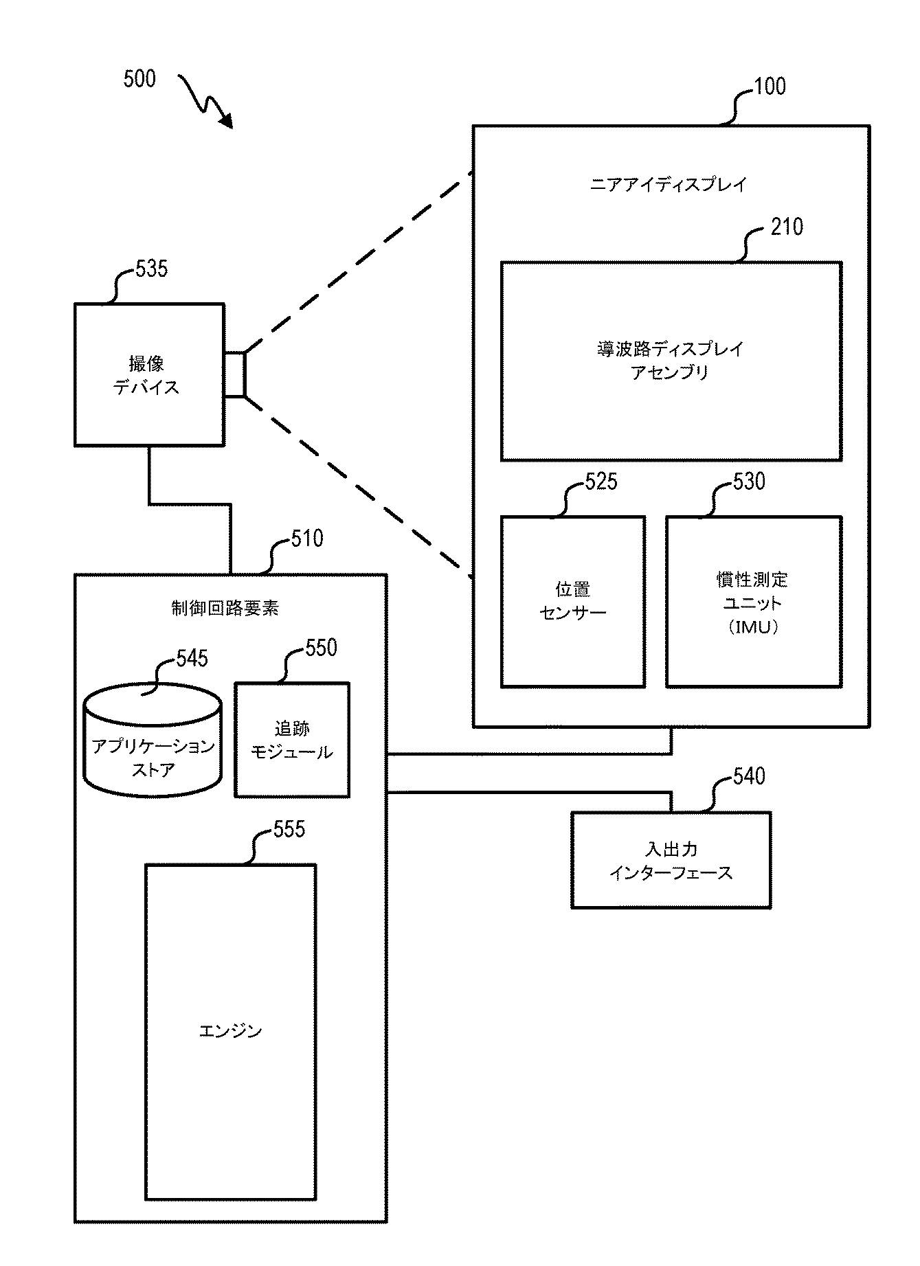
式7では、DNrawは、グローバル露光期間Texposure−globalから低減された露光期間Texposure−reducedから取得された、ピクセル1400のフォトダイオードからのPD ADCまたはFD ADCカウント出力を表す。(カウント値によって表される)電荷の量は露光期間に正比例するので、DNrawは、すべてのフォトダイオードからのカウント値が同じ露光期間に基づいて取得され、同じスケールに従うように、Texposure−globalとTexposure−reducedとの間の比に基づいて、正規化されたカウント値DNnormに外挿され得る。
In Equation 7, the DN raw represents the PD ADC or FD ADC count output from the
図14Aの例では、ピクセルセル1400のフォトダイオードは単一のADCを共有する。しかしながら、いくつかの例では、異なるピクセルセルのフォトダイオードが単一のADCを共有することができ、ピクセルセルのフォトダイオードのためのTTS動作は、異なるピクセルセルの別のフォトダイオードの露光期間を制御することができる。単一のADCを共有するフォトダイオードはカーネル中でグループ化され得、カーネルは、異なるピクセルセルからのまたは同じピクセルセルからのフォトダイオードを含むことができる。カーネル中のフォトダイオードの各グループは、同じまたは異なる光成分を検出するように構成され得る。カーネルのフォトダイオードのグループでは、マスタフォトダイオード(たとえば、第1のフォトダイオード)を除くフォトダイオードのすべてが、PD ADC動作および/またはFD ADC動作のみを実施するためにADCへのアクセスを有するが、第1のフォトダイオードは、TTS動作、ならびにPD ADC動作および/またはFD ADC動作を実施するためにADCへのアクセスを有する。グループ内のすべてのフォトダイオードは、マスタフォトダイオードの電荷検知ユニットが飽和されたときに停止され得る同じ露光期間を有することができる。その結果、PD ADC動作および/またはFD ADC動作に基づく、それらのフォトダイオードの電荷検知ユニットの量子化結果は、依然として、妥当な忠実度で光成分の強度を表すことができる。一方、マスタフォトダイオードからの飽和の指示がない場合、フォトダイオードは、低光強度および中光強度の測定についての最小信号対雑音比を維持するために、事前構成された露光期間内に少なくともしきい値量の電荷を生成することができ、これは、ダイナミックレンジの下限を設定し得る。
In the example of FIG. 14A, the photodiode in
カーネル中へのフォトダイオードのグループ化は、様々な方式に基づき得、用途固有であり得る。一例では、ピクセルのカーネルは、撮像されるべき所定の物体の輪郭/形状に基づいて画定され得る。図15A、図15B、および図15Cは、ターゲット物体の輪郭/形状に基づいて決定されたカーネルの例を示す。図15Aに示されているように、カーネルは、向きをもつ光源1500からの光の放射を反射する形状に基づく5つのピクセルセルを含むことができ、1つのピクセルセルが中心にあり、4つのピクセルセルが4つの側(たとえば、北、南、左、および右)にある。図15Aでは、1502、1504、1506および1508を含むピクセルセルの4つのカーネルが示されている。カーネル1502は、カーネル1502のマスタフォトダイオードを含むピクセルセル1502a、ならびにピクセルセル1502b、1502c、および1502dを含む。カーネル1504は、カーネル1504のマスタフォトダイオードを含むピクセルセル1504a、ならびにピクセルセル1504b、1504c、および1504dを含む。カーネル1506は、カーネル1506のマスタフォトダイオードを含むピクセルセル1506a、ならびにピクセルセル1506b、1506c、および1506dを含む。その上、カーネル1508は、カーネル1508のマスタフォトダイオードを含むピクセルセル1508a、ならびにピクセルセル1508b、1508c、および1508dを含む。
Grouping of photodiodes in the kernel can be based on various schemes and can be application specific. In one example, the pixel kernel can be defined based on the contour / shape of a given object to be imaged. 15A, 15B, and 15C show examples of kernels determined based on the contour / shape of the target object. As shown in FIG. 15A, the kernel can contain five pixel cells based on a shape that reflects the radiation of light from an oriented
図15Aに示されているカーネルでは、カーネルの中心にあるピクセルセルは、TTS動作が実施され得るマスタフォトダイオードを含むことができ、飽和が検出された場合、上記で説明されたように、カーネルのすべてのフォトダイオードの露光期間は低減され得る。たとえば、ピクセルセルアレイが、向きをもつ光源1500を撮像するために使用される場合、カーネルの中心にあるピクセルセルは、向きをもつ光源の最も明るい部分から光を受け取ることができ、電荷貯蔵デバイスを飽和させる。カーネル内のすべてのフォトダイオードについての露光期間は、飽和が検出されると停止され得、それにより、放射された光ならびにシーンの他の部分からの光を受け取り得る、カーネル内の他のピクセルセルは、飽和された出力ではなく、入射光に線形的に関係するデジタル出力を生成することができる。
In the kernel shown in FIG. 15A, the pixel cell at the center of the kernel can contain a master photodiode in which a TTS operation can be performed, and if saturation is detected, the kernel as described above. The exposure period of all photodiodes in can be reduced. For example, if a pixel cell array is used to image an oriented
カーネルの中心ピクセル中のフォトダイオードは、異なる光成分のためのマスタフォトダイオードとして構成され得る。各マスタフォトダイオードは、同じ光成分を検出する(カーネル内の)他のフォトダイオードとADCを共有することができ、他のフォトダイオードの露光期間を制御することができる。たとえば、図15Bおよび図15Cに示されているように、各ピクセルセル(たとえば、ピクセルセル1502c)は、可視単色光を検出するための2つのフォトダイオード(M)と、近赤外線を検出するためのフォトダイオード(NIR)と、緑色光を検出するためのフォトダイオード(G)とを含む。Mフォトダイオード、NIRフォトダイオード、およびGフォトダイオードの各セットはADCを共有し、したがって、各カーネルについて4つのADCが提供され、各カーネルは、中心ピクセルセル(たとえば、ピクセルセル1504a)中に2つのマスタMフォトダイオードと、マスタNIRフォトダイオードと、マスタGフォトダイオードとを有することができる。図15Bでは、(円によって示される)マスタMフォトダイオードは、同じカーネル中の他のMフォトダイオードの露光期間を制御することができ、図15Cでは、(円によって示される)マスタNIRフォトダイオードは、同じカーネル中の他のNIRフォトダイオードの露光期間を制御することができる。
The photodiode in the central pixel of the kernel can be configured as a master photodiode for different light components. Each master photodiode can share the ADC with other photodiodes (in the kernel) that detect the same light component and can control the exposure period of the other photodiodes. For example, as shown in FIGS. 15B and 15C, each pixel cell (eg,
別の例として、同様の強度の光成分を受け取る可能性があるピクセルセルがカーネルを形成することができる。ピクセルセルアレイ内のカーネルのフォトダイオードの空間分布は、画像センサーの用途に基づき得る。図16Aおよび図16Bは、ピクセルセルアレイ内のフォトダイオードの異なる空間分布を有するカーネルの例を示す。図16Aに示されているように、画像センサー1600は、シーンから(ドット1602a、ドット1602bなどを含む)パターン1602の構造化NIR光を受け取るように構成され得る。この用途では、カーネル1604は、パターン1602に基づいて離間されたピクセルセル(たとえば、1604a、1604b、1604c、および1604d)を含むことができ、カーネルのマスタピクセルセル(たとえば、1604a)が、カーネル内の他のピクセルセルのNIRフォトダイオードの露光期間を制御するためのNIRフォトダイオードを含む。
As another example, pixel cells that may receive light components of similar intensity can form the kernel. The spatial distribution of kernel photodiodes within a pixel array can be based on the application of the image sensor. 16A and 16B show examples of kernels with different spatial distributions of photodiodes within a pixel array. As shown in FIG. 16A, the
いくつかの例では、カーネルは、上記で説明されたように、同じピクセルセルのフォトダイオードをも含むことができる。そのような仕組みは、たとえば、画像センサーがシーンの小さい部分を撮像するために使用されるとき、および/または画像センサーが強い周辺光を伴う環境において動作するとき、ならびにピクセルセルの各フォトダイオードが高強度光成分を受け取ることができ、ピクセルセル内の各フォトダイオードの電荷検知ユニットが飽和する可能性がある場合、提供され得る。図16Bに示されているように、各ピクセルセルは、他のまたは同じ光成分(たとえば、NIR、B、Mなど)を検出する他のフォトダイオードの露光期間を制御することができる光成分(たとえば、円で囲まれている単色)を検出するためのマスタフォトダイオードを含むことができる。 In some examples, the kernel can also include photodiodes in the same pixel cell, as described above. Such a mechanism is, for example, when the image sensor is used to capture a small part of the scene and / or when the image sensor operates in an environment with strong ambient light, and each photodiode in a pixel cell. High intensity light components can be received and can be provided if the charge sensing unit of each photodiode in the pixel cell can be saturated. As shown in FIG. 16B, each pixel cell has a light component (eg, NIR, B, M, etc.) that can control the exposure period of other photodiodes that detect other or same light components (eg, NIR, B, M, etc.). For example, it can include a master photodiode to detect (a single color circled).
図17は、図14AのPD0およびPD1など、第1のフォトダイオードおよび第2のフォトダイオードを備える複数のフォトダイオードによって光強度測定を実施するための方法1700を示す。第1のフォトダイオードと第2のフォトダイオードとは、図14Aに示されているように、同じピクセルセル602aの一部であり得るか、または、図15A〜図16Bに示されているように、異なるピクセルセル中にあり得る。第1のフォトダイオードと第2のフォトダイオードとは、同じ波長範囲または異なる波長範囲の入射光成分を検出するように構成され得る。第1のフォトダイオードは、第1の電荷貯蔵デバイス(たとえば、電荷貯蔵デバイス902a)と第1の切替え可能バッファ(たとえば、バッファ904a)とを備える第1の電荷検知ユニット(たとえば、電荷検知ユニット614a)と結合され得、第2のフォトダイオードは、第2の電荷貯蔵デバイス(たとえば、電荷貯蔵デバイス902b)と第2の切替え可能バッファ(たとえば、バッファ904b)とを備える第2の電荷検知ユニット(たとえば、電荷検知ユニット614b)と結合され得る。第1の電荷検知ユニットの出力および第2の電荷検知ユニットの出力は、第1の切替え可能バッファがオンに切り替えられたとき、第1の電荷貯蔵デバイスにおいて第1の電圧を量子化することができ、第2の切替え可能バッファがオンに切り替えられたとき、第2の電荷貯蔵デバイスにおいて第2の電圧を量子化することができる単一のADC(たとえば、ADC616)と結合される。第1の電荷貯蔵デバイスと第2の電荷デバイスの両方が、1次キャパシタと補助キャパシタとを含むことができる。
FIG. 17
方法1700はステップ1702から開始し、第1のフォトダイオードが、第1の電荷を生成するために入射光に露光される。いくつかの例では、第1のシャッタースイッチが第1のフォトダイオードと電荷シンクとの間に結合され、第1のシャッタースイッチは、第1の電荷を生成するために第1のフォトダイオードを入射光に露光するためにオフに切り替えられ得、第1のシャッタースイッチをオフに切り替えることは、露光期間であることができる。
ステップ1704において、第2のフォトダイオードは、第2の電荷を生成するために入射光に露光される。いくつかの例では、第2のシャッタースイッチが第2のフォトダイオードと電荷シンクとの間に結合され、第2のシャッタースイッチは、第2の電荷を生成するために第2のフォトダイオードを入射光に露光するためにオフに切り替えられ得る。いくつかの例では、第1のシャッタースイッチと第2のシャッタースイッチとは、露光期間が第1のフォトダイオードと第2のフォトダイオードの両方について同じ時間において開始するように、同じ時間においてオフに切り替えられ得る。
In
ステップ1706において、第1の電荷検知ユニットは、第1の電荷を第1の電圧に変換することができる。いくつかの例では、第1の電荷検知ユニットは、第1の転送スイッチを介して第1のフォトダイオードと結合され、第1の転送スイッチは、第1のフォトダイオードが、ある量の第1の残留電荷を第1の電荷の一部として貯蔵し、第1の電荷の残りを第1のオーバーフロー電荷として第1の電荷検知ユニットの第1の電荷貯蔵デバイスに転送することを可能にするように、バイアスされ得る。第1のオーバーフロー電荷は、第1の電荷貯蔵デバイスの1次キャパシタと補助キャパシタの両方に貯蔵され得る。ステップ1706において、露光期間中の第1の電荷貯蔵デバイス中の第1のオーバーフロー電荷の蓄積に基づいて、第1の電圧を生じさせることができる。その上、第1の切替え可能バッファは、TTS動作を実施するために第1の電荷貯蔵デバイスをADCに接続するためにオンにされる。
In
ステップ1708において、第2の電荷検知ユニットは、第2の電荷を第1の電圧に変換することができる。いくつかの例では、第2の電荷検知ユニットは、第2の転送スイッチを介して第2のフォトダイオードと結合され、第2の転送スイッチは、第2のフォトダイオードが、ある量の第2の残留電荷を第2の電荷の一部として貯蔵し、第2の電荷の残りを第2のオーバーフロー電荷として第2の電荷検知ユニットの第2の電荷貯蔵デバイスに転送することを可能にするように、バイアスされ得る。第2のオーバーフロー電荷は、第2の電荷貯蔵デバイスの1次キャパシタと補助キャパシタの両方に貯蔵され得る。ステップ1708において、露光期間中の第2の電荷貯蔵デバイス中の第2のオーバーフロー電荷の蓄積に基づいて、第2の電圧を生じさせることができる。その上、第2の切替え可能バッファは、第2の電荷貯蔵デバイスをADCから切断するためにオフにされる。
In
ステップ1710において、TTS動作の一部として、ADCは、第1の電圧に基づいて、第1の電荷の量が飽和しきい値に達したことを検出し、第1の電荷の量が飽和しきい値に達したときの飽和時間を測定するように制御される。詳細には、ステップ1710において、ADCは、第1の電圧を、第1の電荷貯蔵デバイスの飽和限界を表す静的しきい値電圧と比較することができる。第1の電圧が静的しきい値を越える場合、ADCは、第1の電荷貯蔵デバイスに貯蔵された(第1のオーバーフロー電荷によって表される)第1の電荷の量が飽和限界に達したという飽和の指示を出力することができる。その指示(たとえば、図14AのVOUT信号)は、自走カウンタ(たとえば、カウンタ914)からのカウント値を記憶するようにメモリ(たとえば、メモリ912)を制御することができ、カウント値は、第1のフォトダイオードによって受け取られた入射光成分の強度を表すことができる。
In
ステップ1712において、第1のフォトダイオードおよび第2のフォトダイオードの露光は、第1の電荷の量が飽和しきい値に達したことを検出したことに基づいて停止される。詳細には、ステップ1710からの(および第1のフォトダイオードのTTS動作からの)飽和の指示は、第1のフォトダイオードと第2のフォトダイオードの両方についての露光期間を停止するために第1および第2のシャッタースイッチを有効化するために、それらのスイッチの制御信号を却下することができる。
In
いくつかの例では、露光が終了した後に、ADCは、PD ADC測定およびFD ADC測定を実施するように制御され得る。詳細には、露光が終了した後に、1次キャパシタは、それぞれ、第1および第2の電荷貯蔵デバイスの補助キャパシタにおいて第1のオーバーフロー電荷の一部および第2のオーバーフロー電荷の一部を保存するために、第1の電荷貯蔵デバイスと第2の電荷貯蔵デバイスの両方の補助キャパシタから切断され得る。PD ADC動作の一部として、第1の電荷検知ユニットの1次キャパシタがリセットされ得、次いで、第1の転送スイッチは、第1の残留電荷を第1のフォトダイオードから1次キャパシタに転送するように制御され得る。ADCは、上記で説明されたように、第1の残留電荷を量子化するために、第1の電荷検知ユニットの1次キャパシタにおける第1の電圧を第1のランピング電圧と比較することができる。第1のフォトダイオードが第1の残留電荷によって飽和されたかどうかの決定が、PD ADC動作中に行われる。FD ADC動作では、1次キャパシタと補助キャパシタとが、1次キャパシタと補助キャパシタとの間で第1のオーバーフロー電荷の一部分と第1の残留電荷とを再分配するために、再び一緒に接続され得る。ADCは、第1のオーバーフロー電荷と第1の残留電荷との組合せを量子化するために、1次キャパシタおよび補助キャパシタにおける第1の電圧を第2の電圧ランプと比較することができ、量子化結果は、第1のオーバーフロー電荷の量を測定するために後処理され得る。TTS動作、PD ADC動作、またはFD ADC動作のうちの1つの結果は、第1の電荷貯蔵デバイスが第1のオーバーフロー電荷によって飽和されたかどうかと、第1のフォトダイオードが第1の残留電荷によって飽和されたかどうかとに基づいて第1のフォトダイオードによって受け取られた入射光成分の強度を表すために提供され得る。 In some examples, after the exposure is finished, the ADC can be controlled to perform PD ADC measurements and FD ADC measurements. Specifically, after the exposure is complete, the primary capacitors store a portion of the first overflow charge and a portion of the second overflow charge in the auxiliary capacitors of the first and second charge storage devices, respectively. Therefore, it can be disconnected from both the auxiliary capacitors of the first charge storage device and the second charge storage device. As part of the PD ADC operation, the primary capacitor of the first charge sensing unit may be reset, then the first transfer switch transfers the first residual charge from the first photodiode to the primary capacitor. Can be controlled as such. The ADC can compare the first voltage in the primary capacitor of the first charge detection unit with the first ramping voltage in order to quantize the first residual charge, as described above. .. The determination of whether the first photodiode is saturated by the first residual charge is made during PD ADC operation. In the FD ADC operation, the primary capacitor and the auxiliary capacitor are reconnected together to redistribute a portion of the first overflow charge and the first residual charge between the primary capacitor and the auxiliary capacitor. obtain. The ADC can compare the first voltage in the primary and auxiliary capacitors with the second voltage lamp to quantize the combination of the first overflow charge and the first residual charge. The result can be post-processed to measure the amount of first overflow charge. One result of TTS operation, PD ADC operation, or FD ADC operation is whether the first charge storage device is saturated by the first overflow charge and the first photodiode by the first residual charge. It may be provided to represent the intensity of the incident light component received by the first photodiode based on whether it is saturated or not.
ステップ1714において、ADCは、第2の電圧に基づいて、露光期間が終了する前に第2のフォトダイオードによって生成された第2の電荷の量を測定するように制御され得る。第1のフォトダイオードのためのTTS動作、PD ADC動作およびFD ADC動作が完了した後に、ADCを第2の電荷貯蔵デバイスの出力に接続するために、第1の切替え可能バッファは無効化され得、第2の切替え可能バッファは有効化され得る。PD ADC動作と、その後のFD ADC動作とは、ステップ1712において説明されたのと同様に、第2の電荷貯蔵デバイス上で実施され得る。PD ADC動作またはFD ADC動作のうちの1つの結果は、第2のフォトダイオードが第2の残留電荷によって飽和されたかどうかに基づいて第2のフォトダイオードによって受け取られた入射光成分の強度を表すために提供され得る。
In
本明細書のいくつかの部分は、情報に関する動作のアルゴリズムおよび記号表現に関して本開示の例について説明する。これらのアルゴリズム説明および表現は、データ処理技術分野の当業者が、他の当業者に自身の仕事の本質を効果的に伝えるために通常使用される。これらの動作は、機能的に、計算量的に、または論理的に説明されるが、コンピュータプログラムまたは等価な電気回路、マイクロコードなどによって実装されることが理解される。さらに、一般性の喪失なしに、動作のこれらの仕組みをモジュールと呼ぶことが時々好都合であることも証明された。説明される動作およびそれらの関連するモジュールは、ソフトウェア、ファームウェア、および/またはハードウェアにおいて具現され得る。 Some parts of the specification describe examples of the present disclosure with respect to algorithms and symbolic representations of behavior with respect to information. These algorithm descriptions and representations are commonly used by those skilled in the art of data processing technology to effectively convey the essence of their work to others. These operations are described functionally, computationally, or logically, but are understood to be implemented by computer programs or equivalent electrical circuits, microcode, and the like. Furthermore, it has also proved sometimes convenient to call these mechanisms of operation modules, without loss of generality. The operations described and their associated modules may be embodied in software, firmware, and / or hardware.
説明されるステップ、動作、またはプロセスは、1つまたは複数のハードウェアまたはソフトウェアモジュールで、単独でまたは他のデバイスとの組合せで実施または実装され得る。いくつかの例では、ソフトウェアモジュールは、コンピュータプログラムコードを含んでいるコンピュータ可読媒体を備えるコンピュータプログラム製品で実装され、コンピュータプログラムコードは、説明されるステップ、動作、またはプロセスのいずれかまたはすべてを実施するためにコンピュータプロセッサによって実行され得る。 The steps, operations, or processes described may be performed or implemented on one or more hardware or software modules, alone or in combination with other devices. In some examples, the software module is implemented in a computer program product that has a computer-readable medium that contains the computer program code, and the computer program code performs any or all of the steps, actions, or processes described. Can be performed by a computer processor.
本開示の例はまた、説明される動作を実施するための装置に関し得る。本装置は、必要とされる目的のために特別に構築され得、および/あるいは、本装置は、コンピュータに記憶されたコンピュータプログラムによって選択的にアクティブ化または再構成される汎用コンピューティングデバイスを備え得る。そのようなコンピュータプログラムは、非一時的有形コンピュータ可読記憶媒体、または、コンピュータシステムバスに結合され得る、電子命令を記憶するのに好適な任意のタイプのメディアに記憶され得る。さらに、本明細書で言及される任意のコンピューティングシステムは、単一のプロセッサを含み得るか、または、増加された計算能力のために複数のプロセッサ設計を採用するアーキテクチャであり得る。 The examples of the present disclosure may also relate to devices for performing the described operations. The device may be specifically constructed for the required purpose, and / or the device comprises a general purpose computing device that is selectively activated or reconfigured by a computer program stored in the computer. obtain. Such computer programs may be stored on non-temporary tangible computer readable storage media, or any type of media suitable for storing electronic instructions that may be coupled to a computer system bus. Moreover, any computing system referred to herein can include a single processor or can be an architecture that employs multiple processor designs for increased computing power.
本開示の例はまた、本明細書で説明されるコンピューティングプロセスによって製造される製品に関し得る。そのような製品は、コンピューティングプロセスから生じる情報を備え得、その情報は、非一時的有形コンピュータ可読記憶媒体に記憶され、本明細書で説明されるコンピュータプログラム製品または他のデータ組合せの任意の例を含み得る。 The examples of the present disclosure may also relate to products manufactured by the computing processes described herein. Such products may comprise information arising from the computing process, which information is stored on non-temporary tangible computer readable storage media and is any computer program product or other data combination described herein. It may include an example.
本明細書で使用される言い回しは、主に読みやすさおよび教授の目的で選択されており、その言い回しは、本発明の主題を画定または制限するために選択されていないことがある。したがって、本開示の範囲はこの詳細な説明によって限定されるのではなく、むしろ、本明細書に基づく出願に関して生じる請求項によって限定されることが意図される。したがって、例の開示は、以下の特許請求の範囲に記載される本開示の範囲を例示するものであり、限定するものではない。
The wording used herein is chosen primarily for readability and teaching purposes, and the wording may not be chosen to define or limit the subject matter of the invention. Accordingly, the scope of this disclosure is not limited by this detailed description, but rather is intended to be limited by the claims arising in connection with the application under this specification. Therefore, the disclosure of the examples exemplifies, but is not limited to, the scope of the present disclosure described in the claims below.
Claims (20)
第2の電荷を生成するための第2のフォトダイオードと、
前記第1の電荷を第1の電圧に変換するための第1の電荷検知ユニットと、
前記第2の電荷を第2の電圧に変換するための第2の電荷検知ユニットと、
飽和時間と電荷の量とを測定することが可能なADCと、
コントローラと
を備える装置であって、前記コントローラは、
前記第1のフォトダイオードおよび前記第2のフォトダイオードを入射光に露光して、前記第1の電荷および前記第2の電荷をそれぞれ生成させることと、
前記第1の電圧に基づいて、前記第1の電荷の量が飽和しきい値に達したことを検出し、前記第1の電荷の前記量が前記飽和しきい値に達したときの前記飽和時間を測定するために、前記ADCを前記第1の電荷検知ユニットに接続することと、
前記第1の電荷の前記量が前記飽和しきい値に達したことを検出したことに基づいて、前記入射光への前記第1のフォトダイオードおよび前記第2のフォトダイオードの前記露光を停止することと、
前記第2の電圧に基づいて、前記露光が終了する前に前記第2のフォトダイオードによって生成された前記第2の電荷の量を測定するために、前記ADCを前記第2の電荷検知ユニットに接続することと
を行うように構成された、装置。 A first photodiode for generating a first charge, and
A second photodiode for generating a second charge, and
A first charge detection unit for converting the first charge into a first voltage, and
A second charge detection unit for converting the second charge into a second voltage, and
ADCs that can measure saturation time and amount of charge,
A device including a controller, wherein the controller is
Exposing the first photodiode and the second photodiode to incident light to generate the first charge and the second charge, respectively.
Based on the first voltage, it is detected that the amount of the first charge has reached the saturation threshold, and the saturation when the amount of the first charge reaches the saturation threshold. To connect the ADC to the first charge detection unit to measure the time,
Based on the detection that the amount of the first charge has reached the saturation threshold, the exposure of the first photodiode and the second photodiode to the incident light is stopped. That and
Based on the second voltage, the ADC is transferred to the second charge sensing unit to measure the amount of the second charge generated by the second photodiode before the end of the exposure. A device configured to connect and do.
前記第2のフォトダイオードと第2の電荷シンクとの間に結合された第2のシャッタースイッチと
をさらに備え、
前記コントローラが、
前記第1のシャッタースイッチおよび前記第2のシャッタースイッチを無効化することに基づいて、前記第1のフォトダイオードおよび前記第2のフォトダイオードを前記入射光に露光することと、
前記第1のシャッタースイッチおよび前記第2のシャッタースイッチを有効化することに基づいて、前記入射光への前記第1のフォトダイオードおよび前記第2のフォトダイオードの前記露光を停止することと
を行うように構成された、請求項1に記載の装置。 A first shutter switch coupled between the first photodiode and the first charge sink,
Further comprising a second shutter switch coupled between the second photodiode and the second charge sink.
The controller
Exposing the first photodiode and the second photodiode to the incident light based on disabling the first shutter switch and the second shutter switch.
Based on enabling the first shutter switch and the second shutter switch, the exposure of the first photodiode and the second photodiode to the incident light is stopped. The device according to claim 1, which is configured as described above.
前記装置が、
前記第1のフォトダイオードと前記第1の電荷検知ユニットとの間に結合された第1の転送スイッチと、
前記第2のフォトダイオードと前記第2の電荷検知ユニットとの間に結合された第2の転送スイッチと
をさらに備え、
前記コントローラが、
前記第1の電荷を前記第1の電荷検知ユニットの前記第1のキャパシタに転送するように前記第1の転送スイッチを制御することと、
前記第1の電荷を前記第1の電荷検知ユニットの前記第2のキャパシタに転送するように前記第2の転送スイッチを制御することと、
前記第1の電荷および前記第2の電荷の前記転送が完了した後に、前記入射光への前記第1のフォトダイオードおよび前記第2のフォトダイオードの前記露光を停止することと
を行うように構成された、請求項1に記載の装置。 Each of the first charge detection unit and the second charge detection unit includes a first capacitor and a second capacitor, respectively.
The device
A first transfer switch coupled between the first photodiode and the first charge detection unit,
Further comprising a second transfer switch coupled between the second photodiode and the second charge detection unit.
The controller
Controlling the first transfer switch to transfer the first charge to the first capacitor of the first charge detection unit.
Controlling the second transfer switch to transfer the first charge to the second capacitor of the first charge detection unit.
After the transfer of the first charge and the second charge is completed, the exposure of the first photodiode and the second photodiode to the incident light is stopped. The device according to claim 1.
第1の時間において、前記第1の電荷の第1のオーバーフロー電荷を貯蔵のために前記第1のフォトダイオードから前記第1の電荷検知ユニットに転送するために、第1のバイアス電圧において前記第1の転送スイッチをバイアスすることと、
前記第1の時間において、前記第2の電荷の第2のオーバーフロー電荷を貯蔵のために前記第2のフォトダイオードから前記第2の電荷検知ユニットに転送するために、前記第1のバイアス電圧において前記第2の転送スイッチをバイアスすることと、
第2の時間において、前記第1の電荷の第1の残留電荷を貯蔵のために前記第1のフォトダイオードから前記第1の電荷検知ユニットに転送するために、第2のバイアス電圧において前記第1の転送スイッチをバイアスすることと、
前記第2の時間において、前記第2の電荷の第2の残留電荷を貯蔵のために前記第2のフォトダイオードから前記第2の電荷検知ユニットに転送するために、前記第2のバイアス電圧において前記第2の転送スイッチをバイアスすることと
を行うように構成され、
前記入射光への前記第1のフォトダイオードおよび前記第2のフォトダイオードの前記露光は、前記第1の残留電荷の前記転送と前記第2の残留電荷の前記転送とが完了した後に停止される、
請求項4に記載の装置。 The controller
At the first bias voltage, the first overflow charge of the first charge is transferred from the first photodiode to the first charge detection unit for storage in the first time. Biasing the transfer switch of 1 and
At the first bias voltage, in the first time, to transfer the second overflow charge of the second charge from the second photodiode to the second charge sensing unit for storage. Biasing the second transfer switch and
In the second time, at the second bias voltage, the first residual charge of the first charge is transferred from the first photodiode to the first charge sensing unit for storage. Biasing the transfer switch of 1 and
At the second bias voltage, in the second time, to transfer the second residual charge of the second charge from the second photodiode to the second charge sensing unit for storage. It is configured to bias the second transfer switch and to do so.
The exposure of the first photodiode and the second photodiode to the incident light is stopped after the transfer of the first residual charge and the transfer of the second residual charge are completed. ,
The device according to claim 4.
前記第2の電荷検知ユニットが、前記第1のキャパシタと前記ADCとの間に結合された第2の切替え可能バッファを含み、
前記コントローラは、
前記第1の転送スイッチが前記第1のバイアス電圧においてバイアスされたとき、前記第1のオーバーフロー電荷の量が前記飽和しきい値を超えるかどうかを検出し、前記第1のオーバーフロー電荷の前記量が前記飽和しきい値に達したときの前記飽和時間を測定するように、前記ADCを制御するために、前記第1のスイッチバッファを有効化することと、
前記入射光への前記第1のフォトダイオードおよび前記第2のフォトダイオードの前記露光が停止した後に、
前記第2のキャパシタに貯蔵された前記第2の残留電荷の量を測定するように前記ADCを制御することと
を行うように構成された、請求項5に記載の装置。 The first charge sensing unit comprises a first switchable buffer coupled between the first capacitor and the ADC.
The second charge sensing unit comprises a second switchable buffer coupled between the first capacitor and the ADC.
The controller
When the first transfer switch is biased at the first bias voltage, it detects whether the amount of the first overflow charge exceeds the saturation threshold and the amount of the first overflow charge. To enable the first switch buffer to control the ADC so as to measure the saturation time when the saturation threshold is reached.
After the exposure of the first photodiode and the second photodiode to the incident light is stopped.
The apparatus of claim 5, wherein the ADC is configured to control the ADC so as to measure the amount of the second residual charge stored in the second capacitor.
前記ADCが、前記第1の電圧を、前記飽和しきい値を表す第1の静的しきい値電圧と比較することに基づいて、前記飽和時間を測定するように構成された、
請求項6に記載の装置。 The first capacitor produces the first voltage when the first overflow charge is transferred to the first capacitor.
The ADC is configured to measure the saturation time based on comparing the first voltage with a first static threshold voltage representing the saturation threshold.
The device according to claim 6.
前記第1の残留電荷の前記転送より前に、前記コントローラが、
前記第1の補助キャパシタを前記第1の主キャパシタから切断することと、
前記第1の主キャパシタをリセットすることと
を行うように構成され、
前記第1の残留電荷は、第3の電圧を生成するために、前記第1の主キャパシタがリセットされた後に前記第1の主キャパシタに転送され、
前記ADCが、前記第1の主キャパシタにおける前記第3の電圧を第1のランピングしきい値電圧と比較することに基づいて、前記第1の主キャパシタに貯蔵された前記第1の残留電荷の量を測定するように構成された、
請求項7に記載の装置。 The first capacitor includes a first main capacitor and a first auxiliary capacitor.
Prior to the transfer of the first residual charge, the controller
Cutting the first auxiliary capacitor from the first main capacitor,
It is configured to do the resetting of the first main capacitor.
The first residual charge is transferred to the first main capacitor after the first main capacitor is reset in order to generate a third voltage.
The ADC of the first residual charge stored in the first main capacitor based on comparing the third voltage in the first main capacitor with the first ramping threshold voltage. Configured to measure quantity,
The device according to claim 7.
第4の電圧を生成するために、前記第1のオーバーフロー電荷の一部分を貯蔵する前記第1の補助キャパシタを前記第1の主キャパシタと接続することと、
前記第4の電圧を第2のランピングしきい値電圧と比較することに基づいて前記第1のオーバーフロー電荷の量を測定することと
を行うように構成された、請求項8に記載の装置。 After the ADC measures the amount of the first residual charge,
To connect the first auxiliary capacitor, which stores a part of the first overflow charge, to the first main capacitor in order to generate a fourth voltage.
The apparatus of claim 8, wherein the fourth voltage is configured to measure the amount of the first overflow charge based on comparing it to a second ramping threshold voltage.
前記選択は、前記第1の電圧が前記第1の静的しきい値電圧を越えるかどうかに基づき、前記第3の電圧が、前記第1のフォトダイオードの貯蔵容量を表す第2の静的しきい値電圧を越えるかどうかに基づき、
前記コントローラが、前記第1のフォトダイオードによって受け取られた前記入射光の強度を表すために、前記選択された出力を提供するように構成された、
請求項9に記載の装置。 The controller is configured to select the output produced by the ADC based on one of the first voltage, the third voltage, or the fourth voltage.
The selection is based on whether the first voltage exceeds the first static threshold voltage, where the third voltage represents the storage capacity of the first photodiode. Based on whether the threshold voltage is exceeded
The controller is configured to provide the selected output to represent the intensity of the incident light received by the first photodiode.
The device according to claim 9.
前記第2の残留電荷の前記転送より前に、前記コントローラが、
前記第2の補助キャパシタを前記第2の主キャパシタから切断することと、
前記第2の主キャパシタをリセットすることと
を行うように構成され、
前記第2の残留電荷は、前記第2の電圧を生成するために、前記第2の主キャパシタがリセットされた後に前記第2の主キャパシタに転送され、
前記ADCが、前記第2の主キャパシタにおける前記第2の電圧を第1のランピングしきい値電圧と比較することに基づいて、前記第2の主キャパシタに貯蔵された前記第2の残留電荷の前記量を測定するように構成された、
請求項6に記載の装置。 The second capacitor includes a second main capacitor and a second auxiliary capacitor.
Prior to the transfer of the second residual charge, the controller
Cutting the second auxiliary capacitor from the second main capacitor,
It is configured to do the resetting of the second main capacitor.
The second residual charge is transferred to the second main capacitor after the second main capacitor is reset in order to generate the second voltage.
Based on the ADC comparing the second voltage in the second main capacitor with the first ramping threshold voltage, the second residual charge stored in the second main capacitor. Configured to measure the amount,
The device according to claim 6.
第3の電圧を生成するために、前記第2のオーバーフロー電荷の一部分を貯蔵する前記第2の補助キャパシタを前記第2の主キャパシタと接続することと、
前記第3の電圧を第2のランピングしきい値電圧と比較することに基づいて前記第2のオーバーフロー電荷の量を測定することと
を行うように構成された、請求項11に記載の装置。 After the ADC measures the amount of the second residual charge,
To connect the second auxiliary capacitor, which stores a part of the second overflow charge, to the second main capacitor in order to generate a third voltage.
11. The apparatus of claim 11, configured to measure the amount of the second overflow charge based on comparing the third voltage with the second ramping threshold voltage.
前記選択は、前記第2の電圧が、前記第2のフォトダイオードの貯蔵容量を表す静的しきい値電圧を越えるかどうかに基づき、
前記コントローラが、前記第2のフォトダイオードによって受け取られた前記入射光の強度を表すために、前記選択された出力を提供するように構成された、
請求項12に記載の装置。 The controller is configured to select an output generated by the ADC based on one of the second voltage or the third voltage.
The selection is based on whether the second voltage exceeds a static threshold voltage that represents the storage capacity of the second photodiode.
The controller is configured to provide the selected output to represent the intensity of the incident light received by the second photodiode.
The device according to claim 12.
前記第2のフォトダイオードが、第2の波長範囲を有する前記入射光の第2の成分を検出するように構成された、請求項1に記載の装置。 The first photodiode is configured to detect a first component of the incident light having a first wavelength range.
The apparatus according to claim 1, wherein the second photodiode is configured to detect a second component of the incident light having a second wavelength range.
前記第1のピクセルセルと前記第2のピクセルセルとが1つまたは複数のピクセルセルだけ離される、
請求項17に記載の装置。 The first pixel cell and the second pixel cell are part of a pixel cell array.
The first pixel cell and the second pixel cell are separated by one or more pixel cells.
The device according to claim 17.
第2の電荷を生成するために、第2のフォトダイオードを前記入射光に露光することと、
第1の電荷検知ユニットによって、前記第1の電荷を第1の電圧に変換することと、
第2の電荷検知ユニットによって、前記第2の電荷を第2の電圧に変換することと、
前記第1の電圧に基づいて、前記第1の電荷の量が飽和しきい値に達したことを検出し、前記第1の電荷の前記量が前記飽和しきい値に達したときの飽和時間を測定するように、ADCを制御することと、
前記第1の電荷の前記量が前記飽和しきい値に達したことを検出したことに基づいて、前記入射光への前記第1のフォトダイオードおよび前記第2のフォトダイオードの前記露光を停止することと、
前記第2の電圧に基づいて、前記露光が終了する前に前記第2のフォトダイオードによって生成された前記第2の電荷の量を測定するように、前記ADCを制御することと
を含む、方法。 Exposing the first photodiode to incident light to generate a first charge,
To expose the second photodiode to the incident light in order to generate a second charge,
The first charge detection unit converts the first charge into a first voltage.
The second charge detection unit converts the second charge into a second voltage.
Based on the first voltage, it is detected that the amount of the first charge has reached the saturation threshold, and the saturation time when the amount of the first charge reaches the saturation threshold. To control the ADC and to measure
Based on the detection that the amount of the first charge has reached the saturation threshold, the exposure of the first photodiode and the second photodiode to the incident light is stopped. That and
A method comprising controlling the ADC to measure the amount of the second charge generated by the second photodiode before the end of the exposure based on the second voltage. ..
前記第2の電荷が、第2の波長範囲を有する前記入射光の第2の成分を検出することに基づいて前記第2のフォトダイオードによって生成され、
前記第1の波長範囲と前記第2の波長範囲とが異なる、請求項19に記載の方法。
The first charge is generated by the first photodiode based on detecting the first component of the incident light having the first wavelength range.
The second charge is generated by the second photodiode based on detecting a second component of the incident light having a second wavelength range.
19. The method of claim 19, wherein the first wavelength range and the second wavelength range are different.
Applications Claiming Priority (5)
| Application Number | Priority Date | Filing Date | Title |
|---|---|---|---|
| US201862719953P | 2018-08-20 | 2018-08-20 | |
| US62/719,953 | 2018-08-20 | ||
| US16/544,136 | 2019-08-19 | ||
| US16/544,136 US10931884B2 (en) | 2018-08-20 | 2019-08-19 | Pixel sensor having adaptive exposure time |
| PCT/US2019/047156 WO2020041241A1 (en) | 2018-08-20 | 2019-08-20 | Pixel sensor having adaptive exposure time |
Publications (1)
| Publication Number | Publication Date |
|---|---|
| JP2021534603A true JP2021534603A (en) | 2021-12-09 |
Family
ID=69523631
Family Applications (1)
| Application Number | Title | Priority Date | Filing Date |
|---|---|---|---|
| JP2020569765A Pending JP2021534603A (en) | 2018-08-20 | 2019-08-20 | Pixel sensor with adaptive exposure time |
Country Status (5)
| Country | Link |
|---|---|
| US (2) | US10931884B2 (en) |
| JP (1) | JP2021534603A (en) |
| CN (1) | CN112585950B (en) |
| TW (1) | TWI815951B (en) |
| WO (1) | WO2020041241A1 (en) |
Families Citing this family (25)
| Publication number | Priority date | Publication date | Assignee | Title |
|---|---|---|---|---|
| US10686996B2 (en) | 2017-06-26 | 2020-06-16 | Facebook Technologies, Llc | Digital pixel with extended dynamic range |
| US10598546B2 (en) | 2017-08-17 | 2020-03-24 | Facebook Technologies, Llc | Detecting high intensity light in photo sensor |
| US11393867B2 (en) | 2017-12-06 | 2022-07-19 | Facebook Technologies, Llc | Multi-photodiode pixel cell |
| US11906353B2 (en) | 2018-06-11 | 2024-02-20 | Meta Platforms Technologies, Llc | Digital pixel with extended dynamic range |
| US11463636B2 (en) | 2018-06-27 | 2022-10-04 | Facebook Technologies, Llc | Pixel sensor having multiple photodiodes |
| US10897586B2 (en) | 2018-06-28 | 2021-01-19 | Facebook Technologies, Llc | Global shutter image sensor |
| US10848255B2 (en) * | 2018-07-10 | 2020-11-24 | FG Innovation Company Limited | Method and apparatus for reporting RSRP |
| US10931884B2 (en) | 2018-08-20 | 2021-02-23 | Facebook Technologies, Llc | Pixel sensor having adaptive exposure time |
| US11956413B2 (en) | 2018-08-27 | 2024-04-09 | Meta Platforms Technologies, Llc | Pixel sensor having multiple photodiodes and shared comparator |
| US11595602B2 (en) | 2018-11-05 | 2023-02-28 | Meta Platforms Technologies, Llc | Image sensor post processing |
| US11218660B1 (en) | 2019-03-26 | 2022-01-04 | Facebook Technologies, Llc | Pixel sensor having shared readout structure |
| US11943561B2 (en) | 2019-06-13 | 2024-03-26 | Meta Platforms Technologies, Llc | Non-linear quantization at pixel sensor |
| US11726186B2 (en) * | 2019-09-30 | 2023-08-15 | Zoox, Inc. | Pixel filtering using multiple exposures |
| US11841438B2 (en) | 2019-09-30 | 2023-12-12 | Zoox, Inc. | Power control of sensors using multiple exposures |
| US11936998B1 (en) | 2019-10-17 | 2024-03-19 | Meta Platforms Technologies, Llc | Digital pixel sensor having extended dynamic range |
| US11902685B1 (en) | 2020-04-28 | 2024-02-13 | Meta Platforms Technologies, Llc | Pixel sensor having hierarchical memory |
| US11910114B2 (en) | 2020-07-17 | 2024-02-20 | Meta Platforms Technologies, Llc | Multi-mode image sensor |
| CN114114518A (en) * | 2020-08-28 | 2022-03-01 | 中强光电股份有限公司 | Optical waveguide, method for manufacturing optical waveguide, and head-mounted display device |
| US11956560B2 (en) | 2020-10-09 | 2024-04-09 | Meta Platforms Technologies, Llc | Digital pixel sensor having reduced quantization operation |
| US12022218B2 (en) | 2020-12-29 | 2024-06-25 | Meta Platforms Technologies, Llc | Digital image sensor using a single-input comparator based quantizer |
| CN115118896B (en) * | 2021-03-23 | 2025-09-30 | 思特威(上海)电子科技股份有限公司 | A driving method for an image sensor used for rolling exposure and an image sensor |
| CN115373064A (en) | 2021-05-20 | 2022-11-22 | 中强光电股份有限公司 | Optical waveguide |
| JP2024010357A (en) * | 2022-07-12 | 2024-01-24 | ブリルニクス シンガポール プライベート リミテッド | Solid-state imaging device, driving method for solid-state imaging device, and electronic equipment |
| US12506362B2 (en) | 2024-05-21 | 2025-12-23 | Dell Products L.P. | Self-powered autonomous reconfigurable intelligent surfaces using wide radio frequency power range harvesting circuit |
| US12531601B2 (en) * | 2024-06-05 | 2026-01-20 | Dell Products L.P. | Autonomous reconfigurable intelligent surface using antennas and power-dependent switchable rectification mechanism |
Citations (6)
| Publication number | Priority date | Publication date | Assignee | Title |
|---|---|---|---|---|
| JP2002314875A (en) * | 2001-01-29 | 2002-10-25 | Konica Corp | Photographing apparatus and image pickup device |
| JP2005328493A (en) * | 2004-04-12 | 2005-11-24 | Shigetoshi Sugawa | Solid-state imaging device, optical sensor, and operation method of solid-state imaging device |
| JP2010283525A (en) * | 2009-06-03 | 2010-12-16 | Toshiba Corp | Imaging device |
| US20120068051A1 (en) * | 2010-09-17 | 2012-03-22 | Samsung Electronics Co., Ltd. | Method Of Driving An Image Sensor |
| JP2015103998A (en) * | 2013-11-26 | 2015-06-04 | 株式会社ニコン | Imaging device and imaging device |
| JP2017227686A (en) * | 2016-06-20 | 2017-12-28 | リコーイメージング株式会社 | Focus detection device |
Family Cites Families (391)
| Publication number | Priority date | Publication date | Assignee | Title |
|---|---|---|---|---|
| US4596977A (en) | 1984-12-03 | 1986-06-24 | Honeywell Inc. | Dual slope analog to digital converter with out-of-range reset |
| US5053771A (en) | 1990-07-16 | 1991-10-01 | Eastman Kodak Company | Adaptive dual range analog to digital converter |
| JP2953297B2 (en) | 1994-03-30 | 1999-09-27 | 日本電気株式会社 | Light receiving element and driving method thereof |
| US5963369A (en) | 1996-06-03 | 1999-10-05 | Steinthal; Gregory | Digital solid-state binoculars |
| US5844512A (en) | 1997-07-28 | 1998-12-01 | Hewlett-Packard Company | Autoranging apparatus and method for improved dynamic ranging in analog to digital converters |
| US6057586A (en) * | 1997-09-26 | 2000-05-02 | Intel Corporation | Method and apparatus for employing a light shield to modulate pixel color responsivity |
| US6529241B1 (en) | 1998-02-27 | 2003-03-04 | Intel Corporation | Photodetecting device supporting saturation detection and electronic shutter |
| JP4178608B2 (en) | 1998-04-16 | 2008-11-12 | 株式会社ニコン | Solid-state imaging device |
| US6522395B1 (en) | 1999-04-30 | 2003-02-18 | Canesta, Inc. | Noise reduction techniques suitable for three-dimensional information acquirable with CMOS-compatible image sensor ICS |
| US6486504B1 (en) | 1999-10-26 | 2002-11-26 | Eastman Kodak Company | CMOS image sensor with extended dynamic range |
| US6545624B2 (en) | 2000-02-11 | 2003-04-08 | Hyundai Electronics Industries Co., Ltd. | Image sensor with analog-to-digital converter that generates a variable slope ramp signal |
| JP4518616B2 (en) | 2000-04-13 | 2010-08-04 | ソニー株式会社 | Solid-state imaging device, driving method thereof, and camera system |
| US20010040632A1 (en) * | 2000-05-09 | 2001-11-15 | Yang David Xiao Dong | Multiple sampling via a time-indexed method to achieve wide dynamic ranges |
| US6384905B1 (en) | 2000-07-07 | 2002-05-07 | The United States Of America As Represented By The Secretary Of The Navy | Optic flow sensor with fused elementary motion detector outputs |
| JP3984808B2 (en) | 2000-09-07 | 2007-10-03 | キヤノン株式会社 | Signal processing apparatus, imaging apparatus using the same, and radiation imaging system |
| US7079178B2 (en) | 2001-02-20 | 2006-07-18 | Jaroslav Hynecek | High dynamic range active pixel CMOS image sensor and data processing system incorporating adaptive pixel reset |
| JP2002330349A (en) | 2001-04-26 | 2002-11-15 | Fujitsu Ltd | XY address type solid-state imaging device |
| US6642503B2 (en) | 2001-06-13 | 2003-11-04 | Texas Instruments Incorporated | Time domain sensing technique and system architecture for image sensor |
| JP4949573B2 (en) | 2001-07-13 | 2012-06-13 | 浜松ホトニクス株式会社 | Photodetector |
| US9149175B2 (en) * | 2001-07-26 | 2015-10-06 | Given Imaging Ltd. | Apparatus and method for light control in an in-vivo imaging device |
| US20030049925A1 (en) | 2001-09-10 | 2003-03-13 | Layman Paul Arthur | High-density inter-die interconnect structure |
| CA2474560C (en) | 2002-02-01 | 2012-03-20 | Picometrix, Inc. | Planar avalanche photodiode |
| US6963369B1 (en) | 2002-04-01 | 2005-11-08 | Pixim, Inc. | Method for capturing and storing image information for multiple sampling operations in a digital pixel sensor |
| US7038820B1 (en) * | 2002-04-03 | 2006-05-02 | Eastman Kodak Company | Automatic exposure control for an image sensor |
| JP4175828B2 (en) | 2002-04-18 | 2008-11-05 | 抱 石井 | Imaging camera apparatus and imager image data reading method |
| US7362365B1 (en) | 2002-06-26 | 2008-04-22 | Pixim, Inc. | Digital image capture having an ultra-high dynamic range |
| JP3792628B2 (en) | 2002-09-02 | 2006-07-05 | 富士通株式会社 | Solid-state imaging device and image reading method |
| CN1234234C (en) | 2002-09-30 | 2005-12-28 | 松下电器产业株式会社 | Solid-state photographic device and equipment using the photographic device |
| DE60333410D1 (en) | 2003-01-10 | 2010-08-26 | Scherrer Inst Paul | Image pickup device for photon counting |
| US7280143B2 (en) | 2003-04-14 | 2007-10-09 | Micron Technology, Inc. | CMOS image sensor with active reset and 4-transistor pixels |
| US7456879B2 (en) | 2003-08-29 | 2008-11-25 | Aptina Imaging Corporation | Digital correlated double sampling using dual analog path |
| US6885331B2 (en) | 2003-09-15 | 2005-04-26 | Micron Technology, Inc. | Ramp generation with capacitors |
| DE60333757D1 (en) | 2003-11-04 | 2010-09-23 | St Microelectronics Res & Dev | Improvements in or relating to image sensors |
| FR2862448B1 (en) | 2003-11-14 | 2006-12-29 | St Microelectronics Sa | TENSION RAMP GENERATOR WITH SLOPE SUPPORT |
| KR100574959B1 (en) | 2003-11-24 | 2006-04-28 | 삼성전자주식회사 | CMOS image sensor with automatic exposure control |
| US6864817B1 (en) | 2003-12-30 | 2005-03-08 | Freescale Semiconductor, Inc. | Signaling dependent adaptive analog-to-digital converter (ADC) system and method of using same |
| US7129883B2 (en) | 2004-02-23 | 2006-10-31 | Sony Corporation | Method and apparatus for AD conversion, semiconductor device for detecting distribution of physical quantity, and electronic apparatus |
| WO2005083790A1 (en) | 2004-02-27 | 2005-09-09 | Texas Instruments Japan Limited | Solid-state imagine device, line sensor, optical sensor, and method for operating solid-state imaging device |
| CN1914915A (en) | 2004-04-23 | 2007-02-14 | 住友电气工业株式会社 | Encoding method and decoding method of moving picture data, terminal device implementing these methods, and two-way interactive system |
| GB0412296D0 (en) | 2004-06-02 | 2004-07-07 | Council Cent Lab Res Councils | Imaging device |
| US7508431B2 (en) | 2004-06-17 | 2009-03-24 | Hoya Corporation | Solid state imaging device |
| GB0416496D0 (en) | 2004-07-23 | 2004-08-25 | Council Of The Central Lab Of | Imaging device |
| JP4349232B2 (en) | 2004-07-30 | 2009-10-21 | ソニー株式会社 | Semiconductor module and MOS solid-state imaging device |
| BRPI0514555A (en) | 2004-08-23 | 2008-06-17 | Sony Corp | imaging apparatus, image signal processing method, and integrated circuit |
| US8144227B2 (en) | 2004-09-02 | 2012-03-27 | Sony Corporation | Image pickup device and image pickup result outputting method |
| WO2006073176A1 (en) | 2005-01-06 | 2006-07-13 | Nec Corporation | Semiconductor integrated circuit device |
| US7518645B2 (en) | 2005-01-06 | 2009-04-14 | Goodrich Corp. | CMOS active pixel sensor with improved dynamic range and method of operation |
| JP4459064B2 (en) | 2005-01-14 | 2010-04-28 | キヤノン株式会社 | Solid-state imaging device, control method thereof, and camera |
| JP2006197393A (en) | 2005-01-14 | 2006-07-27 | Canon Inc | Solid-state imaging device, camera, and driving method of solid-state imaging device |
| JP4589131B2 (en) | 2005-01-24 | 2010-12-01 | 株式会社フォトロン | Image sensor and image reading method thereof |
| GB2424781B (en) | 2005-03-30 | 2007-11-28 | Micron Technology Inc | High density row ram for column parallel CMOS image sensors |
| WO2006124592A2 (en) | 2005-05-12 | 2006-11-23 | California Institute Of Technology | Linear dynamic range enhancement in a cmos imager |
| TW201101476A (en) | 2005-06-02 | 2011-01-01 | Sony Corp | Semiconductor image sensor module and method of manufacturing the same |
| US20070013983A1 (en) | 2005-07-04 | 2007-01-18 | Dai Nippon Printing Co., Ltd. | Holographic viewing device, and holographic viewing card incorporating it |
| US7522341B2 (en) | 2005-07-12 | 2009-04-21 | Micron Technology, Inc. | Sharing of microlenses among pixels in image sensors |
| US20090040364A1 (en) | 2005-08-08 | 2009-02-12 | Joseph Rubner | Adaptive Exposure Control |
| US7636115B2 (en) * | 2005-08-11 | 2009-12-22 | Aptina Imaging Corporation | High dynamic range imaging device using multiple pixel cells |
| JP2007074447A (en) | 2005-09-07 | 2007-03-22 | Fujitsu Ltd | CMOS sensor |
| KR100775058B1 (en) | 2005-09-29 | 2007-11-08 | 삼성전자주식회사 | An image processing system including a pixel, an image sensor using the same, and the image sensor |
| US7608823B2 (en) | 2005-10-03 | 2009-10-27 | Teledyne Scientific & Imaging, Llc | Multimode focal plane array with electrically isolated commons for independent sub-array biasing |
| US7659925B2 (en) | 2005-10-04 | 2010-02-09 | Alexander Krymski | High speed CMOS image sensor circuits with memory readout |
| US7546026B2 (en) | 2005-10-25 | 2009-06-09 | Zoran Corporation | Camera exposure optimization techniques that take camera and scene motion into account |
| US7652313B2 (en) | 2005-11-10 | 2010-01-26 | International Business Machines Corporation | Deep trench contact and isolation of buried photodetectors |
| EP1874043B1 (en) | 2006-02-20 | 2013-12-04 | Panasonic Corporation | Image pick up apparatus |
| EP1830195A1 (en) | 2006-03-02 | 2007-09-05 | Dialog Semiconductor GmbH | Probeless DC testing of CMOS I/O circuits |
| JP4819561B2 (en) | 2006-04-24 | 2011-11-24 | 浜松ホトニクス株式会社 | Solid-state imaging device |
| JP4827627B2 (en) | 2006-06-16 | 2011-11-30 | キヤノン株式会社 | Imaging apparatus and processing method thereof |
| US7326903B2 (en) * | 2006-06-29 | 2008-02-05 | Noble Peak Vision Corp. | Mixed analog and digital pixel for high dynamic range readout |
| EP1881609A1 (en) | 2006-07-21 | 2008-01-23 | STMicroelectronics (Research & Development) Limited | Analogue to digital convertor having a non-linear ramp voltage |
| JP4289377B2 (en) | 2006-08-21 | 2009-07-01 | ソニー株式会社 | Physical quantity detection device and imaging device |
| JP4855192B2 (en) | 2006-09-14 | 2012-01-18 | 富士フイルム株式会社 | Image sensor and digital camera |
| US7361989B1 (en) | 2006-09-26 | 2008-04-22 | International Business Machines Corporation | Stacked imager package |
| JP2008228232A (en) | 2007-03-15 | 2008-09-25 | Canon Inc | Imaging apparatus, imaging method, program, and storage medium |
| US8107751B2 (en) | 2007-03-16 | 2012-01-31 | Sharp Laboratories Of America, Inc. | DPCM with adaptive range and PCM escape mode |
| US7839703B2 (en) | 2007-06-15 | 2010-11-23 | Micron Technology, Inc. | Subtraction circuits and digital-to-analog converters for semiconductor devices |
| US7825966B2 (en) | 2007-06-29 | 2010-11-02 | Omnivision Technologies, Inc. | High dynamic range sensor with blooming drain |
| JP5067850B2 (en) | 2007-08-02 | 2012-11-07 | キヤノン株式会社 | System, head-mounted display device, and control method thereof |
| US7956914B2 (en) | 2007-08-07 | 2011-06-07 | Micron Technology, Inc. | Imager methods, apparatuses, and systems providing a skip mode with a wide dynamic range operation |
| US20090066820A1 (en) | 2007-09-06 | 2009-03-12 | Broadcom Corporation | Filtering optimization via implicit bayer grid subsampling |
| US7940311B2 (en) | 2007-10-03 | 2011-05-10 | Nokia Corporation | Multi-exposure pattern for enhancing dynamic range of images |
| US8426793B1 (en) * | 2007-10-04 | 2013-04-23 | Geoffrey L. Barrows | Vision sensor |
| EP2063630A1 (en) | 2007-11-26 | 2009-05-27 | Thomson Licensing | Video capture device with variable shutter integration time |
| US8369458B2 (en) | 2007-12-20 | 2013-02-05 | Ralink Technology Corporation | Wireless receiving system with an adaptively configurable analog to digital converter |
| WO2009111556A1 (en) | 2008-03-04 | 2009-09-11 | Mesa Imaging Ag | Drift field demodulation pixel with pinned photo diode |
| EP2104234B1 (en) | 2008-03-21 | 2011-08-31 | STMicroelectronics Limited | Analog-to-digital conversion in image sensors |
| US8098955B2 (en) | 2008-03-25 | 2012-01-17 | Point Grey Research Inc. | Efficient selection and application of regions of interest in digital imaging |
| JP5269456B2 (en) | 2008-03-26 | 2013-08-21 | 株式会社東芝 | Image sensor and driving method thereof |
| US8089035B2 (en) * | 2008-04-16 | 2012-01-03 | Tower Semiconductor Ltd. | CMOS image sensor with high sensitivity wide dynamic range pixel for high resolution applications |
| EP2133918B1 (en) | 2008-06-09 | 2015-01-28 | Sony Corporation | Solid-state imaging device, drive method thereof and electronic apparatus |
| JP4661912B2 (en) | 2008-07-18 | 2011-03-30 | ソニー株式会社 | Solid-state imaging device and camera system |
| US20130218728A1 (en) | 2008-08-10 | 2013-08-22 | Rick Dan Hashop | Virtual on-line pre-shopping system and method |
| US7795650B2 (en) * | 2008-12-09 | 2010-09-14 | Teledyne Scientific & Imaging Llc | Method and apparatus for backside illuminated image sensors using capacitively coupled readout integrated circuits |
| US8625012B2 (en) | 2009-02-05 | 2014-01-07 | The Hong Kong University Of Science And Technology | Apparatus and method for improving dynamic range and linearity of CMOS image sensor |
| JP5400406B2 (en) | 2009-02-06 | 2014-01-29 | キヤノン株式会社 | Imaging device |
| KR101575851B1 (en) | 2009-03-13 | 2015-12-10 | 삼성전자주식회사 | Nonvolatile memory device and its programming method |
| EP2234387B8 (en) | 2009-03-24 | 2012-05-23 | Sony Corporation | Solid-state imaging device, driving method of solid-state imaging device, and electronic apparatus |
| JP5359465B2 (en) | 2009-03-31 | 2013-12-04 | ソニー株式会社 | Solid-state imaging device, signal processing method for solid-state imaging device, and imaging device |
| JP5306269B2 (en) | 2009-06-25 | 2013-10-02 | キヤノン株式会社 | Imaging apparatus and imaging method using optical coherence tomography |
| US8569807B2 (en) | 2009-09-01 | 2013-10-29 | Taiwan Semiconductor Manufacturing Company, Ltd. | Backside illuminated image sensor having capacitor on pixel region |
| JP5330520B2 (en) | 2009-09-11 | 2013-10-30 | パナソニック株式会社 | Analog / digital converter, image sensor system, camera device |
| KR101727270B1 (en) | 2009-11-06 | 2017-04-17 | 삼성전자주식회사 | Image sensor |
| US8384800B2 (en) | 2009-11-23 | 2013-02-26 | Samsung Electronics Co., Ltd. | Methods of acquiring images |
| KR101111946B1 (en) | 2009-12-17 | 2012-02-14 | 엠텍비젼 주식회사 | Image sharing device, image signal processor chip and memory sharing method between chips |
| US8405017B2 (en) | 2009-12-24 | 2013-03-26 | Imagerlabs Inc. | Adjustable CMOS sensor array |
| EP2533521A4 (en) | 2010-02-05 | 2014-09-10 | Konica Minolta Advanced Layers | SEMICONDUCTOR IMAGE CAPTURE DEVICE |
| US20150309316A1 (en) | 2011-04-06 | 2015-10-29 | Microsoft Technology Licensing, Llc | Ar glasses with predictive control of external device based on event input |
| US20120200499A1 (en) | 2010-02-28 | 2012-08-09 | Osterhout Group, Inc. | Ar glasses with event, sensor, and user action based control of applications resident on external devices with feedback |
| JP2011229120A (en) | 2010-03-30 | 2011-11-10 | Sony Corp | Solid-state imaging device, signal processing method of solid-state imaging device, and electronic apparatus |
| JP2011216966A (en) | 2010-03-31 | 2011-10-27 | Sony Corp | Solid-state imaging element, and method of driving the same, and electronic equipment |
| JP2011258728A (en) | 2010-06-08 | 2011-12-22 | Sharp Corp | Solid state image sensor and electronic information apparatus |
| JP5554644B2 (en) | 2010-06-29 | 2014-07-23 | パナソニック株式会社 | Solid-state imaging device |
| US20120016817A1 (en) | 2010-07-19 | 2012-01-19 | Smith S Alex | Predicting Life Changes of Members of a Social Networking System |
| US8606051B2 (en) | 2010-08-16 | 2013-12-10 | SK Hynix Inc. | Frame-wise calibration of column-parallel ADCs for image sensor array applications |
| US8866945B2 (en) | 2010-09-26 | 2014-10-21 | Hiok Nam Tay | Color image sampling and reconstruction |
| CN103119928B (en) | 2010-09-30 | 2016-05-25 | 佳能株式会社 | Solid state image pickup device |
| US8773577B2 (en) | 2010-10-27 | 2014-07-08 | Qualcomm Incorporated | Region of interest extraction |
| US8698843B2 (en) | 2010-11-02 | 2014-04-15 | Google Inc. | Range of focus in an augmented reality application |
| US20120113119A1 (en) | 2010-11-05 | 2012-05-10 | Nova Research, Inc. | Super resolution infrared imaging system |
| JP5664141B2 (en) | 2010-11-08 | 2015-02-04 | ソニー株式会社 | Solid-state imaging device and camera system |
| US8576276B2 (en) | 2010-11-18 | 2013-11-05 | Microsoft Corporation | Head-mounted display device which provides surround video |
| KR101710481B1 (en) | 2010-11-29 | 2017-02-28 | 삼성전자주식회사 | CDS circuit, method thereof and devices having the same |
| TWI462265B (en) | 2010-11-30 | 2014-11-21 | 財團法人工業技術研究院 | Image capture device |
| KR101754131B1 (en) | 2010-12-01 | 2017-07-06 | 삼성전자주식회사 | Sampling circuit, sampling method, and photo detecting apparatus |
| US8294077B2 (en) | 2010-12-17 | 2012-10-23 | Omnivision Technologies, Inc. | Image sensor having supplemental capacitive coupling node |
| US8847136B2 (en) | 2011-01-02 | 2014-09-30 | Pixim, Inc. | Conversion gain modulation using charge sharing pixel |
| US8717467B2 (en) | 2011-01-25 | 2014-05-06 | Aptina Imaging Corporation | Imaging systems with array cameras for depth sensing |
| US8587501B2 (en) | 2011-02-17 | 2013-11-19 | Global Oled Technology Llc | Electroluminescent display device with optically communicating chiplets |
| US8674282B2 (en) | 2011-03-25 | 2014-03-18 | Aptina Imaging Corporation | Pumped pinned photodiode pixel array |
| TWI456990B (en) | 2011-04-08 | 2014-10-11 | 原相科技股份有限公司 | High dynamic range image sensing circuit and high dynamic range image reading method |
| KR101251744B1 (en) | 2011-04-13 | 2013-04-05 | 엘지이노텍 주식회사 | Wdr pixel array, image sensor including the pixel array and method for operating the same |
| KR101241704B1 (en) | 2011-04-14 | 2013-03-19 | 엘지이노텍 주식회사 | Pixel, pixel array, image sensor including the same and method for operating the image sensor |
| US8637800B2 (en) | 2011-04-19 | 2014-01-28 | Altasens, Inc. | Image sensor with hybrid heterostructure |
| US8575531B2 (en) | 2011-04-26 | 2013-11-05 | Aptina Imaging Corporation | Image sensor array for back side illumination with global shutter using a junction gate photodiode |
| US9093579B2 (en) | 2011-04-28 | 2015-07-28 | Semiconductor Components Industries, Llc | Dielectric barriers for pixel arrays |
| JP5808162B2 (en) | 2011-06-23 | 2015-11-10 | キヤノン株式会社 | Imaging device, imaging apparatus, and driving method of imaging device |
| US20190331914A1 (en) | 2011-07-20 | 2019-10-31 | Google Llc | Experience Sharing with Region-Of-Interest Selection |
| JP5868065B2 (en) | 2011-08-05 | 2016-02-24 | キヤノン株式会社 | Imaging device |
| JP5901186B2 (en) | 2011-09-05 | 2016-04-06 | キヤノン株式会社 | Solid-state imaging device and driving method thereof |
| US20130056809A1 (en) | 2011-09-07 | 2013-03-07 | Duli Mao | Image Sensor with Reduced Noiseby Blocking Nitridation Over Selected Areas |
| US8223024B1 (en) | 2011-09-21 | 2012-07-17 | Google Inc. | Locking mechanism based on unnatural movement of head-mounted display |
| US8890047B2 (en) | 2011-09-21 | 2014-11-18 | Aptina Imaging Corporation | Stacked-chip imaging systems |
| US8461660B2 (en) | 2011-09-30 | 2013-06-11 | Omnivision Technologies, Inc. | CMOS image sensor with reset shield line |
| GB201117319D0 (en) | 2011-10-06 | 2011-11-16 | Isis Innovation | Active pixel image sensor |
| JP2013084785A (en) | 2011-10-11 | 2013-05-09 | Sony Corp | Solid-state imaging device, and imaging device |
| JP2013090127A (en) | 2011-10-18 | 2013-05-13 | Olympus Corp | Solid-state imaging apparatus and imaging apparatus |
| US8804021B2 (en) | 2011-11-03 | 2014-08-12 | Omnivision Technologies, Inc. | Method, apparatus and system for providing improved full well capacity in an image sensor pixel |
| WO2013070942A1 (en) * | 2011-11-08 | 2013-05-16 | Rambus Inc. | Image sensor sampled at non-uniform intervals |
| US10598929B2 (en) | 2011-11-09 | 2020-03-24 | Google Llc | Measurement method and system |
| JP5802520B2 (en) | 2011-11-11 | 2015-10-28 | 株式会社 日立産業制御ソリューションズ | Imaging device |
| JP5963421B2 (en) | 2011-11-17 | 2016-08-03 | オリンパス株式会社 | Solid-state imaging device and imaging device |
| KR20130062188A (en) | 2011-12-02 | 2013-06-12 | 삼성전자주식회사 | Image sensor, and image processing device including the same |
| JP6051516B2 (en) | 2011-12-07 | 2016-12-27 | セイコーエプソン株式会社 | Imaging apparatus and imaging method |
| KR101801339B1 (en) | 2011-12-07 | 2017-11-27 | 한국전자통신연구원 | Fast frequency comparator with wide dynamic range |
| US8754798B2 (en) | 2011-12-21 | 2014-06-17 | Realtek Semiconductor Corp. | High-speed successive-approximation-register analog-to-digital converter and method thereof |
| US20130180841A1 (en) | 2012-01-17 | 2013-07-18 | Esat Yilmaz | Sensor Stack with Opposing Electrodes |
| US8735795B2 (en) | 2012-01-20 | 2014-05-27 | Omnivision Technologies, Inc. | Image sensor with integrated ambient light detection |
| US9531990B1 (en) | 2012-01-21 | 2016-12-27 | Google Inc. | Compound prediction using multiple sources or prediction modes |
| JP6141584B2 (en) | 2012-01-24 | 2017-06-07 | アリゾナ ボード オブ リージェンツ オン ビハーフ オブ ザ ユニバーシティ オブ アリゾナ | Compact line-of-sight head-mounted display |
| CN103258829A (en) | 2012-02-16 | 2013-08-21 | 索尼公司 | Solid-state imaging device, image sensor, method of manufacturing image sensor, and electronic apparatus |
| JP6004664B2 (en) | 2012-02-17 | 2016-10-12 | キヤノン株式会社 | Photoelectric conversion device and method for driving photoelectric conversion device |
| US8742311B2 (en) | 2012-02-27 | 2014-06-03 | Omnivision Technologies, Inc. | Enhanced pixel cell architecture for an image sensor having a direct output from a buried channel source follower transistor to a bit line |
| JP6164846B2 (en) | 2012-03-01 | 2017-07-19 | キヤノン株式会社 | Imaging device, imaging system, and driving method of imaging device |
| JP5965674B2 (en) | 2012-03-05 | 2016-08-10 | オリンパス株式会社 | Solid-state imaging device and imaging device |
| US8569700B2 (en) | 2012-03-06 | 2013-10-29 | Omnivision Technologies, Inc. | Image sensor for two-dimensional and three-dimensional image capture |
| TW201340708A (en) | 2012-03-19 | 2013-10-01 | 新力股份有限公司 | Solid-state imaging device and electronic device |
| KR101930755B1 (en) | 2012-03-21 | 2018-12-19 | 삼성전자주식회사 | Method of driving an image sensor |
| JP6402624B2 (en) | 2012-03-30 | 2018-10-10 | 株式会社ニコン | Imaging device and imaging apparatus |
| US8957358B2 (en) | 2012-04-27 | 2015-02-17 | Taiwan Semiconductor Manufacturing Company, Ltd. | CMOS image sensor chips with stacked scheme and methods for forming the same |
| US9270906B2 (en) | 2012-05-02 | 2016-02-23 | Semiconductor Components Industries, Llc | Exposure time selection using stacked-chip image sensors |
| US8963759B2 (en) | 2012-05-03 | 2015-02-24 | Semiconductor Components Industries, Llc | Imaging systems with per-column analog-to-digital converter non-linearity correction capabilities |
| US8779346B2 (en) | 2012-05-14 | 2014-07-15 | BAE Systems Imaging Solutions Inc. | Digital pixel sensor with reduced noise |
| JP5885608B2 (en) | 2012-07-23 | 2016-03-15 | 株式会社東芝 | Solid-state imaging device |
| JP6071315B2 (en) | 2012-08-08 | 2017-02-01 | オリンパス株式会社 | Solid-state imaging device and imaging device |
| US9531961B2 (en) | 2015-05-01 | 2016-12-27 | Duelight Llc | Systems and methods for generating a digital image using separate color and intensity data |
| KR101965632B1 (en) | 2012-09-07 | 2019-04-05 | 삼성전자 주식회사 | Correlated Double Sampling Circuit, Image Sensor including the Same, And Method there-of |
| US9185273B2 (en) | 2012-09-19 | 2015-11-10 | Semiconductor Components Industries, Llc | Imaging pixels with improved dynamic range |
| US9343497B2 (en) | 2012-09-20 | 2016-05-17 | Semiconductor Components Industries, Llc | Imagers with stacked integrated circuit dies |
| US9094612B2 (en) | 2012-09-25 | 2015-07-28 | Semiconductor Components Industries, Llc | Back side illuminated global shutter image sensors with back side charge storage |
| EP2904770B1 (en) | 2012-10-05 | 2018-01-10 | Rambus Inc. | Conditional-reset, multi-bit read-out image sensor |
| CN103730455B (en) | 2012-10-16 | 2017-04-12 | 豪威科技股份有限公司 | Stacked chip image sensor with light-sensitive circuit elements on the bottom chip |
| US9478579B2 (en) | 2012-10-16 | 2016-10-25 | Omnivision Technologies, Inc. | Stacked chip image sensor with light-sensitive circuit elements on the bottom chip |
| ES2476115B1 (en) | 2012-12-11 | 2015-04-20 | Consejo Superior De Investigaciones Científicas (Csic) | METHOD AND DEVICE FOR THE DETECTION OF THE TEMPORARY VARIATION OF LIGHT INTENSITY IN A PHOTOSENSOR MATRIX |
| US9153616B2 (en) | 2012-12-26 | 2015-10-06 | Olympus Corporation | Solid-state imaging device and imaging device with circuit elements distributed on multiple substrates, method of controlling solid-state imaging device, and imaging device with circuit elements distributed on multiple substrates |
| JP6415454B2 (en) | 2013-01-25 | 2018-10-31 | テレダイン・イノバシオネス・ミクロエレクトロニカス・ソシエダッド・リミターダ・ユニパーソナルTeledyne Innovaciones Microelectronicas,Slu | Advanced region of interest functions for image sensors |
| US8773562B1 (en) | 2013-01-31 | 2014-07-08 | Apple Inc. | Vertically stacked image sensor |
| KR20140104169A (en) | 2013-02-20 | 2014-08-28 | 삼성전자주식회사 | Image sensor and computing system having the same |
| JP6164869B2 (en) | 2013-02-26 | 2017-07-19 | キヤノン株式会社 | Imaging device, imaging system, and driving method of imaging device |
| GB2513579A (en) | 2013-04-29 | 2014-11-05 | Tobii Technology Ab | Power efficient image sensing apparatus, method of operating the same and eye/gaze tracking system |
| JP6221341B2 (en) | 2013-05-16 | 2017-11-01 | ソニー株式会社 | Solid-state imaging device, method for manufacturing solid-state imaging device, and electronic apparatus |
| JP2014236183A (en) | 2013-06-05 | 2014-12-15 | 株式会社東芝 | Image sensor device and method of manufacturing the same |
| JP6303297B2 (en) | 2013-06-14 | 2018-04-04 | 富士通株式会社 | Terminal device, gaze detection program, and gaze detection method |
| JP6188451B2 (en) | 2013-06-27 | 2017-08-30 | オリンパス株式会社 | Analog-digital converter and solid-state imaging device |
| US20150097951A1 (en) * | 2013-07-17 | 2015-04-09 | Geoffrey Louis Barrows | Apparatus for Vision in Low Light Environments |
| TWI659652B (en) | 2013-08-05 | 2019-05-11 | 新力股份有限公司 | Camera, electronic equipment |
| US9054007B2 (en) | 2013-08-15 | 2015-06-09 | Omnivision Technologies, Inc. | Image sensor pixel cell with switched deep trench isolation structure |
| US9001251B2 (en) | 2013-09-10 | 2015-04-07 | Rambus Inc. | Oversampled image sensor with conditional pixel readout |
| JP5604703B1 (en) | 2013-09-10 | 2014-10-15 | 弘一 関根 | Solid-state imaging device |
| CA2923701A1 (en) | 2013-09-16 | 2015-03-19 | Chronocam | Dynamic, single photodiode pixel circuit and operating method thereof |
| US9410850B2 (en) | 2013-09-20 | 2016-08-09 | Vlad Joseph Novotny | Infrared imager readout electronics |
| US10043843B2 (en) | 2013-10-01 | 2018-08-07 | Forza Silicon Corporation | Stacked photodiodes for extended dynamic range and low light color discrimination |
| CA2888943C (en) | 2013-10-03 | 2015-08-18 | Sulon Technologies Inc. | Augmented reality system and method for positioning and mapping |
| FR3012003B1 (en) | 2013-10-14 | 2016-12-30 | E2V Semiconductors | DIGITAL ANALOG CONVERSION WITH RAMP, MULTIPLE CONVERSIONS OR SINGLE CONVERSION FOLLOWING THE LEVEL OF LIGHT RECEIVED BY A PIXEL |
| JP6394056B2 (en) | 2013-11-27 | 2018-09-26 | ソニー株式会社 | A / D conversion device, gray code generation device, imaging device, and electronic device |
| KR20150071768A (en) | 2013-12-18 | 2015-06-29 | 에스케이하이닉스 주식회사 | Image sensor and method for fabricating the same |
| KR102210539B1 (en) | 2013-12-26 | 2021-02-01 | 삼성전자주식회사 | correlated double sampling circuit, analog-to digital converter and image sensor including the same |
| KR102130611B1 (en) | 2013-12-31 | 2020-07-06 | 삼성전자주식회사 | Analog-to-digital conversion circuit, image sensor including the same and method of operating image sensor |
| KR102159261B1 (en) | 2014-01-21 | 2020-09-23 | 삼성전자 주식회사 | Image sensor capable of correcting output signal |
| US20160018650A1 (en) | 2014-01-24 | 2016-01-21 | Osterhout Group, Inc. | See-through computer display systems |
| JP2015146364A (en) | 2014-02-03 | 2015-08-13 | ソニー株式会社 | Solid-state image sensor, solid-state image sensor driving method, solid-state image sensor manufacturing method, and electronic apparatus |
| US9264639B2 (en) | 2014-02-07 | 2016-02-16 | Rambus Inc. | Feedthrough-compensated image sensor |
| JP6501403B2 (en) | 2014-02-07 | 2019-04-17 | 国立大学法人静岡大学 | Image sensor |
| KR102245973B1 (en) | 2014-02-17 | 2021-04-29 | 삼성전자주식회사 | Correlated double sampling circuit and image sensor including the same |
| JP6278730B2 (en) | 2014-02-20 | 2018-02-14 | オリンパス株式会社 | Solid-state imaging device and imaging system |
| US20160011422A1 (en) | 2014-03-10 | 2016-01-14 | Ion Virtual Technology Corporation | Method and system for reducing motion blur when experiencing virtual or augmented reality environments |
| EP2924979B1 (en) | 2014-03-25 | 2023-01-18 | IMEC vzw | Improvements in or relating to imaging sensors |
| TWI656631B (en) | 2014-03-28 | 2019-04-11 | 日商半導體能源研究所股份有限公司 | Imaging device |
| US20150287766A1 (en) | 2014-04-02 | 2015-10-08 | Tae-Chan Kim | Unit pixel of an image sensor and image sensor including the same |
| KR102246553B1 (en) | 2014-04-24 | 2021-04-30 | 엘지전자 주식회사 | Hmd and method for controlling the same |
| US9711553B2 (en) | 2014-04-28 | 2017-07-18 | Samsung Electronics Co., Ltd. | Image sensor including a pixel having photoelectric conversion elements and image processing device having the image sensor |
| US9491442B2 (en) | 2014-04-28 | 2016-11-08 | Samsung Electronics Co., Ltd. | Image processing device and mobile computing device having the same |
| US9672416B2 (en) | 2014-04-29 | 2017-06-06 | Microsoft Technology Licensing, Llc | Facial expression tracking |
| US9531976B2 (en) | 2014-05-29 | 2016-12-27 | Semiconductor Components Industries, Llc | Systems and methods for operating image sensor pixels having different sensitivities and shared charge storage regions |
| JP2015230355A (en) | 2014-06-04 | 2015-12-21 | リコーイメージング株式会社 | Imaging device and image pickup element |
| JP2015231046A (en) | 2014-06-09 | 2015-12-21 | 株式会社東芝 | Solid state image pickup device |
| JP2016001633A (en) | 2014-06-11 | 2016-01-07 | ソニー株式会社 | Solid-state imaging device and electronic device |
| JP6406888B2 (en) | 2014-06-17 | 2018-10-17 | キヤノン株式会社 | Analog-digital conversion circuit driving method, analog-digital conversion circuit, imaging apparatus, imaging system, analog-digital conversion circuit inspection method |
| US9699393B2 (en) | 2014-06-26 | 2017-07-04 | Semiconductor Components Industries, Llc | Imaging systems for infrared and visible imaging with patterned infrared cutoff filters |
| US9247162B2 (en) | 2014-06-27 | 2016-01-26 | Omnivision Technologies, Inc. | System and method for digital correlated double sampling in an image sensor |
| KR102134636B1 (en) | 2014-07-14 | 2020-07-16 | 삼성전자주식회사 | Unit pixel of image sensor and image sensor having the same |
| KR20160008267A (en) | 2014-07-14 | 2016-01-22 | 주식회사 윈스 | User's behavior analysis system on the network based video surveillance system |
| KR102192088B1 (en) | 2014-07-18 | 2020-12-16 | 삼성전자주식회사 | Cognitive sensor and method of operating of the same |
| US9432597B2 (en) | 2014-07-25 | 2016-08-30 | Rambus Inc. | Low-noise, high dynamic-range image sensor |
| CN106537898B (en) | 2014-07-25 | 2020-07-28 | 株式会社半导体能源研究所 | imaging device |
| US10171750B2 (en) * | 2014-07-25 | 2019-01-01 | Sony Corporation | Solid-state image sensor, imaging control method, signal processing method, and electronic apparatus |
| US9344658B2 (en) | 2014-07-31 | 2016-05-17 | Omnivision Technologies, Inc. | Negative biased substrate for pixels in stacked image sensors |
| KR102374109B1 (en) | 2014-08-01 | 2022-03-14 | 삼성전자주식회사 | Image sensor for improving crosstalk characteristic and method thereof |
| KR20160032586A (en) | 2014-09-16 | 2016-03-24 | 삼성전자주식회사 | Computer aided diagnosis apparatus and method based on size model of region of interest |
| JP6522919B2 (en) | 2014-10-15 | 2019-05-29 | オリンパス株式会社 | Imaging device, imaging device |
| US9325335B1 (en) | 2014-10-24 | 2016-04-26 | Teledyne Scientific & Imaging, Llc | Comparator circuits with local ramp buffering for a column-parallel single slope ADC |
| JP2016092661A (en) | 2014-11-07 | 2016-05-23 | ソニー株式会社 | Imaging device, driving method, and electronic apparatus |
| CN107113387B (en) | 2014-11-12 | 2020-09-18 | 索尼公司 | Solid-state imaging device and electronic equipment |
| WO2016088840A1 (en) | 2014-12-03 | 2016-06-09 | 株式会社ニコン | Image pickup device, electronic apparatus, and program |
| US9332200B1 (en) | 2014-12-05 | 2016-05-03 | Qualcomm Incorporated | Pixel readout architecture for full well capacity extension |
| CN104469195B (en) | 2014-12-18 | 2017-11-21 | 北京思比科微电子技术股份有限公司 | High dynamic range image sensor dot structure and its operating method |
| WO2016095057A1 (en) | 2014-12-19 | 2016-06-23 | Sulon Technologies Inc. | Peripheral tracking for an augmented reality head mounted device |
| US9871065B2 (en) | 2014-12-22 | 2018-01-16 | Google Inc. | RGBZ pixel unit cell with first and second Z transfer gates |
| US9591247B2 (en) | 2014-12-22 | 2017-03-07 | Google Inc. | Image sensor having an extended dynamic range upper limit |
| US9787928B2 (en) | 2015-01-06 | 2017-10-10 | Forza Silicon Corporation | Layout and timing schemes for ping-pong readout architecture |
| KR102410019B1 (en) | 2015-01-08 | 2022-06-16 | 삼성전자주식회사 | Image sensor |
| US10008530B2 (en) | 2015-01-30 | 2018-06-26 | Taiwan Semiconductor Manufacturing Company Ltd. | Image sensing device and manufacturing method thereof |
| US9515105B2 (en) | 2015-02-18 | 2016-12-06 | Semiconductor Components Industries, Llc | Dual photodiode image pixels with preferential blooming path |
| US9564468B2 (en) | 2015-03-20 | 2017-02-07 | Taiwan Semiconductor Manufacturing Co., Ltd. | Composite grid structure to reduce crosstalk in back side illumination image sensors |
| JP6407083B2 (en) | 2015-03-30 | 2018-10-17 | キヤノン株式会社 | Photoelectric conversion device and photoelectric conversion system |
| US9524994B2 (en) | 2015-04-14 | 2016-12-20 | Semiconductor Components Industries, Llc | Image sensor pixels with multiple compartments |
| US9819882B2 (en) | 2015-06-05 | 2017-11-14 | Caeleste Cvba | Global shutter high dynamic range sensor |
| US10524667B2 (en) | 2015-06-14 | 2020-01-07 | Facense Ltd. | Respiration-based estimation of an aerobic activity parameter |
| WO2017003477A1 (en) | 2015-07-01 | 2017-01-05 | Tyrrell Brian M | Method and apparatus for on-chip per-pixel pseudo-random time coded exposure |
| US9743024B2 (en) | 2015-07-01 | 2017-08-22 | Massachusetts Institute Of Technology | Method and apparatus for on-chip per-pixel pseudo-random time coded exposure |
| US9848142B2 (en) | 2015-07-10 | 2017-12-19 | Semiconductor Components Industries, Llc | Methods for clocking an image sensor |
| WO2017013806A1 (en) | 2015-07-23 | 2017-01-26 | オリンパス株式会社 | Solid-state imaging device |
| TWI704811B (en) | 2015-07-27 | 2020-09-11 | 日商新力股份有限公司 | Solid-state imaging device, its control method, and electronic equipment |
| US20170038591A1 (en) | 2015-08-03 | 2017-02-09 | Oculus Vr, Llc | Display with a Tunable Pinhole Array for Augmented Reality |
| US20170038504A1 (en) | 2015-08-05 | 2017-02-09 | Lustrous Electro-Optic Co., Ltd. | Close-up shots system and close-up shots module |
| US9807294B2 (en) | 2015-08-05 | 2017-10-31 | Omnivision Technologies, Inc. | Image sensor with symmetric multi-pixel phase-difference detectors, and associated methods |
| KR102460175B1 (en) | 2015-08-21 | 2022-10-28 | 삼성전자주식회사 | Shared pixel and image sensor including the same |
| US10014333B2 (en) | 2015-08-26 | 2018-07-03 | Semiconductor Components Industries, Llc | Back-side illuminated pixels with interconnect layers |
| KR102523136B1 (en) * | 2015-09-01 | 2023-04-19 | 삼성전자주식회사 | Event-based sensor and pixel of the event-based sensor |
| US9909922B2 (en) | 2015-09-03 | 2018-03-06 | Johnson & Johnson Vision Care, Inc. | Anti-aliasing photodetector system |
| JP2017055248A (en) | 2015-09-09 | 2017-03-16 | ルネサスエレクトロニクス株式会社 | Image sensor |
| CN112040118B (en) | 2015-09-16 | 2022-06-07 | 佳能株式会社 | camera equipment |
| US11297258B2 (en) | 2015-10-01 | 2022-04-05 | Qualcomm Incorporated | High dynamic range solid state image sensor and camera system |
| US9948875B2 (en) | 2015-10-01 | 2018-04-17 | Semiconductor Components Industries, Llc | High dynamic range imaging pixels with improved readout |
| US9654712B2 (en) | 2015-10-07 | 2017-05-16 | Semiconductor Components Industries, Llc | Pixels with a global shutter and high dynamic range |
| KR102433575B1 (en) | 2015-10-12 | 2022-08-19 | 삼성전자주식회사 | Image sensor |
| US9936151B2 (en) | 2015-10-16 | 2018-04-03 | Capsovision Inc | Single image sensor for capturing mixed structured-light images and regular images |
| TWI734709B (en) | 2015-10-21 | 2021-08-01 | 新加坡商海特根微光學公司 | Demodulation pixel devices, arrays of pixel devices and optoelectronic devices incorporating the same |
| US9818777B2 (en) | 2015-11-12 | 2017-11-14 | Stmicroelectronics (Research & Development) Limited | Hybrid analog-digital pixel implemented in a stacked configuration |
| US10096631B2 (en) | 2015-11-30 | 2018-10-09 | Semiconductor Energy Laboratory Co., Ltd. | Signal processing circuit and semiconductor device including the signal processing circuit |
| JP6700758B2 (en) | 2015-12-04 | 2020-05-27 | キヤノン株式会社 | Driving method of imaging device |
| US9991306B2 (en) | 2015-12-10 | 2018-06-05 | Semiconductor Components Industries, Llc | Hybrid bonded image sensor and method of operating such image sensor |
| KR20180110080A (en) | 2016-02-08 | 2018-10-08 | 스페로 디바이시즈 인코포레이티드 | Analog co-processor |
| RU2017124231A (en) | 2016-02-25 | 2019-01-10 | Панасоник Интеллекчуал Проперти Корпорэйшн оф Америка | METHOD FOR SIGNAL DECODING, SIGNAL DECODING DEVICE AND TIMELY COMPUTER READABLE RECORDING MEDIA STORING THE PROGRAM |
| US10715824B2 (en) | 2016-03-17 | 2020-07-14 | Facebook Technologies, Llc | System and method for data compressing optical sensor data prior to transferring to a host system |
| US9936150B2 (en) | 2016-03-17 | 2018-04-03 | Semiconductor Components Industries, Llc | Image sensors with a rolling shutter scanning mode and high dynamic range |
| US10420523B2 (en) | 2016-03-21 | 2019-09-24 | The Board Of Trustees Of The Leland Stanford Junior University | Adaptive local window-based methods for characterizing features of interest in digital images and systems for practicing same |
| US10003726B2 (en) | 2016-03-25 | 2018-06-19 | Microsoft Technology Licensing, Llc | Illumination module for near eye-to-eye display system |
| EP3439289B1 (en) | 2016-03-29 | 2021-11-17 | Nikon Corporation | Imaging element and imaging device |
| JP2017183658A (en) | 2016-03-31 | 2017-10-05 | ソニー株式会社 | Solid-state imaging device, imaging device, and electronic device |
| CN116995085A (en) | 2016-03-31 | 2023-11-03 | 株式会社尼康 | Camera element |
| JPWO2017169882A1 (en) | 2016-03-31 | 2019-02-14 | ソニー株式会社 | Image sensor, image sensor manufacturing method, and electronic device |
| ES2847200T3 (en) | 2016-04-07 | 2021-08-02 | Tobii Ab | Image sensor for human-computer interaction based on computer vision |
| US10594974B2 (en) | 2016-04-07 | 2020-03-17 | Tobii Ab | Image sensor for vision based on human computer interaction |
| US10225499B2 (en) | 2016-04-11 | 2019-03-05 | Semiconductor Components Industries, Llc | Backside illuminated global shutter pixel with active reset |
| US10110839B2 (en) | 2016-05-03 | 2018-10-23 | Semiconductor Components Industries, Llc | Dual-photodiode image pixel |
| US9967472B2 (en) | 2016-05-17 | 2018-05-08 | JVC Kenwood Corporation | Image sensor combining high dynamic range techniques |
| US10015416B2 (en) | 2016-05-24 | 2018-07-03 | Semiconductor Components Industries, Llc | Imaging systems with high dynamic range and phase detection pixels |
| US10044960B2 (en) * | 2016-05-25 | 2018-08-07 | Omnivision Technologies, Inc. | Systems and methods for detecting light-emitting diode without flickering |
| US9900117B2 (en) | 2016-05-27 | 2018-02-20 | Nxp Usa, Inc. | Communication unit receiver, integrated circuit and method for ADC dynamic range selection |
| US10072974B2 (en) | 2016-06-06 | 2018-09-11 | Semiconductor Components Industries, Llc | Image sensors with LED flicker mitigaton global shutter pixles |
| US10341571B2 (en) | 2016-06-08 | 2019-07-02 | Invisage Technologies, Inc. | Image sensors with electronic shutter |
| EP3258683A1 (en) | 2016-06-13 | 2017-12-20 | ams AG | Image sensor and method for operating an image sensor |
| US20170366766A1 (en) | 2016-06-16 | 2017-12-21 | Semiconductor Components Industries, Llc | Image sensors having high dynamic range functionalities |
| US9942492B2 (en) | 2016-06-16 | 2018-04-10 | Semiconductor Components Industries, Llc | Image sensors having high dynamic range functionalities |
| US9967496B2 (en) | 2016-06-30 | 2018-05-08 | Sony Corporation | Active reset circuit for reset spread reduction in single-slope ADC |
| EP3483938B1 (en) | 2016-07-06 | 2020-11-25 | Sony Semiconductor Solutions Corporation | Imaging element, method for producing imaging element, and electronic device |
| IL246796B (en) | 2016-07-14 | 2020-05-31 | Semi Conductor Devices An Elbit Systems Rafael Partnership | Two-color light sensor and method |
| JP6806494B2 (en) | 2016-08-24 | 2021-01-06 | キヤノン株式会社 | Imaging device, imaging system, moving object and driving method of imaging device |
| US9979912B2 (en) | 2016-09-12 | 2018-05-22 | Semiconductor Components Industries, Llc | Image sensors with power supply noise rejection capabilities |
| JP2018046430A (en) | 2016-09-15 | 2018-03-22 | ソニー株式会社 | Information processing device, method, and program |
| US10186535B2 (en) | 2016-09-19 | 2019-01-22 | Semiconductor Components Industries, Llc | Image sensors with stacked photodiodes |
| US9935618B1 (en) * | 2016-09-30 | 2018-04-03 | Tower Semiconductor Ltd. | Schmitt trigger circuit with hysteresis determined by modified polysilicon gate dopants |
| US10484628B2 (en) | 2016-10-21 | 2019-11-19 | The Johns Hopkins University | Flexible pixel-wise exposure control and readout |
| US10110840B2 (en) | 2016-10-25 | 2018-10-23 | Semiconductor Components Industries, Llc | Image sensor pixels with overflow capabilities |
| US9800260B1 (en) | 2016-11-04 | 2017-10-24 | Analog Devices Global | Method and apparatus to increase dynamic range in delta-sigma ADC using internal feedback across all integrators in loop-filter |
| JP2018082261A (en) | 2016-11-15 | 2018-05-24 | キヤノン株式会社 | Imaging device |
| CA3042554C (en) | 2016-11-16 | 2023-07-18 | Magic Leap, Inc. | Multi-resolution display assembly for head-mounted display systems |
| KR20180056962A (en) | 2016-11-21 | 2018-05-30 | 삼성전자주식회사 | Event-based sensor comprising power control circuit |
| GB2556910A (en) | 2016-11-25 | 2018-06-13 | Nokia Technologies Oy | Virtual reality display |
| US9955091B1 (en) | 2016-12-20 | 2018-04-24 | Omnivision Technologies, Inc. | High dynamic range image sensor read out architecture using in-frame multi-bit exposure control |
| KR102694967B1 (en) | 2016-12-21 | 2024-08-14 | 에스케이하이닉스 주식회사 | Analog-digital converting apparatus, and cmos image sensor thereof |
| KR102621752B1 (en) | 2017-01-13 | 2024-01-05 | 삼성전자주식회사 | CMOS Image Sensor(CIS) comprising MRAM(Magnetic Random Access Memory) |
| US10271037B2 (en) | 2017-01-20 | 2019-04-23 | Semiconductor Components Industries, Llc | Image sensors with hybrid three-dimensional imaging |
| JP6911128B2 (en) | 2017-01-25 | 2021-07-28 | ビーエイイー・システムズ・イメージング・ソリューションズ・インコーポレイテッド | Imaging array with extended dynamic range |
| US20180220093A1 (en) | 2017-02-01 | 2018-08-02 | Renesas Electronics Corporation | Image sensor |
| US10070081B2 (en) | 2017-02-03 | 2018-09-04 | SmartSens Technology (U.S.), Inc. | Stacked image sensor pixel cell with dynamic range enhancement and selectable shutter modes and in-pixel CDS |
| US10218923B2 (en) | 2017-02-17 | 2019-02-26 | Semiconductor Components Industries, Llc | Methods and apparatus for pixel binning and readout |
| US10360732B2 (en) | 2017-03-23 | 2019-07-23 | Intel Corporation | Method and system of determining object positions for image processing using wireless network angle of transmission |
| KR102401583B1 (en) | 2017-03-29 | 2022-05-24 | 삼성전자주식회사 | Image sensor |
| EP4535815A1 (en) | 2017-05-10 | 2025-04-09 | Brillnics Singapore Pte. Ltd. | Solid-state imaging device, method for driving solid-state imaging device, and electronic apparatus |
| JP6461234B2 (en) | 2017-05-19 | 2019-01-30 | キヤノン株式会社 | Imaging apparatus and imaging system |
| JP6957204B2 (en) | 2017-05-30 | 2021-11-02 | オリンパス株式会社 | Microscope system, control method, and program |
| US10917589B2 (en) | 2017-06-26 | 2021-02-09 | Facebook Technologies, Llc | Digital pixel with extended dynamic range |
| US10686996B2 (en) | 2017-06-26 | 2020-06-16 | Facebook Technologies, Llc | Digital pixel with extended dynamic range |
| US10419701B2 (en) | 2017-06-26 | 2019-09-17 | Facebook Technologies, Llc | Digital pixel image sensor |
| US10395376B2 (en) | 2017-07-19 | 2019-08-27 | Qualcomm Incorporated | CMOS image sensor on-die motion detection using inter-pixel mesh relationship |
| US10726627B2 (en) | 2017-07-25 | 2020-07-28 | Facebook Technologies, Llc | Sensor system based on stacked sensor layers |
| US10090342B1 (en) | 2017-08-01 | 2018-10-02 | Semiconductor Components Industries, Llc | Stacked image sensor capacitors and related methods |
| US10103193B1 (en) | 2017-08-03 | 2018-10-16 | Omnivision Technologies, Inc. | Apparatus and method for low dark current floating diffusion |
| US10750097B2 (en) | 2017-08-14 | 2020-08-18 | Facebooke Technologies, Llc | Varying exposure time of pixels in photo sensor using motion prediction |
| US10825854B2 (en) | 2017-08-16 | 2020-11-03 | Facebook Technologies, Llc | Stacked photo sensor assembly with pixel level interconnect |
| US10608101B2 (en) | 2017-08-16 | 2020-03-31 | Facebook Technologies, Llc | Detection circuit for photo sensor with stacked substrates |
| US10598546B2 (en) | 2017-08-17 | 2020-03-24 | Facebook Technologies, Llc | Detecting high intensity light in photo sensor |
| JP2019040897A (en) | 2017-08-22 | 2019-03-14 | ソニーセミコンダクタソリューションズ株式会社 | Solid state imaging device and electronic equipment |
| JP7072362B2 (en) | 2017-09-26 | 2022-05-20 | ブリルニクス シンガポール プライベート リミテッド | Solid-state image sensor, solid-state image sensor driving method, and electronic equipment |
| JP7039236B2 (en) | 2017-09-29 | 2022-03-22 | キヤノン株式会社 | Sequential comparison type AD converter, image pickup device, image pickup system, mobile body |
| JP6887130B2 (en) | 2017-09-29 | 2021-06-16 | パナソニックIpマネジメント株式会社 | Surveillance camera system and surveillance method |
| JP6929750B2 (en) | 2017-09-29 | 2021-09-01 | キヤノン株式会社 | Imaging device, imaging system, moving object |
| US10506217B2 (en) | 2017-10-09 | 2019-12-10 | Facebook Technologies, Llc | Head-mounted display tracking system |
| JP7100439B2 (en) | 2017-10-20 | 2022-07-13 | ブリルニクス シンガポール プライベート リミテッド | Solid-state image sensor, solid-state image sensor driving method, and electronic equipment |
| KR102467845B1 (en) | 2017-10-24 | 2022-11-16 | 삼성전자주식회사 | Stack-type CMOS Image Sensor(CIS) |
| US10764526B1 (en) | 2017-11-01 | 2020-09-01 | Facebook Technologies, Llc | Spatial derivative pixel array with adaptive quantization |
| JP7018293B2 (en) | 2017-11-06 | 2022-02-10 | ブリルニクス シンガポール プライベート リミテッド | Solid-state image sensor, solid-state image sensor driving method, and electronic equipment |
| US11039092B2 (en) | 2017-11-15 | 2021-06-15 | Nvidia Corporation | Sparse scanout for image sensors |
| US11393867B2 (en) | 2017-12-06 | 2022-07-19 | Facebook Technologies, Llc | Multi-photodiode pixel cell |
| WO2019111528A1 (en) | 2017-12-06 | 2019-06-13 | ソニーセミコンダクタソリューションズ株式会社 | Solid-state imaging device, control method for solid–state imaging device and computer program |
| US10708529B2 (en) | 2017-12-20 | 2020-07-07 | Semiconductor Components Industries, Llc | Image sensors with low-voltage transistors |
| US11057581B2 (en) | 2018-01-24 | 2021-07-06 | Facebook Technologies, Llc | Digital pixel array with multi-stage readouts |
| US20190246036A1 (en) | 2018-02-02 | 2019-08-08 | Futurewei Technologies, Inc. | Gesture- and gaze-based visual data acquisition system |
| KR102469080B1 (en) | 2018-02-13 | 2022-11-23 | 에스케이하이닉스 주식회사 | Comparator, and cmos image sensor thereof |
| US10827142B2 (en) | 2018-03-02 | 2020-11-03 | Facebook Technologies, Llc | Digital pixel array with adaptive exposure |
| JP2019153987A (en) | 2018-03-06 | 2019-09-12 | ソニーセミコンダクタソリューションズ株式会社 | Imaging apparatus and signal processing method of imaging apparatus, and electronic equipment |
| US10969273B2 (en) | 2018-03-19 | 2021-04-06 | Facebook Technologies, Llc | Analog-to-digital converter having programmable quantization resolution |
| US11004881B2 (en) | 2018-04-03 | 2021-05-11 | Facebook Technologies, Llc | Global shutter image sensor |
| US10923523B2 (en) | 2018-04-16 | 2021-02-16 | Facebook Technologies, Llc | Multi-photodiode pixel cell |
| US10812742B2 (en) | 2018-04-18 | 2020-10-20 | Facebook Technologies, Llc | Apparatus and method for determining whether a photodiode saturates and outputting a digital value representing a charge from that photodiode based on that determination |
| US11233085B2 (en) | 2018-05-09 | 2022-01-25 | Facebook Technologies, Llc | Multi-photo pixel cell having vertical gate structure |
| US12034015B2 (en) | 2018-05-25 | 2024-07-09 | Meta Platforms Technologies, Llc | Programmable pixel array |
| US11348955B2 (en) | 2018-06-05 | 2022-05-31 | Brillnics Singapore Pte. Ltd. | Pixel structure for image sensors |
| US10804926B2 (en) | 2018-06-08 | 2020-10-13 | Facebook Technologies, Llc | Charge leakage compensation in analog-to-digital converter |
| US10834344B2 (en) | 2018-06-09 | 2020-11-10 | Facebook Technologies, Llc | Digital pixel with extended dynamic range |
| US11089210B2 (en) | 2018-06-11 | 2021-08-10 | Facebook Technologies, Llc | Configurable image sensor |
| US10903260B2 (en) | 2018-06-11 | 2021-01-26 | Facebook Technologies, Llc | Multi-photodiode pixel cell |
| US11089241B2 (en) | 2018-06-11 | 2021-08-10 | Facebook Technologies, Llc | Pixel cell with multiple photodiodes |
| US10684681B2 (en) | 2018-06-11 | 2020-06-16 | Fotonation Limited | Neural network image processing apparatus |
| US11463636B2 (en) | 2018-06-27 | 2022-10-04 | Facebook Technologies, Llc | Pixel sensor having multiple photodiodes |
| US10345447B1 (en) | 2018-06-27 | 2019-07-09 | Luminar Technologies, Inc. | Dynamic vision sensor to direct lidar scanning |
| US10897586B2 (en) | 2018-06-28 | 2021-01-19 | Facebook Technologies, Llc | Global shutter image sensor |
| US10708522B2 (en) | 2018-08-10 | 2020-07-07 | International Business Machines Corporation | Image sensor with analog sample and hold circuit control for analog neural networks |
| US10931884B2 (en) | 2018-08-20 | 2021-02-23 | Facebook Technologies, Llc | Pixel sensor having adaptive exposure time |
| US11956413B2 (en) | 2018-08-27 | 2024-04-09 | Meta Platforms Technologies, Llc | Pixel sensor having multiple photodiodes and shared comparator |
| US11595602B2 (en) | 2018-11-05 | 2023-02-28 | Meta Platforms Technologies, Llc | Image sensor post processing |
| US11102430B2 (en) | 2018-12-10 | 2021-08-24 | Facebook Technologies, Llc | Pixel sensor having multiple photodiodes |
| US11888002B2 (en) | 2018-12-17 | 2024-01-30 | Meta Platforms Technologies, Llc | Dynamically programmable image sensor |
| JP7319780B2 (en) | 2019-01-11 | 2023-08-02 | ブリルニクス シンガポール プライベート リミテッド | Solid-state imaging device, driving method for solid-state imaging device, and electronic device |
| US11218660B1 (en) | 2019-03-26 | 2022-01-04 | Facebook Technologies, Llc | Pixel sensor having shared readout structure |
| US11943561B2 (en) | 2019-06-13 | 2024-03-26 | Meta Platforms Technologies, Llc | Non-linear quantization at pixel sensor |
| US11010327B2 (en) | 2019-07-23 | 2021-05-18 | Qualcomm Incorporated | I3C point to point |
| JP7460345B2 (en) | 2019-09-30 | 2024-04-02 | ブリルニクス シンガポール プライベート リミテッド | Solid-state imaging device, driving method for solid-state imaging device, and electronic device |
| US11394905B2 (en) | 2019-12-13 | 2022-07-19 | Sony Semiconductor Solutions Corporation | Dynamic region of interest and frame rate for event based sensor and imaging camera |
| JP7455588B2 (en) | 2020-01-17 | 2024-03-26 | キヤノン株式会社 | Imaging device |
| US11825228B2 (en) | 2020-05-20 | 2023-11-21 | Meta Platforms Technologies, Llc | Programmable pixel array having multiple power domains |
-
2019
- 2019-08-19 US US16/544,136 patent/US10931884B2/en active Active
- 2019-08-20 WO PCT/US2019/047156 patent/WO2020041241A1/en not_active Ceased
- 2019-08-20 TW TW108129677A patent/TWI815951B/en not_active IP Right Cessation
- 2019-08-20 CN CN201980054830.3A patent/CN112585950B/en active Active
- 2019-08-20 JP JP2020569765A patent/JP2021534603A/en active Pending
-
2021
- 2021-02-19 US US17/180,207 patent/US11974044B2/en active Active
Patent Citations (6)
| Publication number | Priority date | Publication date | Assignee | Title |
|---|---|---|---|---|
| JP2002314875A (en) * | 2001-01-29 | 2002-10-25 | Konica Corp | Photographing apparatus and image pickup device |
| JP2005328493A (en) * | 2004-04-12 | 2005-11-24 | Shigetoshi Sugawa | Solid-state imaging device, optical sensor, and operation method of solid-state imaging device |
| JP2010283525A (en) * | 2009-06-03 | 2010-12-16 | Toshiba Corp | Imaging device |
| US20120068051A1 (en) * | 2010-09-17 | 2012-03-22 | Samsung Electronics Co., Ltd. | Method Of Driving An Image Sensor |
| JP2015103998A (en) * | 2013-11-26 | 2015-06-04 | 株式会社ニコン | Imaging device and imaging device |
| JP2017227686A (en) * | 2016-06-20 | 2017-12-28 | リコーイメージング株式会社 | Focus detection device |
Also Published As
| Publication number | Publication date |
|---|---|
| TW202021106A (en) | 2020-06-01 |
| US11974044B2 (en) | 2024-04-30 |
| CN112585950A (en) | 2021-03-30 |
| US10931884B2 (en) | 2021-02-23 |
| CN112585950B (en) | 2024-06-14 |
| US20200059589A1 (en) | 2020-02-20 |
| US20210203830A1 (en) | 2021-07-01 |
| TWI815951B (en) | 2023-09-21 |
| WO2020041241A1 (en) | 2020-02-27 |
Similar Documents
| Publication | Publication Date | Title |
|---|---|---|
| JP2021534603A (en) | Pixel sensor with adaptive exposure time | |
| US11863886B2 (en) | Pixel sensor having multiple photodiodes | |
| CN112640436B (en) | Pixel sensor with multiple photodiodes and shared comparator | |
| US11595598B2 (en) | Global shutter image sensor | |
| US11102430B2 (en) | Pixel sensor having multiple photodiodes | |
| US11943561B2 (en) | Non-linear quantization at pixel sensor | |
| JP2020526104A (en) | Digital pixel with extended dynamic range | |
| EP4183128A1 (en) | Multi-mode image sensor | |
| US11877080B2 (en) | Pixel sensor having shared readout structure | |
| US20230092325A1 (en) | Digital pixel sensor | |
| US12170854B2 (en) | Noise-reduction circuit for an image sensor | |
| WO2023059538A1 (en) | Noise-reduction circuit for an image sensor | |
| WO2023049334A1 (en) | Digital pixel sensor |
Legal Events
| Date | Code | Title | Description |
|---|---|---|---|
| A621 | Written request for application examination |
Free format text: JAPANESE INTERMEDIATE CODE: A621 Effective date: 20220523 |
|
| A977 | Report on retrieval |
Free format text: JAPANESE INTERMEDIATE CODE: A971007 Effective date: 20230613 |
|
| A131 | Notification of reasons for refusal |
Free format text: JAPANESE INTERMEDIATE CODE: A131 Effective date: 20230620 |
|
| A02 | Decision of refusal |
Free format text: JAPANESE INTERMEDIATE CODE: A02 Effective date: 20240130 |