JP2022051189A - 半導体装置およびその制御方法 - Google Patents
半導体装置およびその制御方法 Download PDFInfo
- Publication number
- JP2022051189A JP2022051189A JP2020157529A JP2020157529A JP2022051189A JP 2022051189 A JP2022051189 A JP 2022051189A JP 2020157529 A JP2020157529 A JP 2020157529A JP 2020157529 A JP2020157529 A JP 2020157529A JP 2022051189 A JP2022051189 A JP 2022051189A
- Authority
- JP
- Japan
- Prior art keywords
- semiconductor layer
- electrode
- semiconductor
- potential
- semiconductor device
- Prior art date
- Legal status (The legal status is an assumption and is not a legal conclusion. Google has not performed a legal analysis and makes no representation as to the accuracy of the status listed.)
- Granted
Links
Images



Classifications
-
- H—ELECTRICITY
- H10—SEMICONDUCTOR DEVICES; ELECTRIC SOLID-STATE DEVICES NOT OTHERWISE PROVIDED FOR
- H10D—INORGANIC ELECTRIC SEMICONDUCTOR DEVICES
- H10D12/00—Bipolar devices controlled by the field effect, e.g. insulated-gate bipolar transistors [IGBT]
- H10D12/411—Insulated-gate bipolar transistors [IGBT]
- H10D12/441—Vertical IGBTs
- H10D12/461—Vertical IGBTs having non-planar surfaces, e.g. having trenches, recesses or pillars in the surfaces of the emitter, base or collector regions
- H10D12/481—Vertical IGBTs having non-planar surfaces, e.g. having trenches, recesses or pillars in the surfaces of the emitter, base or collector regions having gate structures on slanted surfaces, on vertical surfaces, or in grooves, e.g. trench gate IGBTs
-
- H—ELECTRICITY
- H10—SEMICONDUCTOR DEVICES; ELECTRIC SOLID-STATE DEVICES NOT OTHERWISE PROVIDED FOR
- H10D—INORGANIC ELECTRIC SEMICONDUCTOR DEVICES
- H10D12/00—Bipolar devices controlled by the field effect, e.g. insulated-gate bipolar transistors [IGBT]
- H10D12/411—Insulated-gate bipolar transistors [IGBT]
- H10D12/441—Vertical IGBTs
- H10D12/461—Vertical IGBTs having non-planar surfaces, e.g. having trenches, recesses or pillars in the surfaces of the emitter, base or collector regions
-
- H—ELECTRICITY
- H03—ELECTRONIC CIRCUITRY
- H03K—PULSE TECHNIQUE
- H03K17/00—Electronic switching or gating, i.e. not by contact-making and –breaking
- H03K17/51—Electronic switching or gating, i.e. not by contact-making and –breaking characterised by the components used
- H03K17/56—Electronic switching or gating, i.e. not by contact-making and –breaking characterised by the components used by the use, as active elements, of semiconductor devices
- H03K17/60—Electronic switching or gating, i.e. not by contact-making and –breaking characterised by the components used by the use, as active elements, of semiconductor devices the devices being bipolar transistors
-
- H—ELECTRICITY
- H10—SEMICONDUCTOR DEVICES; ELECTRIC SOLID-STATE DEVICES NOT OTHERWISE PROVIDED FOR
- H10D—INORGANIC ELECTRIC SEMICONDUCTOR DEVICES
- H10D12/00—Bipolar devices controlled by the field effect, e.g. insulated-gate bipolar transistors [IGBT]
- H10D12/411—Insulated-gate bipolar transistors [IGBT]
-
- H—ELECTRICITY
- H10—SEMICONDUCTOR DEVICES; ELECTRIC SOLID-STATE DEVICES NOT OTHERWISE PROVIDED FOR
- H10D—INORGANIC ELECTRIC SEMICONDUCTOR DEVICES
- H10D30/00—Field-effect transistors [FET]
- H10D30/60—Insulated-gate field-effect transistors [IGFET]
- H10D30/68—Floating-gate IGFETs
- H10D30/6891—Floating-gate IGFETs characterised by the shapes, relative sizes or dispositions of the floating gate electrode
- H10D30/6894—Floating-gate IGFETs characterised by the shapes, relative sizes or dispositions of the floating gate electrode having one gate at least partly in a trench
-
- H—ELECTRICITY
- H10—SEMICONDUCTOR DEVICES; ELECTRIC SOLID-STATE DEVICES NOT OTHERWISE PROVIDED FOR
- H10D—INORGANIC ELECTRIC SEMICONDUCTOR DEVICES
- H10D62/00—Semiconductor bodies, or regions thereof, of devices having potential barriers
- H10D62/10—Shapes, relative sizes or dispositions of the regions of the semiconductor bodies; Shapes of the semiconductor bodies
-
- H—ELECTRICITY
- H10—SEMICONDUCTOR DEVICES; ELECTRIC SOLID-STATE DEVICES NOT OTHERWISE PROVIDED FOR
- H10D—INORGANIC ELECTRIC SEMICONDUCTOR DEVICES
- H10D62/00—Semiconductor bodies, or regions thereof, of devices having potential barriers
- H10D62/10—Shapes, relative sizes or dispositions of the regions of the semiconductor bodies; Shapes of the semiconductor bodies
- H10D62/124—Shapes, relative sizes or dispositions of the regions of semiconductor bodies or of junctions between the regions
-
- H—ELECTRICITY
- H10—SEMICONDUCTOR DEVICES; ELECTRIC SOLID-STATE DEVICES NOT OTHERWISE PROVIDED FOR
- H10D—INORGANIC ELECTRIC SEMICONDUCTOR DEVICES
- H10D62/00—Semiconductor bodies, or regions thereof, of devices having potential barriers
- H10D62/10—Shapes, relative sizes or dispositions of the regions of the semiconductor bodies; Shapes of the semiconductor bodies
- H10D62/124—Shapes, relative sizes or dispositions of the regions of semiconductor bodies or of junctions between the regions
- H10D62/126—Top-view geometrical layouts of the regions or the junctions
- H10D62/127—Top-view geometrical layouts of the regions or the junctions of cellular field-effect devices, e.g. multicellular DMOS transistors or IGBTs
-
- H—ELECTRICITY
- H10—SEMICONDUCTOR DEVICES; ELECTRIC SOLID-STATE DEVICES NOT OTHERWISE PROVIDED FOR
- H10D—INORGANIC ELECTRIC SEMICONDUCTOR DEVICES
- H10D62/00—Semiconductor bodies, or regions thereof, of devices having potential barriers
- H10D62/10—Shapes, relative sizes or dispositions of the regions of the semiconductor bodies; Shapes of the semiconductor bodies
- H10D62/13—Semiconductor regions connected to electrodes carrying current to be rectified, amplified or switched, e.g. source or drain regions
- H10D62/133—Emitter regions of BJTs
-
- H—ELECTRICITY
- H10—SEMICONDUCTOR DEVICES; ELECTRIC SOLID-STATE DEVICES NOT OTHERWISE PROVIDED FOR
- H10D—INORGANIC ELECTRIC SEMICONDUCTOR DEVICES
- H10D62/00—Semiconductor bodies, or regions thereof, of devices having potential barriers
- H10D62/10—Shapes, relative sizes or dispositions of the regions of the semiconductor bodies; Shapes of the semiconductor bodies
- H10D62/13—Semiconductor regions connected to electrodes carrying current to be rectified, amplified or switched, e.g. source or drain regions
- H10D62/137—Collector regions of BJTs
-
- H—ELECTRICITY
- H10—SEMICONDUCTOR DEVICES; ELECTRIC SOLID-STATE DEVICES NOT OTHERWISE PROVIDED FOR
- H10D—INORGANIC ELECTRIC SEMICONDUCTOR DEVICES
- H10D62/00—Semiconductor bodies, or regions thereof, of devices having potential barriers
- H10D62/10—Shapes, relative sizes or dispositions of the regions of the semiconductor bodies; Shapes of the semiconductor bodies
- H10D62/13—Semiconductor regions connected to electrodes carrying current to be rectified, amplified or switched, e.g. source or drain regions
- H10D62/141—Anode or cathode regions of thyristors; Collector or emitter regions of gated bipolar-mode devices, e.g. of IGBTs
- H10D62/145—Emitter regions of IGBTs
-
- H—ELECTRICITY
- H10—SEMICONDUCTOR DEVICES; ELECTRIC SOLID-STATE DEVICES NOT OTHERWISE PROVIDED FOR
- H10D—INORGANIC ELECTRIC SEMICONDUCTOR DEVICES
- H10D62/00—Semiconductor bodies, or regions thereof, of devices having potential barriers
- H10D62/10—Shapes, relative sizes or dispositions of the regions of the semiconductor bodies; Shapes of the semiconductor bodies
- H10D62/17—Semiconductor regions connected to electrodes not carrying current to be rectified, amplified or switched, e.g. channel regions
- H10D62/213—Channel regions of field-effect devices
- H10D62/221—Channel regions of field-effect devices of FETs
- H10D62/235—Channel regions of field-effect devices of FETs of IGFETs
-
- H—ELECTRICITY
- H10—SEMICONDUCTOR DEVICES; ELECTRIC SOLID-STATE DEVICES NOT OTHERWISE PROVIDED FOR
- H10D—INORGANIC ELECTRIC SEMICONDUCTOR DEVICES
- H10D64/00—Electrodes of devices having potential barriers
- H10D64/111—Field plates
- H10D64/112—Field plates comprising multiple field plate segments
-
- H—ELECTRICITY
- H10—SEMICONDUCTOR DEVICES; ELECTRIC SOLID-STATE DEVICES NOT OTHERWISE PROVIDED FOR
- H10D—INORGANIC ELECTRIC SEMICONDUCTOR DEVICES
- H10D64/00—Electrodes of devices having potential barriers
- H10D64/111—Field plates
- H10D64/117—Recessed field plates, e.g. trench field plates or buried field plates
-
- H—ELECTRICITY
- H10—SEMICONDUCTOR DEVICES; ELECTRIC SOLID-STATE DEVICES NOT OTHERWISE PROVIDED FOR
- H10D—INORGANIC ELECTRIC SEMICONDUCTOR DEVICES
- H10D64/00—Electrodes of devices having potential barriers
- H10D64/20—Electrodes characterised by their shapes, relative sizes or dispositions
- H10D64/23—Electrodes carrying the current to be rectified, amplified, oscillated or switched, e.g. sources, drains, anodes or cathodes
- H10D64/232—Emitter electrodes for IGBTs
Landscapes
- Metal-Oxide And Bipolar Metal-Oxide Semiconductor Integrated Circuits (AREA)
- Electrodes Of Semiconductors (AREA)
Abstract
Description
Claims (5)
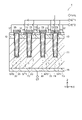
- 第1導電形の第1半導体層と、
前記第1半導体層上に設けられた第2導電形の第2半導体層と、
前記第2半導体層上に選択的に設けられた前記第1導電形の第3半導体層と、
前記第2半導体層上に選択的に設けられ、前記第3半導体層に並ぶ前記第2導電形の第4半導体層であって、前記第2半導体層の上面に平行な平面内において、前記第4半導体層の面積は、前記第3半導体層の面積よりも広い、第4半導体層と、
第2導電形の第5半導体層であって、前記第1半導体層は、前記第2半導体層と前記第5半導体層との間に位置する、第5半導体層と、
前記第3半導体層の上面から前記第1半導体層中に至る深さのトレンチの内部に設けられた制御電極であって、前記第1半導体層、前記第2半導体層および前記第3半導体層から第1絶縁膜により電気的に絶縁され、前記第2半導体層は、前記第1絶縁膜を介して前記制御電極に向き合い、前記第3半導体層は、前記第1絶縁膜に接した、制御電極と、
前記第3半導体層に電気的に接続された第1電極と、
前記第4半導体層に電気的に接続された第2電極と、
前記第5半導体層に電気的に接続された第3電極と、
前記制御電極に電気的接続された制御端子と、
を備えた半導体装置。 - 請求項1に記載の半導体装置の制御方法であって、
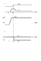
前記第2電極を介して前記第4半導体層に接続される電位を、前記第1電極を介して前記第3半導体層に接続される電位よりも低くする半導体装置の制御方法。 - 請求項1に記載の半導体装置の制御方法であって、
前記第1電極と前記第3電極との間の電圧が所定の値を超えた時、前記第2電極を介して前記第4半導体層に接続される電位を、前記第1電極を介して前記第3半導体層に接続される電位よりも低くする半導体装置の制御方法。 - 前記制御端子と前記第1電極との間に、前記制御電極のしきい値電圧よりも高い電圧を印加している間に、前記第4半導体層に接続される電位を、前記第1電極を介して前記第3半導体層に接続される電位よりも低くする請求項3記載の半導体装置の制御方法。
- 前記第2電極を介して前記第4半導体層に接続される電位を、前記第1電極を介して前記第3半導体層に接続される電位よりも低くする前に、前記第3半導体層と同じ電位を前記第2電極を介して前記第4半導体層に供給する請求項3または4に記載の半導体装置の制御方法。
Priority Applications (3)
| Application Number | Priority Date | Filing Date | Title |
|---|---|---|---|
| JP2020157529A JP7320910B2 (ja) | 2020-09-18 | 2020-09-18 | 半導体装置およびその制御方法 |
| US17/170,468 US11538929B2 (en) | 2020-09-18 | 2021-02-08 | Semiconductor device and method for controlling same |
| CN202110207897.5A CN114203811B (zh) | 2020-09-18 | 2021-02-24 | 半导体装置以及其控制方法 |
Applications Claiming Priority (1)
| Application Number | Priority Date | Filing Date | Title |
|---|---|---|---|
| JP2020157529A JP7320910B2 (ja) | 2020-09-18 | 2020-09-18 | 半導体装置およびその制御方法 |
Publications (2)
| Publication Number | Publication Date |
|---|---|
| JP2022051189A true JP2022051189A (ja) | 2022-03-31 |
| JP7320910B2 JP7320910B2 (ja) | 2023-08-04 |
Family
ID=80645764
Family Applications (1)
| Application Number | Title | Priority Date | Filing Date |
|---|---|---|---|
| JP2020157529A Active JP7320910B2 (ja) | 2020-09-18 | 2020-09-18 | 半導体装置およびその制御方法 |
Country Status (3)
| Country | Link |
|---|---|
| US (1) | US11538929B2 (ja) |
| JP (1) | JP7320910B2 (ja) |
| CN (1) | CN114203811B (ja) |
Citations (7)
| Publication number | Priority date | Publication date | Assignee | Title |
|---|---|---|---|---|
| JPH11345969A (ja) * | 1998-06-01 | 1999-12-14 | Toshiba Corp | 電力用半導体装置 |
| JP2008112936A (ja) * | 2006-10-31 | 2008-05-15 | Sanyo Electric Co Ltd | 絶縁ゲート型半導体装置 |
| JP2008227251A (ja) * | 2007-03-14 | 2008-09-25 | Mitsubishi Electric Corp | 絶縁ゲート型トランジスタ |
| US20120086045A1 (en) * | 2010-10-12 | 2012-04-12 | Io Semiconductor, Inc. | Vertical Semiconductor Device with Thinned Substrate |
| JP2012114321A (ja) * | 2010-11-26 | 2012-06-14 | Mitsubishi Electric Corp | 半導体装置 |
| JP2016167539A (ja) * | 2015-03-10 | 2016-09-15 | 株式会社東芝 | 半導体装置 |
| JP2017054935A (ja) * | 2015-09-09 | 2017-03-16 | 株式会社東芝 | 半導体装置 |
Family Cites Families (15)
| Publication number | Priority date | Publication date | Assignee | Title |
|---|---|---|---|---|
| JP2526960B2 (ja) | 1988-01-11 | 1996-08-21 | 日本電装株式会社 | 導電変調型mosfet |
| JP3182862B2 (ja) | 1991-05-31 | 2001-07-03 | 富士電機株式会社 | 半導体装置 |
| DE4216810C2 (de) | 1991-05-31 | 1999-09-16 | Fuji Electric Co Ltd | Steuerschaltung für einen Leitfähigkeitsänderungs-MISFET |
| JP3410286B2 (ja) * | 1996-04-01 | 2003-05-26 | 三菱電機株式会社 | 絶縁ゲート型半導体装置 |
| JP2003023157A (ja) * | 2001-07-09 | 2003-01-24 | Hitachi Ltd | 絶縁ゲートバイポーラトランジスタ |
| JP4114390B2 (ja) | 2002-04-23 | 2008-07-09 | 株式会社デンソー | 半導体装置及びその製造方法 |
| JP2012204436A (ja) * | 2011-03-24 | 2012-10-22 | Toshiba Corp | 電力用半導体装置 |
| JP6064371B2 (ja) * | 2012-05-30 | 2017-01-25 | 株式会社デンソー | 半導体装置 |
| JP6135636B2 (ja) * | 2014-10-17 | 2017-05-31 | トヨタ自動車株式会社 | 半導体装置 |
| JP7119378B2 (ja) * | 2017-03-15 | 2022-08-17 | 富士電機株式会社 | 半導体装置 |
| JP2019195007A (ja) | 2018-05-01 | 2019-11-07 | 良孝 菅原 | 半導体装置およびその製造方法 |
| JP2019220501A (ja) | 2018-06-15 | 2019-12-26 | 株式会社村田製作所 | 半導体装置 |
| JP7091204B2 (ja) * | 2018-09-19 | 2022-06-27 | 株式会社東芝 | 半導体装置 |
| JP6995722B2 (ja) * | 2018-09-19 | 2022-01-17 | 株式会社東芝 | 半導体装置 |
| US11276686B2 (en) * | 2019-05-15 | 2022-03-15 | Fuji Electric Co., Ltd. | Semiconductor device |
-
2020
- 2020-09-18 JP JP2020157529A patent/JP7320910B2/ja active Active
-
2021
- 2021-02-08 US US17/170,468 patent/US11538929B2/en active Active
- 2021-02-24 CN CN202110207897.5A patent/CN114203811B/zh active Active
Patent Citations (7)
| Publication number | Priority date | Publication date | Assignee | Title |
|---|---|---|---|---|
| JPH11345969A (ja) * | 1998-06-01 | 1999-12-14 | Toshiba Corp | 電力用半導体装置 |
| JP2008112936A (ja) * | 2006-10-31 | 2008-05-15 | Sanyo Electric Co Ltd | 絶縁ゲート型半導体装置 |
| JP2008227251A (ja) * | 2007-03-14 | 2008-09-25 | Mitsubishi Electric Corp | 絶縁ゲート型トランジスタ |
| US20120086045A1 (en) * | 2010-10-12 | 2012-04-12 | Io Semiconductor, Inc. | Vertical Semiconductor Device with Thinned Substrate |
| JP2012114321A (ja) * | 2010-11-26 | 2012-06-14 | Mitsubishi Electric Corp | 半導体装置 |
| JP2016167539A (ja) * | 2015-03-10 | 2016-09-15 | 株式会社東芝 | 半導体装置 |
| JP2017054935A (ja) * | 2015-09-09 | 2017-03-16 | 株式会社東芝 | 半導体装置 |
Also Published As
| Publication number | Publication date |
|---|---|
| US11538929B2 (en) | 2022-12-27 |
| CN114203811B (zh) | 2025-02-07 |
| JP7320910B2 (ja) | 2023-08-04 |
| US20220093776A1 (en) | 2022-03-24 |
| CN114203811A (zh) | 2022-03-18 |
Similar Documents
| Publication | Publication Date | Title |
|---|---|---|
| CN101499473B (zh) | 具有绝缘栅半导体元件的半导体器件和绝缘栅双极晶体管 | |
| US7476942B2 (en) | SOI lateral semiconductor device and method of manufacturing the same | |
| US10192978B2 (en) | Semiconductor apparatus | |
| JP6056202B2 (ja) | 半導体装置、半導体装置の制御方法および半導体装置の評価方法 | |
| JP2021048338A (ja) | 半導体装置及び半導体回路 | |
| JP7407757B2 (ja) | 半導体装置 | |
| US10840364B2 (en) | Semiconductor device | |
| CN115485857B (zh) | 半导体装置 | |
| JP2004296831A (ja) | 半導体装置 | |
| US20250294826A1 (en) | Igbt including field stop layer formed between collector layer and drift layer | |
| JP6302767B2 (ja) | 半導体装置及びそれを用いた電力変換装置 | |
| JP2022049611A (ja) | 半導体装置及び半導体回路 | |
| JP2021150544A (ja) | 半導体装置及び半導体回路 | |
| CN111326510B (zh) | 半导体装置 | |
| US12362744B2 (en) | Semiconductor device | |
| US10186571B2 (en) | Power semiconductor device and method therefor | |
| JP2021068845A (ja) | 半導体装置 | |
| JP7320910B2 (ja) | 半導体装置およびその制御方法 | |
| JP2022038486A (ja) | 試験装置、試験方法および製造方法 | |
| JP2021150528A (ja) | 半導体装置およびその制御方法 | |
| JP6038737B2 (ja) | 半導体装置及びそれを用いた電力変換装置 | |
| KR20190069183A (ko) | 절연 게이트 바이폴라 트랜지스터 및 그 제조 방법 | |
| JP2009021374A (ja) | 半導体装置 | |
| JP5588672B2 (ja) | 半導体装置の試験方法 | |
| JP2023138192A (ja) | 半導体装置及び半導体回路 |
Legal Events
| Date | Code | Title | Description |
|---|---|---|---|
| A621 | Written request for application examination |
Free format text: JAPANESE INTERMEDIATE CODE: A621 Effective date: 20220623 |
|
| A977 | Report on retrieval |
Free format text: JAPANESE INTERMEDIATE CODE: A971007 Effective date: 20230616 |
|
| TRDD | Decision of grant or rejection written | ||
| A01 | Written decision to grant a patent or to grant a registration (utility model) |
Free format text: JAPANESE INTERMEDIATE CODE: A01 Effective date: 20230623 |
|
| RD01 | Notification of change of attorney |
Free format text: JAPANESE INTERMEDIATE CODE: A7421 Effective date: 20230623 |
|
| A61 | First payment of annual fees (during grant procedure) |
Free format text: JAPANESE INTERMEDIATE CODE: A61 Effective date: 20230721 |
|
| R150 | Certificate of patent or registration of utility model |
Ref document number: 7320910 Country of ref document: JP Free format text: JAPANESE INTERMEDIATE CODE: R150 |