JP2023124231A - Acoustic wave devices, filters and multiplexers - Google Patents
Acoustic wave devices, filters and multiplexers Download PDFInfo
- Publication number
- JP2023124231A JP2023124231A JP2022027876A JP2022027876A JP2023124231A JP 2023124231 A JP2023124231 A JP 2023124231A JP 2022027876 A JP2022027876 A JP 2022027876A JP 2022027876 A JP2022027876 A JP 2022027876A JP 2023124231 A JP2023124231 A JP 2023124231A
- Authority
- JP
- Japan
- Prior art keywords
- piezoelectric layer
- thickness
- piezoelectric
- substrate
- acoustic wave
- Prior art date
- Legal status (The legal status is an assumption and is not a legal conclusion. Google has not performed a legal analysis and makes no representation as to the accuracy of the status listed.)
- Granted
Links
Images





Classifications
-
- H—ELECTRICITY
- H03—ELECTRONIC CIRCUITRY
- H03H—IMPEDANCE NETWORKS, e.g. RESONANT CIRCUITS; RESONATORS
- H03H9/00—Networks comprising electromechanical or electro-acoustic elements; Electromechanical resonators
- H03H9/02—Details
- H03H9/02007—Details of bulk acoustic wave devices
- H03H9/02015—Characteristics of piezoelectric layers, e.g. cutting angles
-
- H—ELECTRICITY
- H03—ELECTRONIC CIRCUITRY
- H03H—IMPEDANCE NETWORKS, e.g. RESONANT CIRCUITS; RESONATORS
- H03H9/00—Networks comprising electromechanical or electro-acoustic elements; Electromechanical resonators
- H03H9/15—Constructional features of resonators consisting of piezoelectric or electrostrictive material
- H03H9/17—Constructional features of resonators consisting of piezoelectric or electrostrictive material having a single resonator
- H03H9/171—Constructional features of resonators consisting of piezoelectric or electrostrictive material having a single resonator implemented with thin-film techniques, i.e. of the film bulk acoustic resonator [FBAR] type
- H03H9/172—Means for mounting on a substrate, i.e. means constituting the material interface confining the waves to a volume
- H03H9/173—Air-gaps
-
- H—ELECTRICITY
- H03—ELECTRONIC CIRCUITRY
- H03H—IMPEDANCE NETWORKS, e.g. RESONANT CIRCUITS; RESONATORS
- H03H9/00—Networks comprising electromechanical or electro-acoustic elements; Electromechanical resonators
- H03H9/02—Details
- H03H9/02007—Details of bulk acoustic wave devices
- H03H9/02157—Dimensional parameters, e.g. ratio between two dimension parameters, length, width or thickness
-
- H—ELECTRICITY
- H03—ELECTRONIC CIRCUITRY
- H03H—IMPEDANCE NETWORKS, e.g. RESONANT CIRCUITS; RESONATORS
- H03H9/00—Networks comprising electromechanical or electro-acoustic elements; Electromechanical resonators
- H03H9/02—Details
- H03H9/125—Driving means, e.g. electrodes, coils
- H03H9/13—Driving means, e.g. electrodes, coils for networks consisting of piezoelectric or electrostrictive materials
- H03H9/133—Driving means, e.g. electrodes, coils for networks consisting of piezoelectric or electrostrictive materials for electromechanical delay lines or filters
-
- H—ELECTRICITY
- H03—ELECTRONIC CIRCUITRY
- H03H—IMPEDANCE NETWORKS, e.g. RESONANT CIRCUITS; RESONATORS
- H03H9/00—Networks comprising electromechanical or electro-acoustic elements; Electromechanical resonators
- H03H9/15—Constructional features of resonators consisting of piezoelectric or electrostrictive material
- H03H9/17—Constructional features of resonators consisting of piezoelectric or electrostrictive material having a single resonator
- H03H9/171—Constructional features of resonators consisting of piezoelectric or electrostrictive material having a single resonator implemented with thin-film techniques, i.e. of the film bulk acoustic resonator [FBAR] type
- H03H9/172—Means for mounting on a substrate, i.e. means constituting the material interface confining the waves to a volume
- H03H9/175—Acoustic mirrors
-
- H—ELECTRICITY
- H03—ELECTRONIC CIRCUITRY
- H03H—IMPEDANCE NETWORKS, e.g. RESONANT CIRCUITS; RESONATORS
- H03H9/00—Networks comprising electromechanical or electro-acoustic elements; Electromechanical resonators
- H03H9/46—Filters
- H03H9/54—Filters comprising resonators of piezoelectric or electrostrictive material
- H03H9/56—Monolithic crystal filters
- H03H9/566—Electric coupling means therefor
- H03H9/568—Electric coupling means therefor consisting of a ladder configuration
-
- H—ELECTRICITY
- H03—ELECTRONIC CIRCUITRY
- H03H—IMPEDANCE NETWORKS, e.g. RESONANT CIRCUITS; RESONATORS
- H03H9/00—Networks comprising electromechanical or electro-acoustic elements; Electromechanical resonators
- H03H9/70—Multiple-port networks for connecting several sources or loads, working on different frequencies or frequency bands, to a common load or source
- H03H9/703—Networks using bulk acoustic wave devices
- H03H9/706—Duplexers
-
- H—ELECTRICITY
- H03—ELECTRONIC CIRCUITRY
- H03H—IMPEDANCE NETWORKS, e.g. RESONANT CIRCUITS; RESONATORS
- H03H9/00—Networks comprising electromechanical or electro-acoustic elements; Electromechanical resonators
- H03H9/02—Details
- H03H9/02007—Details of bulk acoustic wave devices
- H03H9/02015—Characteristics of piezoelectric layers, e.g. cutting angles
- H03H9/02031—Characteristics of piezoelectric layers, e.g. cutting angles consisting of ceramic
Landscapes
- Physics & Mathematics (AREA)
- Acoustics & Sound (AREA)
- Chemical & Material Sciences (AREA)
- Crystallography & Structural Chemistry (AREA)
- Surface Acoustic Wave Elements And Circuit Networks Thereof (AREA)
- Piezo-Electric Or Mechanical Vibrators, Or Delay Or Filter Circuits (AREA)
Abstract
Description
本発明は、弾性波デバイス、フィルタおよびマルチプレクサに関し、例えば、共振器を有する弾性波デバイス、フィルタおよびマルチプレクサに関する。 The present invention relates to acoustic wave devices, filters and multiplexers, for example acoustic wave devices, filters and multiplexers having resonators.
携帯電話等の無線端末の高周波回路用のフィルタおよびデュプレクサとして、FBAR(Film Bulk Acoustic Resonator)およびSMR(Solid Mounted Resonator)等のBAW(Bulk Acoustic Wave)共振器が用いられている。BAW共振器は圧電薄膜共振器とよばれている。圧電薄膜共振器は、圧電層を挟み一対の電極を設ける構造を有し、圧電層の少なくとも一部を挟み一対の電極が対向する共振領域は弾性波が共振する領域である。圧電層として、自発分極が反対方向である2つの圧電層を積層することが知られている(例えば特許文献1~5)。積層する2つの圧電層を単結晶ニオブ酸リチウム基板と単結晶タンタル酸リチウム基板とすることが知られている(例えば特許文献5)。
BAW (Bulk Acoustic Wave) resonators such as FBAR (Film Bulk Acoustic Resonator) and SMR (Solid Mounted Resonator) are used as filters and duplexers for high-frequency circuits of wireless terminals such as mobile phones. A BAW resonator is called a piezoelectric thin film resonator. A piezoelectric thin film resonator has a structure in which a pair of electrodes are provided with a piezoelectric layer sandwiched therebetween. A resonance region where the pair of electrodes face each other with at least a portion of the piezoelectric layer sandwiched therebetween is a region in which elastic waves resonate. As a piezoelectric layer, it is known to laminate two piezoelectric layers having spontaneous polarizations in opposite directions (for example,
自発分極の方向が互いに逆方向の圧電層を積層することで、第2高調波の弾性波を励振させることができる。第2高調波の弾性波を主モードとして用いる場合、基本波は不要波となる。積層された圧電層の一方を回転Yカットニオブ酸リチウム基板とし、他方を回転Yカットタンタル酸リチウム基板とする場合、不要波である基本波の励振を抑制することが求められる。 By laminating piezoelectric layers having spontaneous polarization directions opposite to each other, the elastic wave of the second harmonic can be excited. When the elastic wave of the second harmonic is used as the main mode, the fundamental wave becomes an unwanted wave. When one of the laminated piezoelectric layers is a rotated Y-cut lithium niobate substrate and the other is a rotated Y-cut lithium tantalate substrate, it is required to suppress the excitation of the fundamental wave, which is an unnecessary wave.
本発明は、上記課題に鑑みなされたものであり、不要波を抑制することを目的とする。 The present invention has been made in view of the above problems, and an object of the present invention is to suppress unnecessary waves.
本発明は、回転Yカットタンタル酸リチウム基板であり、第1厚さを有する第1圧電層と、回転Yカットニオブ酸リチウム基板であり、前記第1圧電層に積層され、前記第1厚さより小さい第2厚さを有し、前記第1圧電層の自発分極の方向と略反対方向の自発分極の方向を有する第2圧電層と、前記第1圧電層の前記第2圧電層に対し反対の面に設けられた第1電極と、前記第2圧電層の前記第1圧電層に対し反対の面に設けられ、前記第1電極とで前記第1圧電層の少なくとも一部および前記第2圧電層の少なくとも一部を挟む第2電極と、を備える弾性波デバイスである。 The present invention is a rotated Y-cut lithium tantalate substrate, a first piezoelectric layer having a first thickness; and a rotated Y-cut lithium niobate substrate, laminated to the first piezoelectric layer, and having a thickness greater than the first thickness. a second piezoelectric layer having a smaller second thickness and having a direction of spontaneous polarization substantially opposite to the direction of spontaneous polarization of the first piezoelectric layer; and a direction of spontaneous polarization of the first piezoelectric layer opposite to the second piezoelectric layer. and a first electrode provided on the surface of the second piezoelectric layer opposite to the first piezoelectric layer. and a second electrode sandwiching at least a portion of the piezoelectric layer.
上記構成において、前記第1圧電層は、158°以上かつ168°以下回転Yカットタンタル酸リチウム基板であり、前記第2圧電層は、158°以上かつ168°以下回転Yカットニオブ酸リチウム基板であり、前記第2厚さは前記第1厚さの0.5倍以上である構成とすることができる。 In the above configuration, the first piezoelectric layer is a Y-cut lithium tantalate substrate rotated by 158° or more and 168° or less, and the second piezoelectric layer is a Y-cut lithium niobate substrate rotated by 158° or more and 168° or less. and the second thickness may be 0.5 times or more the first thickness.
上記構成において、前記第2厚さは前記第1厚さの0.56倍以上かつ0.92倍以下である構成とすることができる。 In the above configuration, the second thickness may be 0.56 times or more and 0.92 times or less the first thickness.
上記構成において、前記第2厚さは前記第1厚さの0.68倍以上かつ0.78倍以下である構成とすることができる。 In the above configuration, the second thickness may be 0.68 times or more and 0.78 times or less the first thickness.
上記構成において、前記第1圧電層における回転Yカットタンタル酸リチウム基板の結晶方位のX軸方向と、前記第1圧電層における回転Yカットニオブ酸リチウム基板の結晶方位のX軸方向と、のなす角度は5°以下である構成とすることができる。 In the above configuration, the X-axis direction of the crystal orientation of the rotated Y-cut lithium tantalate substrate in the first piezoelectric layer and the X-axis direction of the crystal orientation of the rotated Y-cut lithium niobate substrate in the first piezoelectric layer form. The angle may be configured to be 5° or less.
上記構成において、前記第1圧電層と前記第2圧電層とは直接接合されている構成とすることができる。 In the above structure, the first piezoelectric layer and the second piezoelectric layer may be directly bonded.
上記構成において、支持基板を備え、前記第1圧電層は前記支持基板と前記第2圧電層との間に設けられている構成とすることができる。 In the above configuration, a support substrate may be provided, and the first piezoelectric layer may be provided between the support substrate and the second piezoelectric layer.
上記構成において、支持基板を備え、前記第2圧電層は前記支持基板と前記第1圧電層との間に設けられている構成とすることができる。 In the above configuration, a support substrate may be provided, and the second piezoelectric layer may be provided between the support substrate and the first piezoelectric layer.
本発明は、上記弾性波デバイスを含むフィルタである。 The present invention is a filter including the above acoustic wave device.
本発明は、上記フィルタを含むマルチプレクサである。 The present invention is a multiplexer including the above filters.
本発明によれば、電気機械結合係数を調整可能とすることができる。 According to the present invention, the electromechanical coupling coefficient can be made adjustable.
以下、図面を参照し本発明の実施例について説明する。 Hereinafter, embodiments of the present invention will be described with reference to the drawings.
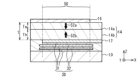
弾性波デバイスとして圧電薄膜共振器を例に説明する。図1(a)は、実施例1に係る圧電薄膜共振器の平面図、図1(b)は、図1(a)のA-A断面図である。圧電層14aおよび14bの積層方向をZ方向、下部電極12の引き出し方向をX方向、X方向およびZ方向に直交する方向をY方向とする。
A piezoelectric thin film resonator will be described as an example of an acoustic wave device. FIG. 1(a) is a plan view of a piezoelectric thin film resonator according to Example 1, and FIG. 1(b) is a cross-sectional view taken along the line AA of FIG. 1(a). The stacking direction of the
図1(a)および図1(b)に示すように、基板10上に圧電層14が設けられている。圧電層14は、積層された圧電層14aおよび14bを備える。圧電層14aおよび14bの厚さはそれぞれTaおよびTbである。圧電層14の厚さはTである。圧電層14aは回転Yカットニオブ酸リチウム(LiNbO3)基板であり、圧電層14bは回転Yカットタンタル酸リチウム(LiTaO3)基板である。圧電層14aの分極方向52aは下向きである。圧電層14bの分極方向52bは上向きであり、圧電層14aと14bとは例えば表面活性化法により直接接合されている。圧電層14aと14bとが表面活性化法により接合されている場合、圧電層14aと14bとの間にアモルファス層が形成される場合がある。この場合、アモルファス層の厚さは圧電層14aおよび14bの厚さに比べ十分小さいため、圧電層14aと14bとは直接接合されているとみなせる。
As shown in FIGS. 1(a) and 1(b), a
圧電層14の上下に上部電極16および下部電極12がそれぞれ設けられている。圧電層14aの少なくとも一部および圧電層14bの少なくとも一部を挟み下部電極12と上部電極16とが平面視において重なる領域は共振領域50である。基板10と下部電極12との間に空隙34が設けられている。下部電極12と空隙34との界面において弾性波が反射する。平面視において、空隙34は共振領域50に重なり、空隙34は共振領域50と同じ大きさまたは共振領域50より大きい。
An
基板10は、例えばシリコン基板、サファイア基板、アルミナ基板、スピネル基板、石英基板、水晶基板、ガラス基板、セラミック基板またはGaAs基板等である。下部電極12および上部電極16は、例えばルテニウム(Ru)、クロム(Cr)、アルミニウム(Al)、チタン(Ti)、銅(Cu)、モリブデン(Mo)、タングステン(W)、タンタル(Ta)、白金(Pt)、ロジウム(Rh)またはイリジウム(Ir)等の単層膜またはこれらの膜を積層した積層膜である。
The
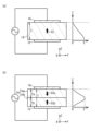
図2(a)および図2(b)は、比較例1および実施例1における圧電薄膜共振器の動作を説明する図である。図2(a)および図2(b)では、下部電極12、圧電層14および上部電極16を示す。右側の図は、Z方向の位置に対する弾性波の変位を示す図である。なお、図2(b)において、説明を簡単にするため厚さTaとTbとを同じとして図示している。
2A and 2B are diagrams for explaining the operation of the piezoelectric thin film resonators in Comparative Example 1 and Example 1. FIG. 2(a) and 2(b), the
図2(a)に示すように、比較例1では、圧電層14は分極方向52が1方向の1つの圧電層である。この場合、右図のように、基本波では圧電層14の上面の変位が0のとき、圧電層14の下面の変位がEとなる。これにより、基本波では、下部電極12と上部電極16との電位が異なり、下部電極12と上部電極16との間に所定の周波数の交流信号を加えると圧電層14に基本波が励振する。一方、第2高調波では下部電極12と上部電極16との電位がほぼ同じとなる。よって、圧電層14に第2高調波はほとんど励振されない。圧電層14の厚さTは基本波の波長のほぼ1/2となる。共振周波数の高い圧電薄膜共振器を作製するためには、圧電層14の厚さTを薄くすることになる。しかし、圧電層14と支持基板との間に空隙34が存在するため、圧電層14を薄くすると、圧電層14が破壊されやすくなる。また、圧電層14の厚さTの製造ばらつきにより、共振周波数等の特性がばらつきやすくなる。
As shown in FIG. 2A, in Comparative Example 1, the
図2(b)に示すように、実施例1では、圧電層14aの分極方向52aは下向き、圧電層14bの分極方向52bは上向きである。右図のように、第2高調波では圧電層14の上面の変位が0のとき、圧電層14の下面の変位が0である。圧電層14のZ方向のほぼ中央付近の変位はEである。圧電層14aの分極方向52aと圧電層14bの分極方向52bとは逆方向のため、第2高調波では下部電極12と上部電極16との電位が異なる、下部電極12と上部電極16との間に所定の周波数の交流信号を加えると第2高調波が励振する。一方、基本波では下部電極12と上部電極16との電位がほぼ同じとなる。よって、圧電層14に基本波はほとんど励振されない。厚さTはほぼ第2高調波の波長となる。このため、同じ共振周波数を有する圧電薄膜共振器を作製する場合に、実施例1では、比較例1に対し、圧電層14の厚さTを約2倍にできる。これにより、圧電層14の破損を抑制できる。また、共振周波数等の特性のばらつきを抑制できる。
As shown in FIG. 2B, in Example 1, the
圧電層14aおよび14bに回転カット角が163°のタンタル酸リチウム基板また回転カット角が163°のニオブ酸リチウム基板を用いると、圧電層14に厚みすべり振動が励起される。厚みすべりの振動方向はY方向となる。また、圧電層14には厚み縦振動はほとんど励振されない。このことから、厚みすべり振動を主モードとする場合、回転カット角が163°とすることが好ましい。
When a lithium tantalate substrate with a rotation cut angle of 163° or a lithium niobate substrate with a rotation cut angle of 163° is used for the
圧電層14aと14bを同じ材料とする場合、圧電特性は材料により決まってしまう。そこで、圧電層14aをタンタル酸リチウム基板とし、圧電層14bをニオブ酸リチウム基板とすることで、電気機械結合係数k2等の圧電特性を、圧電層14aと14bをタンタル酸リチウム基板とした場合の圧電特性と、圧電層14aと14bをニオブ酸リチウム基板とした場合の圧電特性と、の間にすることができる。
If the
図3は、実施例1における圧電層の結晶方位を示す図である。なお、X軸方向、Y軸方向およびZ軸方向は結晶方位の軸方向であり、X方向、Y方向およびZ方向は、図1(a)および図1(b)に示した方向である。圧電層14aとして、163°回転Yカットニオブ酸リチウム基板を用い、圧電層14bとして、163°回転Yカットタンタル酸リチウム基板を用いている。
FIG. 3 is a diagram showing the crystal orientation of the piezoelectric layer in Example 1. FIG. The X-axis direction, Y-axis direction and Z-axis direction are crystal orientation axial directions, and the X-, Y- and Z-directions are the directions shown in FIGS. 1(a) and 1(b). A 163° rotated Y-cut lithium niobate substrate is used as the
図3に示すように、圧電層14aの結晶方位の+X軸方向と圧電層14bの結晶方位の+X軸方向とはほぼ同じ方向であり、X方向である。圧電層14aでは、+Y軸方向および+Z軸方向を破線矢印のように、それぞれ-Z方向および+Y方向とする。X軸を中心に、Y軸およびZ軸を+Z軸方向から+Y軸方向の方にθ=163°回転させる。タンタル酸リチウム基板およびニオブ酸リチウム基板は、三方晶系イルメナイトに類似の結晶構造を有し、+Z軸方向が結晶方位のc軸方向に対応する。+Z軸方向が自発分極の方向となる。このとき、圧電層14aの上面および下面はそれぞれ-面および+面と称し、分極方向52aを下向きに図示する。
As shown in FIG. 3, the +X-axis direction of the crystal orientation of the
圧電層14bでは、+Y軸方向および+Z軸方向を破線矢印のように、それぞれ+Z方向および-Y方向とする。X軸を中心に、Y軸およびZ軸を+Z軸方向から+Y軸方向の方にθ=163°回転させる。このときの+Z軸方向が結晶方位のc軸方向に対応する。+Z軸方向が自発分極の方向となる。このとき、圧電層14bの上面および下面はそれぞれ+面および-面と称し、分極方向52bを上向きに図示する。圧電層14aおよび14bの自発分極の方向は、X線回折法を用い、Z軸方向を同定することで、確認できる。
In the
自発分極は電界が加わらない状態で分極している状態である。タンタル酸リチウムは、LiおよびTaが陽イオンとなり、Oが陰イオンとなる。Li、TaおよびOの原子が電荷を打ち消すように位置していれば、自発分極は生じない。これらの原子が電荷を打ち消す位置よりずれているため、自発分極が生じる。ニオブ酸リチウムにおいても同様に自発分極が生じる。 Spontaneous polarization is a state of polarization in the absence of an electric field. In lithium tantalate, Li and Ta are cations and O is an anion. Spontaneous polarization does not occur if the Li, Ta and O atoms are positioned to cancel their charges. Spontaneous polarization occurs because these atoms are out of position to cancel charge. Spontaneous polarization also occurs in lithium niobate.
圧電層14aの+X軸方向と圧電層14bの+X軸方向とを略同じ方向とすることで、圧電層14aの自発分極の方向(+Z軸方向)と圧電層14bの自発分極の方向(+Z軸方向)は、略反対方向となる。例えば、圧電層14aの+X軸方向と圧電層14bのX軸方向とが異なると、圧電層14aの自発分極の方向(+Z軸方向)と圧電層14bの自発分極の方向(+Z軸方向)は、反対方向とはならない。圧電層14aの自発分極の方向(+Z軸方向)と圧電層14bの自発分極の方向(+Z軸の方向)とが略反対方向とは、圧電層14aの+X軸方向と圧電層14bの+X軸方向とのなす角度が5°以下の範囲内である程度を許容する。
By making the +X-axis direction of the
[シミュレーション]
圧電薄膜共振器の周波数特性を有限要素法を用いシミュレーションした。シミュレーション条件は以下である。
圧電層14の厚さT:300nm
下部電極12:厚さが30nmのアルミニウム膜
上部電極16:厚さが30nmのアルミニウム膜
圧電層14bの厚さTbに対する圧電層14aの厚さTaをTa/Tbとした。Ta/Tb=1のとき、圧電層14aおよび14bの厚さTaおよびTbはいずれも150nmである。
[simulation]
The frequency characteristics of a piezoelectric thin film resonator were simulated using the finite element method. The simulation conditions are as follows.
Thickness T of piezoelectric layer 14: 300 nm
Lower electrode 12: Aluminum film with a thickness of 30 nm Upper electrode 16: Aluminum film with a thickness of 30 nm The thickness Ta of the
比較例2として、圧電層14aおよび14bをともに163°回転Yカットニオブ酸リチウム基板を用いた場合における周波数特性をシミュレーションした。圧電層14aと圧電層14bとは、分極方向が互いに反対方向となるように接合されている。図4は、比較例2における周波数に対する|Y|を示す図である。|Y|はアドミッタンスの絶対値である。図4に示すように、Ta/Tb=1のとき、第2高調波による弾性波の応答として、共振周波数fr2および反共振周波数fa2が観察される。基本波の応答は観測されない。Ta/Tb=0.9048のとき、第2高調波による弾性波の応答として、共振周波数fr2および反共振周波数fa2が観察され、かつ基本波の弾性波の応答として、共振周波数fr1および反共振周波数fa1が観察される。
As Comparative Example 2, the frequency characteristics were simulated in the case of using Y-cut lithium niobate substrates rotated by 163° for both the
比較例2のように、圧電層14aと14bとを同じ材料とした場合、Ta/Tb=1とすることで、不要波である基本波はほとんど励振されない。一方、Ta/Tbを1から異ならせると、不要波である基本波が励振される。
When the
実施例1として、圧電層14aに163°回転Yカットニオブ酸リチウム基板を用い、圧電層14bに163°回転Yカットタンタル酸リチウム基板を用いた場合における周波数特性をシミュレーションした。圧電層14aと圧電層14bとは、分極方向が互いに反対方向となるように接合されている。図5は、実施例1における周波数に対する|Y|を示す図である。|Y|はアドミッタンスの絶対値である。図5に示すように、Ta/Tb=1のとき、第2高調波による弾性波の応答として、共振周波数fr2および反共振周波数fa2が観察されかつ基本波の弾性波の応答として、共振周波数fr1および反共振周波数fa1が観察される。Ta/Tb=0.7178のとき、第2高調波による弾性波の応答として、共振周波数fr2および反共振周波数fa2が観察され、基本波の応答は観測されない。
As Example 1, a 163° rotated Y-cut lithium niobate substrate was used for the
このように、圧電層14aに回転Yカットニオブ酸リチウム基板を用い、圧電層14bに回転Yカットタンタル酸リチウム基板を用いた場合、厚さTaを厚さTbより小さくすることで基本波を抑制することができる。そこで、Ta/Tbを変え、基本波の電気機械結合係数k2をシミュレーションした。
Thus, when the rotated Y-cut lithium niobate substrate is used for the
図6(a)は、Ta/Tbに対する基本波のk2を示す図、図6(b)は、Ta/Tbに対する基本波のΔk2を示す図である。図6(a)において、黒丸はシミュレーションした点を示し、曲線は黒丸をつなぐ線である。図6(b)において、Δk2は、Ta/Tbに対するk2の変化率であり、図6(a)の隣接する黒丸間の傾きに相当する。 FIG. 6(a) is a diagram showing k2 of the fundamental wave with respect to Ta/Tb, and FIG. 6(b) is a diagram showing Δk2 of the fundamental wave with respect to Ta/Tb. In FIG. 6(a), black circles indicate simulated points, and curves are lines connecting the black circles. In FIG. 6(b), Δk2 is the rate of change of k2 with respect to Ta/Tb and corresponds to the slope between adjacent black circles in FIG. 6(a).
図6(a)および図6(b)に示すように、基本波の電気機械結合係数k2はTa/Tbが0.70~0.75において0.06程度となる。Ta/Tbが0.7以下ではTa/Tbが小さくなるとk2が大きくなり、Ta/Tbが0.75以上ではTa/Tbが大きくなるとk2が大きくなる。 As shown in FIGS. 6A and 6B, the electromechanical coupling coefficient k2 of the fundamental wave is about 0.06 when Ta/Tb is 0.70 to 0.75. When Ta/Tb is 0.7 or less, k2 increases as Ta/Tb decreases, and when Ta/Tb is 0.75 or more, k2 increases as Ta/Tb increases.
θを158°、163°および168°に設定し、Ta/Tbを変え、基本波のk2をシミュレーションした。図7は、Ta/Tbに対する基本波のk2を示す図である。図7に示すように、θが158°、163°および168°のいずれにおいても基本波のk2は0.70~0.75において最小となる。範囲R1~R3は、θがそれぞれ158°、163°および168°のときに、基本波のk2がTa/Tb=1のときのk2(Ta/Tb=1)より小さくなる範囲である。Ta/Tbが範囲R1~R3内であれば、基本波のk2は、Ta/Tb=1のときのk2(Ta/Tb=1)以下となる。 θ was set to 158°, 163° and 168°, Ta/Tb was changed, and k2 of the fundamental wave was simulated. FIG. 7 is a diagram showing k2 of the fundamental wave with respect to Ta/Tb. As shown in FIG. 7, k2 of the fundamental wave is minimum at 0.70 to 0.75 at θ of 158°, 163° and 168°. Ranges R1 to R3 are ranges in which k 2 of the fundamental wave is smaller than k 2 (Ta/Tb=1) when Ta/Tb=1 when θ is 158°, 163° and 168°, respectively. . If Ta/Tb is within the range R1 to R3, k 2 of the fundamental wave is equal to or less than k 2 (Ta/Tb=1) when Ta/Tb=1.
図8は、Ta/Tbに対するk2およびk2/k2(Ta/Tb=1)を示す図である。θが158°、163°および168°において、k2/k2(Ta/Tb=1)が1.0、0.8、0.6、0.5、0.4および0.2となるTa/Tbと、k2が0.1%となるTa/Tbを示している。 FIG. 8 is a diagram showing k 2 and k 2 /k 2 (Ta/Tb=1) versus Ta/Tb. When θ is 158°, 163° and 168°, k 2 /k 2 (Ta/Tb=1) is 1.0, 0.8, 0.6, 0.5, 0.4 and 0.2 Ta/Tb and Ta/Tb at which k2 is 0.1% are shown.
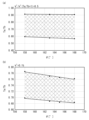
図9(a)および図9(b)は、θに対するTa/Tbを示す図である。図9(a)は、k2/k2(Ta/Tb=1)が0.5より小さくなるTa/Tbの範囲を示し、図9(b)は、基本波のk2が0.1%以下となる範囲を示している。図9(a)および図9(b)において、黒丸はシミュレーション点を示し、直線は黒丸の近似直線、ハッチは直線間の範囲を示している。 FIGS. 9(a) and 9(b) are diagrams showing Ta/Tb with respect to θ. FIG. 9(a) shows the range of Ta/Tb where k 2 /k 2 (Ta/Tb=1) is smaller than 0.5, and FIG. 9(b) shows that the fundamental wave k 2 is 0.1 % or less. In FIGS. 9A and 9B, black circles indicate simulation points, straight lines are approximate straight lines of the black circles, and hatching indicates the range between the straight lines.
図9(a)および図9(b)に示すように、k2/k2(Ta/Tb=1)が0.5より小さくなるTa/Tbの範囲、および基本波のk2が0.1%以下となるTa/Tbの範囲は、θにあまり依存しない。 As shown in FIGS. 9A and 9B, the Ta/Tb range where k 2 /k 2 (Ta/Tb=1) is less than 0.5 and the fundamental wave k 2 is 0.5. The range of Ta/Tb, which is 1% or less, does not greatly depend on θ.
実施例1によれば、図1(a)および図1(b)のように、圧電層14b(第1圧電層)と圧電層14a(第2圧電層)は積層されている。圧電層14bは、回転Yカットタンタル酸リチウム基板であり、厚さTb(第1厚さ)を有する。圧電層14aは、回転Yカットニオブ酸リチウム基板であり、厚さTa(第2厚さ)を有し、圧電層14bの自発分極の方向と略反対方向の自発分極の方向を有する。下部電極12(第1電極)は、圧電層14bの圧電層14aに対し反対の面に設けられている。上部電極16(第2電極)は、圧電層14aの圧電層14bに対し反対の面に設けられ、下部電極12とで圧電層14bの少なくとも一部および圧電層14aの少なくとも一部を挟む。このような構造において、厚さTaを厚さTbより小さくする。これにより、基本波のk2を小さくすることができ、不要波を抑制できる。なお、圧電層14aと14bとの自発分極の方向が略反対方向とは、基本波を抑制できる程度に反対方向であればよい。圧電層14aと14bとの自発分極の方向のなす角度は、175°以上かつ185°以下であることが好ましく、177°以上かつ183°以下であることがより好ましく、178°以上かつ182°以下であることがさらに好ましい。
According to Example 1, as shown in FIGS. 1A and 1B, the
図8から図9(b)より、基本波の大きさはθにあまり依存しない。このことから、圧電層14bは、158°以上かつ168°以下回転Yカットタンタル酸リチウム基板であり、圧電層14aは、158°以上かつ168°以下回転Yカットニオブ酸リチウム基板であれば、図8から図9(b)と同様の結果が得られると考えられる。図8より、厚さTaは厚さTbの0.5倍以上であれば、k2/k2(Ta/Tb=1)を1より小さくできる。厚みすべり振動の弾性波を励振させ、厚み縦振動の弾性波を励振させないため、圧電層14bおよび14aのθは、160°以上かつ166°以下が好ましく、161°以上かつ165°以下がより好ましい。
8 to 9B, the magnitude of the fundamental wave does not depend much on θ. Therefore, if the
図8より、Ta/Tbが0.52以上かつ0.97以下のとき、k2/k2(Ta/Tb=1)を0.8以下にできる。Ta/Tbが0.55以上かつ0.94以下のとき、k2/k2(Ta/Tb=1)を0.6以下にできる。Ta/Tbが0.56以上かつ0.92以下のとき、k2/k2(Ta/Tb=1)を0.5以下にできる。Ta/Tbが0.58以上かつ0.90以下のとき、k2/k2(Ta/Tb=1)を0.4以下にできる。Ta/Tbが0.62以上かつ0.85以下のとき、k2/k2(Ta/Tb=1)を0.2以下にできる。Ta/Tbが0.68以上かつ0.78以下のとき、k2を0.1%以下にできる。 From FIG. 8, when Ta/Tb is 0.52 or more and 0.97 or less, k 2 /k 2 (Ta/Tb=1) can be made 0.8 or less. When Ta/Tb is 0.55 or more and 0.94 or less, k 2 /k 2 (Ta/Tb=1) can be 0.6 or less. When Ta/Tb is 0.56 or more and 0.92 or less, k 2 /k 2 (Ta/Tb=1) can be made 0.5 or less. When Ta/Tb is 0.58 or more and 0.90 or less, k 2 /k 2 (Ta/Tb=1) can be made 0.4 or less. When Ta/Tb is 0.62 or more and 0.85 or less, k 2 /k 2 (Ta/Tb=1) can be 0.2 or less. When Ta/Tb is 0.68 or more and 0.78 or less, k2 can be 0.1% or less.
圧電層14aの自発分極の方向と圧電層14bの自発分極の方向とを略反対方向とするため、圧電層14aにおけるタンタル酸リチウム基板の結晶方位のX軸方向と、圧電層14bにおけるニオブ酸リチウム基板の結晶方位のX軸方向と、のなす角度は5°以下であることが好ましく、2°以下であることがより好ましい。
Since the direction of spontaneous polarization of the
圧電層14aと14bとは直接接合され、圧電層14aと14bとの界面は平坦面(例えば算術表面粗さRaは10nm以下)である。これにより、圧電層14に第2高調波が励振できる。
The
[実施例1の変形例1]
図10(a)から図10(c)は、実施例1の変形例1から3に係る圧電薄膜共振器の断面図である。図10(a)に示すように、実施例1の変形例1では、圧電層14aの分極方向52aが上方向であり、圧電層14bの分極方向52bが下方向である。その他の構成は実施例1と同じであり説明を省略する。
[
10A to 10C are cross-sectional views of piezoelectric thin film resonators according to
[実施例1の変形例2]
図10(b)に示すように、実施例1の変形例2では、圧電層14aの上面と圧電層14bの下面が接合されており、圧電層14aの下面に下部電極12が設けられ、圧電層14bの上面に上部電極16が設けられている。圧電層14aの分極方向52aは上方向であり、圧電層14bの分極方向52bは下方向である。その他の構成は実施例1と同じであり説明を省略する。
[
As shown in FIG. 10B, in Modified Example 2 of Example 1, the upper surface of the
[実施例1の変形例3]
図10(c)に示すように、実施例1の変形例3では、圧電層14aの分極方向52aは下方向であり、圧電層14bの分極方向52bは上方向である。その他の構成は実施例1の変形例2と同じであり説明を省略する。
[
As shown in FIG. 10C, in
実施例1およびその変形例1のように、圧電層14bは基板10(支持基板)と圧電層14aとの間に設けられていてもよい。実施例1の変形例2および3のように、圧電層14aは基板10と圧電層14bとの間に設けられていてもよい。基本波を抑制するTa/Tbは、基本波が励振したときに、自発分極によって発生する電荷量で決まる。このため、上記シミュレーションによって得られたTa/Tbの好ましい範囲は、実施例1の変形例1から3にも適用できる。また、好ましいTa/Tbの範囲は、圧電薄膜共振器の共振周波数等の周波数、下部電極12および上部電極16の材料、並びに圧電層14a、14b、下部電極12および上部電極16に依存せず適用できる。
The
[実施例1の変形例4]
図11は、実施例1の変形例4に係る圧電薄膜共振器の断面図である。図11に示すように、実施例1の変形例4では、空隙34の代わりに、基板10と下部電極12との間に音響反射膜30が設けられている。音響反射膜30は、音響インピーダンスの低い膜31と音響インピーダンスの高い膜32とが交互に設けられている。膜31および32の膜厚は例えばそれぞれほぼλ/4(λは弾性波の波長)である。これにより、音響反射膜30は弾性波を反射する。膜31と膜32の積層数は任意に設定できる。音響反射膜30は共振領域50に重なり、音響反射膜30は共振領域50と同じ大きさまたは共振領域50より大きい。音響反射膜30の膜31は、例えば酸化シリコン、窒化シリコン等である。膜32は、例えばタングステン、タンタル、モリブデン、ルテニウム等である。
[
11 is a cross-sectional view of a piezoelectric thin film resonator according to
実施例1およびその変形例1から3のように、圧電薄膜共振器は、空隙34が弾性波を反射するFBARでもよい。実施例1の変形例4のように、圧電薄膜共振器は音響反射膜30が弾性波を反射するSMRでもよい。共振領域50の平面形状が矩形の例を説明したが、共振領域50は、楕円形状または五角形状等の多角形状でもよい。
As in the first embodiment and its
実施例2は、実施例1の圧電薄膜共振器を用いたフィルタおよびデュプレクサの例である。図12(a)は、実施例2に係るフィルタの回路図である。図12(a)に示すように、入力端子Tinと出力端子Toutとの間に、1または複数の直列共振器S1からS4が直列に接続されている。入力端子Tinと出力端子Toutとの間に、1または複数の並列共振器P1からP4が並列に接続されている。1または複数の直列共振器S1からS4および1または複数の並列共振器P1からP4の少なくとも1つの共振器に実施例1の圧電薄膜共振器を用いることができる。ラダー型フィルタの共振器の個数等は適宜設定できる。 Example 2 is an example of a filter and a duplexer using the piezoelectric thin film resonator of Example 1. FIG. FIG. 12A is a circuit diagram of a filter according to Example 2. FIG. As shown in FIG. 12(a), one or more series resonators S1 to S4 are connected in series between an input terminal Tin and an output terminal Tout. One or more parallel resonators P1 to P4 are connected in parallel between the input terminal Tin and the output terminal Tout. The piezoelectric thin film resonator of Example 1 can be used for at least one of the one or more series resonators S1 to S4 and the one or more parallel resonators P1 to P4. The number of resonators of the ladder-type filter and the like can be set as appropriate.
図12(b)は、実施例2の変形例1に係るデュプレクサの回路図である。図12(b)に示すように、共通端子Antと送信端子Txとの間に送信フィルタ40が接続されている。共通端子Antと受信端子Rxとの間に受信フィルタ42が接続されている。送信フィルタ40は、送信端子Txから入力された信号のうち送信帯域の信号を送信信号として共通端子Antに通過させ、他の周波数の信号を抑圧する。受信フィルタ42は、共通端子Antから入力された信号のうち受信帯域の信号を受信信号として受信端子Rxに通過させ、他の周波数の信号を抑圧する。送信フィルタ40および受信フィルタ42の少なくとも一方を実施例2のフィルタとすることができる。
FIG. 12B is a circuit diagram of a duplexer according to
マルチプレクサとしてデュプレクサを例に説明したがトリプレクサまたはクワッドプレクサでもよい。 A duplexer has been described as an example of a multiplexer, but a triplexer or a quadplexer may be used.
以上、本発明の実施例について詳述したが、本発明はかかる特定の実施例に限定されるものではなく、特許請求の範囲に記載された本発明の要旨の範囲内において、種々の変形・変更が可能である。 Although the embodiments of the present invention have been described in detail above, the present invention is not limited to such specific embodiments, and various modifications and variations can be made within the scope of the gist of the present invention described in the scope of claims. Change is possible.
10 基板
12 下部電極
14、14a、14b 圧電層
16 上部電極
30 音響反射膜
34 空隙
40 送信フィルタ
42 受信フィルタ
50 共振領域
52a、52b 分極方向
上記構成において、前記第1圧電層における回転Yカットタンタル酸リチウム基板の結晶方位のX軸方向と、前記第2圧電層における回転Yカットニオブ酸リチウム基板の結晶方位のX軸方向と、のなす角度は5°以下である構成とすることができる。 In the above configuration, the X-axis direction of the crystal orientation of the rotated Y-cut lithium tantalate substrate in the first piezoelectric layer and the X-axis direction of the crystal orientation of the rotated Y-cut lithium niobate substrate in the second piezoelectric layer form. The angle may be configured to be 5° or less.
図2(b)に示すように、実施例1では、圧電層14aの分極方向52aは下向き、圧電層14bの分極方向52bは上向きである。右図のように、第2高調波では圧電層14の上面の変位が0のとき、圧電層14の下面の変位が0である。圧電層14のZ方向のほぼ中央付近の変位はEである。圧電層14aの分極方向52aと圧電層14bの分極方向52bとは逆方向のため、第2高調波では下部電極12と上部電極16との電位が異なる。下部電極12と上部電極16との間に所定の周波数の交流信号を加えると第2高調波が励振する。一方、基本波では下部電極12と上部電極16との電位がほぼ同じとなる。よって、圧電層14に基本波はほとんど励振されない。厚さTはほぼ第2高調波の波長となる。このため、同じ共振周波数を有する圧電薄膜共振器を作製する場合に、実施例1では、比較例1に対し、圧電層14の厚さTを約2倍にできる。これにより、圧電層14の破損を抑制できる。また、共振周波数等の特性のばらつきを抑制できる。
As shown in FIG. 2B, in Example 1, the
Claims (10)
回転Yカットニオブ酸リチウム基板であり、前記第1圧電層に積層され、前記第1厚さより小さい第2厚さを有し、前記第1圧電層の自発分極の方向と略反対方向の自発分極の方向を有する第2圧電層と、
前記第1圧電層の前記第2圧電層に対し反対の面に設けられた第1電極と、
前記第2圧電層の前記第1圧電層に対し反対の面に設けられ、前記第1電極とで前記第1圧電層の少なくとも一部および前記第2圧電層の少なくとも一部を挟む第2電極と、
を備える弾性波デバイス。 a first piezoelectric layer being a rotated Y-cut lithium tantalate substrate and having a first thickness;
A rotated Y-cut lithium niobate substrate, laminated on the first piezoelectric layer, having a second thickness smaller than the first thickness, and spontaneously polarized in a direction substantially opposite to the direction of spontaneous polarization of the first piezoelectric layer. a second piezoelectric layer having an orientation of
a first electrode provided on a surface of the first piezoelectric layer opposite to the second piezoelectric layer;
a second electrode provided on a surface of the second piezoelectric layer opposite to the first piezoelectric layer and sandwiching at least a portion of the first piezoelectric layer and at least a portion of the second piezoelectric layer with the first electrode; and,
An acoustic wave device comprising:
前記第2圧電層は、158°以上かつ168°以下回転Yカットニオブ酸リチウム基板であり、
前記第2厚さは前記第1厚さの0.5倍以上である請求項1に記載の弾性波デバイス。 the first piezoelectric layer is a Y-cut lithium tantalate substrate rotated by 158° or more and 168° or less;
the second piezoelectric layer is a Y-cut lithium niobate substrate rotated by 158° or more and 168° or less;
The acoustic wave device according to claim 1, wherein the second thickness is 0.5 times or more the first thickness.
前記第1圧電層は前記支持基板と前記第2圧電層との間に設けられている請求項1から6のいずれか一項に記載の弾性波デバイス。 comprising a support substrate;
The acoustic wave device according to any one of claims 1 to 6, wherein the first piezoelectric layer is provided between the support substrate and the second piezoelectric layer.
前記第2圧電層は前記支持基板と前記第1圧電層との間に設けられている請求項1から6のいずれか一項に記載の弾性波デバイス。 comprising a support substrate;
The acoustic wave device according to any one of claims 1 to 6, wherein the second piezoelectric layer is provided between the support substrate and the first piezoelectric layer.
A multiplexer including the filter of claim 9.
Priority Applications (2)
| Application Number | Priority Date | Filing Date | Title |
|---|---|---|---|
| JP2022027876A JP7785419B2 (en) | 2022-02-25 | 2022-02-25 | Acoustic Wave Devices, Filters and Multiplexers |
| US18/170,944 US12413204B2 (en) | 2022-02-25 | 2023-02-17 | Acoustic wave device, filter, and multiplexer |
Applications Claiming Priority (1)
| Application Number | Priority Date | Filing Date | Title |
|---|---|---|---|
| JP2022027876A JP7785419B2 (en) | 2022-02-25 | 2022-02-25 | Acoustic Wave Devices, Filters and Multiplexers |
Publications (2)
| Publication Number | Publication Date |
|---|---|
| JP2023124231A true JP2023124231A (en) | 2023-09-06 |
| JP7785419B2 JP7785419B2 (en) | 2025-12-15 |
Family
ID=87761308
Family Applications (1)
| Application Number | Title | Priority Date | Filing Date |
|---|---|---|---|
| JP2022027876A Active JP7785419B2 (en) | 2022-02-25 | 2022-02-25 | Acoustic Wave Devices, Filters and Multiplexers |
Country Status (2)
| Country | Link |
|---|---|
| US (1) | US12413204B2 (en) |
| JP (1) | JP7785419B2 (en) |
Cited By (2)
| Publication number | Priority date | Publication date | Assignee | Title |
|---|---|---|---|---|
| WO2025084367A1 (en) * | 2023-10-17 | 2025-04-24 | 株式会社村田製作所 | Piezoelectric device and filter |
| WO2026034248A1 (en) * | 2024-08-09 | 2026-02-12 | 株式会社村田製作所 | Piezoelectric device |
Citations (5)
| Publication number | Priority date | Publication date | Assignee | Title |
|---|---|---|---|---|
| JPS63117507A (en) * | 1986-11-05 | 1988-05-21 | Fujitsu Ltd | Piezoelectric vibrating element |
| JPH0730354A (en) * | 1993-07-14 | 1995-01-31 | Matsushita Electric Ind Co Ltd | Method for manufacturing composite single crystal piezoelectric substrate |
| JPH07206600A (en) * | 1994-01-24 | 1995-08-08 | Matsushita Electric Ind Co Ltd | Laminated ferroelectric and its bonding method |
| JPH1096742A (en) * | 1995-10-09 | 1998-04-14 | Matsushita Electric Ind Co Ltd | Acceleration sensor, method of manufacturing the same, and shock detection device using acceleration sensor |
| JP2021013133A (en) * | 2019-07-09 | 2021-02-04 | 国立大学法人東北大学 | Oscillator and sensor element |
Family Cites Families (8)
| Publication number | Priority date | Publication date | Assignee | Title |
|---|---|---|---|---|
| JPS5234196B2 (en) | 1972-06-17 | 1977-09-01 | ||
| JP2958004B2 (en) | 1986-09-02 | 1999-10-06 | 清水 郁子 | Device using domain-inverted LiNbO 3 substrate |
| JPH03123214A (en) | 1989-10-06 | 1991-05-27 | Fujitsu Ltd | Piezoelectric vibrator |
| JPH07254836A (en) | 1994-03-15 | 1995-10-03 | Matsushita Electric Ind Co Ltd | Piezoelectric vibrator |
| JPH1051262A (en) | 1996-04-16 | 1998-02-20 | Matsushita Electric Ind Co Ltd | Piezoelectric vibrator and manufacturing method thereof |
| JP3859573B2 (en) | 2002-10-21 | 2006-12-20 | 富士通メディアデバイス株式会社 | Surface acoustic wave filter and filter device |
| US9065421B2 (en) * | 2012-01-31 | 2015-06-23 | Avago Technologies General Ip (Singapore) Pte. Ltd. | Film bulk acoustic resonator with multi-layers of different piezoelectric materials and method of making |
| US11595019B2 (en) * | 2018-04-20 | 2023-02-28 | Taiyo Yuden Co., Ltd. | Acoustic wave resonator, filter, and multiplexer |
-
2022
- 2022-02-25 JP JP2022027876A patent/JP7785419B2/en active Active
-
2023
- 2023-02-17 US US18/170,944 patent/US12413204B2/en active Active
Patent Citations (5)
| Publication number | Priority date | Publication date | Assignee | Title |
|---|---|---|---|---|
| JPS63117507A (en) * | 1986-11-05 | 1988-05-21 | Fujitsu Ltd | Piezoelectric vibrating element |
| JPH0730354A (en) * | 1993-07-14 | 1995-01-31 | Matsushita Electric Ind Co Ltd | Method for manufacturing composite single crystal piezoelectric substrate |
| JPH07206600A (en) * | 1994-01-24 | 1995-08-08 | Matsushita Electric Ind Co Ltd | Laminated ferroelectric and its bonding method |
| JPH1096742A (en) * | 1995-10-09 | 1998-04-14 | Matsushita Electric Ind Co Ltd | Acceleration sensor, method of manufacturing the same, and shock detection device using acceleration sensor |
| JP2021013133A (en) * | 2019-07-09 | 2021-02-04 | 国立大学法人東北大学 | Oscillator and sensor element |
Cited By (2)
| Publication number | Priority date | Publication date | Assignee | Title |
|---|---|---|---|---|
| WO2025084367A1 (en) * | 2023-10-17 | 2025-04-24 | 株式会社村田製作所 | Piezoelectric device and filter |
| WO2026034248A1 (en) * | 2024-08-09 | 2026-02-12 | 株式会社村田製作所 | Piezoelectric device |
Also Published As
| Publication number | Publication date |
|---|---|
| JP7785419B2 (en) | 2025-12-15 |
| US20230275566A1 (en) | 2023-08-31 |
| US12413204B2 (en) | 2025-09-09 |
Similar Documents
| Publication | Publication Date | Title |
|---|---|---|
| US11469735B2 (en) | Acoustic wave device, filter, and multiplexer | |
| JP7261568B2 (en) | Acoustic wave devices, filters and multiplexers | |
| CN113411070B (en) | Elastic wave devices and filters | |
| JP7456734B2 (en) | Acoustic wave devices, filters and multiplexers | |
| US12413204B2 (en) | Acoustic wave device, filter, and multiplexer | |
| WO2022249926A1 (en) | Piezoelectric bulk wave device and method for manufacturing same | |
| WO2022230723A1 (en) | Elastic wave device | |
| JP2020141337A (en) | Piezoelectric thin film resonator, filter, and multiplexer | |
| WO2023224072A1 (en) | Elastic wave device | |
| JP7807927B2 (en) | Thin-film piezoelectric resonators, filters and multiplexers | |
| JP2020027987A (en) | Piezoelectric thin film resonator, filter, and multiplexer | |
| WO2024034603A1 (en) | Elastic wave device | |
| WO2023002822A1 (en) | Elastic wave device and method for manufacturing same | |
| JP7825345B2 (en) | Acoustic wave device, filter, multiplexer, and method for manufacturing an acoustic wave device | |
| JP7829370B2 (en) | Elastic wave devices, filters, and multiplexers | |
| JP7853837B2 (en) | Elastic wave devices, filters, and multiplexers | |
| JP2024140687A (en) | Acoustic Wave Devices, Filters, and Multiplexers | |
| US12255602B2 (en) | Filter and multiplexer | |
| WO2023013741A1 (en) | Elastic wave device | |
| JP7850509B2 (en) | Filters and multiplexers | |
| JP2025123945A (en) | Acoustic wave device, filter, multiplexer, and method for manufacturing an acoustic wave device | |
| JP2024025031A (en) | Acoustic wave devices, filters, and multiplexers | |
| JP2024120503A (en) | Filter, multiplexer, and method for manufacturing filter | |
| JP2025123946A (en) | Acoustic wave device, filter, multiplexer, and method for manufacturing an acoustic wave device | |
| JP2024142158A (en) | Acoustic Wave Devices, Filters, and Multiplexers |
Legal Events
| Date | Code | Title | Description |
|---|---|---|---|
| A521 | Request for written amendment filed |
Free format text: JAPANESE INTERMEDIATE CODE: A523 Effective date: 20230327 |
|
| A621 | Written request for application examination |
Free format text: JAPANESE INTERMEDIATE CODE: A621 Effective date: 20250221 |
|
| TRDD | Decision of grant or rejection written | ||
| A977 | Report on retrieval |
Free format text: JAPANESE INTERMEDIATE CODE: A971007 Effective date: 20251120 |
|
| A01 | Written decision to grant a patent or to grant a registration (utility model) |
Free format text: JAPANESE INTERMEDIATE CODE: A01 Effective date: 20251125 |
|
| RD02 | Notification of acceptance of power of attorney |
Free format text: JAPANESE INTERMEDIATE CODE: A7422 Effective date: 20251201 |
|
| RD04 | Notification of resignation of power of attorney |
Free format text: JAPANESE INTERMEDIATE CODE: A7424 Effective date: 20251201 |
|
| A61 | First payment of annual fees (during grant procedure) |
Free format text: JAPANESE INTERMEDIATE CODE: A61 Effective date: 20251201 |
|
| R150 | Certificate of patent or registration of utility model |
Ref document number: 7785419 Country of ref document: JP Free format text: JAPANESE INTERMEDIATE CODE: R150 |