JP2023124231A - 弾性波デバイス、フィルタおよびマルチプレクサ - Google Patents
弾性波デバイス、フィルタおよびマルチプレクサ Download PDFInfo
- Publication number
- JP2023124231A JP2023124231A JP2022027876A JP2022027876A JP2023124231A JP 2023124231 A JP2023124231 A JP 2023124231A JP 2022027876 A JP2022027876 A JP 2022027876A JP 2022027876 A JP2022027876 A JP 2022027876A JP 2023124231 A JP2023124231 A JP 2023124231A
- Authority
- JP
- Japan
- Prior art keywords
- piezoelectric layer
- thickness
- piezoelectric
- substrate
- acoustic wave
- Prior art date
- Legal status (The legal status is an assumption and is not a legal conclusion. Google has not performed a legal analysis and makes no representation as to the accuracy of the status listed.)
- Granted
Links
Images





Classifications
-
- H—ELECTRICITY
- H03—ELECTRONIC CIRCUITRY
- H03H—IMPEDANCE NETWORKS, e.g. RESONANT CIRCUITS; RESONATORS
- H03H9/00—Networks comprising electromechanical or electro-acoustic elements; Electromechanical resonators
- H03H9/02—Details
- H03H9/02007—Details of bulk acoustic wave devices
- H03H9/02015—Characteristics of piezoelectric layers, e.g. cutting angles
-
- H—ELECTRICITY
- H03—ELECTRONIC CIRCUITRY
- H03H—IMPEDANCE NETWORKS, e.g. RESONANT CIRCUITS; RESONATORS
- H03H9/00—Networks comprising electromechanical or electro-acoustic elements; Electromechanical resonators
- H03H9/15—Constructional features of resonators consisting of piezoelectric or electrostrictive material
- H03H9/17—Constructional features of resonators consisting of piezoelectric or electrostrictive material having a single resonator
- H03H9/171—Constructional features of resonators consisting of piezoelectric or electrostrictive material having a single resonator implemented with thin-film techniques, i.e. of the film bulk acoustic resonator [FBAR] type
- H03H9/172—Means for mounting on a substrate, i.e. means constituting the material interface confining the waves to a volume
- H03H9/173—Air-gaps
-
- H—ELECTRICITY
- H03—ELECTRONIC CIRCUITRY
- H03H—IMPEDANCE NETWORKS, e.g. RESONANT CIRCUITS; RESONATORS
- H03H9/00—Networks comprising electromechanical or electro-acoustic elements; Electromechanical resonators
- H03H9/02—Details
- H03H9/02007—Details of bulk acoustic wave devices
- H03H9/02157—Dimensional parameters, e.g. ratio between two dimension parameters, length, width or thickness
-
- H—ELECTRICITY
- H03—ELECTRONIC CIRCUITRY
- H03H—IMPEDANCE NETWORKS, e.g. RESONANT CIRCUITS; RESONATORS
- H03H9/00—Networks comprising electromechanical or electro-acoustic elements; Electromechanical resonators
- H03H9/02—Details
- H03H9/125—Driving means, e.g. electrodes, coils
- H03H9/13—Driving means, e.g. electrodes, coils for networks consisting of piezoelectric or electrostrictive materials
- H03H9/133—Driving means, e.g. electrodes, coils for networks consisting of piezoelectric or electrostrictive materials for electromechanical delay lines or filters
-
- H—ELECTRICITY
- H03—ELECTRONIC CIRCUITRY
- H03H—IMPEDANCE NETWORKS, e.g. RESONANT CIRCUITS; RESONATORS
- H03H9/00—Networks comprising electromechanical or electro-acoustic elements; Electromechanical resonators
- H03H9/15—Constructional features of resonators consisting of piezoelectric or electrostrictive material
- H03H9/17—Constructional features of resonators consisting of piezoelectric or electrostrictive material having a single resonator
- H03H9/171—Constructional features of resonators consisting of piezoelectric or electrostrictive material having a single resonator implemented with thin-film techniques, i.e. of the film bulk acoustic resonator [FBAR] type
- H03H9/172—Means for mounting on a substrate, i.e. means constituting the material interface confining the waves to a volume
- H03H9/175—Acoustic mirrors
-
- H—ELECTRICITY
- H03—ELECTRONIC CIRCUITRY
- H03H—IMPEDANCE NETWORKS, e.g. RESONANT CIRCUITS; RESONATORS
- H03H9/00—Networks comprising electromechanical or electro-acoustic elements; Electromechanical resonators
- H03H9/46—Filters
- H03H9/54—Filters comprising resonators of piezoelectric or electrostrictive material
- H03H9/56—Monolithic crystal filters
- H03H9/566—Electric coupling means therefor
- H03H9/568—Electric coupling means therefor consisting of a ladder configuration
-
- H—ELECTRICITY
- H03—ELECTRONIC CIRCUITRY
- H03H—IMPEDANCE NETWORKS, e.g. RESONANT CIRCUITS; RESONATORS
- H03H9/00—Networks comprising electromechanical or electro-acoustic elements; Electromechanical resonators
- H03H9/70—Multiple-port networks for connecting several sources or loads, working on different frequencies or frequency bands, to a common load or source
- H03H9/703—Networks using bulk acoustic wave devices
- H03H9/706—Duplexers
-
- H—ELECTRICITY
- H03—ELECTRONIC CIRCUITRY
- H03H—IMPEDANCE NETWORKS, e.g. RESONANT CIRCUITS; RESONATORS
- H03H9/00—Networks comprising electromechanical or electro-acoustic elements; Electromechanical resonators
- H03H9/02—Details
- H03H9/02007—Details of bulk acoustic wave devices
- H03H9/02015—Characteristics of piezoelectric layers, e.g. cutting angles
- H03H9/02031—Characteristics of piezoelectric layers, e.g. cutting angles consisting of ceramic
Landscapes
- Physics & Mathematics (AREA)
- Acoustics & Sound (AREA)
- Chemical & Material Sciences (AREA)
- Crystallography & Structural Chemistry (AREA)
- Surface Acoustic Wave Elements And Circuit Networks Thereof (AREA)
- Piezo-Electric Or Mechanical Vibrators, Or Delay Or Filter Circuits (AREA)
Abstract

【解決手段】弾性波デバイスは、回転Yカットタンタル酸リチウム基板であり、第1厚さTbを有する第1圧電層14bと、回転Yカットニオブ酸リチウム基板であり、第1圧電層14bに積層され、第1厚さTbより小さい第2厚さTaを有し、第1圧電層14bの自発分極の方向と略反対方向の自発分極の方向を有する第2圧電層14aと、第1圧電層14bの第2圧電層14aに対し反対の面に設けられた第1電極と、第2圧電層14aの第1圧電層14bに対し反対の面に設けられ、第1電極とで第1圧電層14bの少なくとも一部および第2圧電層14aの少なくとも一部を挟む第2電極とを備える。
【選択図】図1
Description
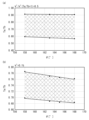
圧電薄膜共振器の周波数特性を有限要素法を用いシミュレーションした。シミュレーション条件は以下である。
圧電層14の厚さT:300nm
下部電極12:厚さが30nmのアルミニウム膜
上部電極16:厚さが30nmのアルミニウム膜
圧電層14bの厚さTbに対する圧電層14aの厚さTaをTa/Tbとした。Ta/Tb=1のとき、圧電層14aおよび14bの厚さTaおよびTbはいずれも150nmである。
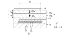
図10(a)から図10(c)は、実施例1の変形例1から3に係る圧電薄膜共振器の断面図である。図10(a)に示すように、実施例1の変形例1では、圧電層14aの分極方向52aが上方向であり、圧電層14bの分極方向52bが下方向である。その他の構成は実施例1と同じであり説明を省略する。
図10(b)に示すように、実施例1の変形例2では、圧電層14aの上面と圧電層14bの下面が接合されており、圧電層14aの下面に下部電極12が設けられ、圧電層14bの上面に上部電極16が設けられている。圧電層14aの分極方向52aは上方向であり、圧電層14bの分極方向52bは下方向である。その他の構成は実施例1と同じであり説明を省略する。
図10(c)に示すように、実施例1の変形例3では、圧電層14aの分極方向52aは下方向であり、圧電層14bの分極方向52bは上方向である。その他の構成は実施例1の変形例2と同じであり説明を省略する。
図11は、実施例1の変形例4に係る圧電薄膜共振器の断面図である。図11に示すように、実施例1の変形例4では、空隙34の代わりに、基板10と下部電極12との間に音響反射膜30が設けられている。音響反射膜30は、音響インピーダンスの低い膜31と音響インピーダンスの高い膜32とが交互に設けられている。膜31および32の膜厚は例えばそれぞれほぼλ/4(λは弾性波の波長)である。これにより、音響反射膜30は弾性波を反射する。膜31と膜32の積層数は任意に設定できる。音響反射膜30は共振領域50に重なり、音響反射膜30は共振領域50と同じ大きさまたは共振領域50より大きい。音響反射膜30の膜31は、例えば酸化シリコン、窒化シリコン等である。膜32は、例えばタングステン、タンタル、モリブデン、ルテニウム等である。
12 下部電極
14、14a、14b 圧電層
16 上部電極
30 音響反射膜
34 空隙
40 送信フィルタ
42 受信フィルタ
50 共振領域
52a、52b 分極方向
Claims (10)
- 回転Yカットタンタル酸リチウム基板であり、第1厚さを有する第1圧電層と、
回転Yカットニオブ酸リチウム基板であり、前記第1圧電層に積層され、前記第1厚さより小さい第2厚さを有し、前記第1圧電層の自発分極の方向と略反対方向の自発分極の方向を有する第2圧電層と、
前記第1圧電層の前記第2圧電層に対し反対の面に設けられた第1電極と、
前記第2圧電層の前記第1圧電層に対し反対の面に設けられ、前記第1電極とで前記第1圧電層の少なくとも一部および前記第2圧電層の少なくとも一部を挟む第2電極と、
を備える弾性波デバイス。 - 前記第1圧電層は、158°以上かつ168°以下回転Yカットタンタル酸リチウム基板であり、
前記第2圧電層は、158°以上かつ168°以下回転Yカットニオブ酸リチウム基板であり、
前記第2厚さは前記第1厚さの0.5倍以上である請求項1に記載の弾性波デバイス。 - 前記第2厚さは前記第1厚さの0.56倍以上かつ0.92倍以下である請求項2に記載の弾性波デバイス。
- 前記第2厚さは前記第1厚さの0.68倍以上かつ0.78倍以下である請求項2に記載の弾性波デバイス。
- 前記第1圧電層における回転Yカットタンタル酸リチウム基板の結晶方位のX軸方向と、前記第1圧電層における回転Yカットニオブ酸リチウム基板の結晶方位のX軸方向と、のなす角度は5°以下である請求項2から4のいずれか一項に記載の弾性波デバイス。
- 前記第1圧電層と前記第2圧電層とは直接接合されている請求項1から5のいずれか一項に記載の弾性波デバイス。
- 支持基板を備え、
前記第1圧電層は前記支持基板と前記第2圧電層との間に設けられている請求項1から6のいずれか一項に記載の弾性波デバイス。 - 支持基板を備え、
前記第2圧電層は前記支持基板と前記第1圧電層との間に設けられている請求項1から6のいずれか一項に記載の弾性波デバイス。 - 請求項1から8のいずれか一項に記載の弾性波デバイスを含むフィルタ。
- 請求項9に記載のフィルタを含むマルチプレクサ。
Priority Applications (2)
| Application Number | Priority Date | Filing Date | Title |
|---|---|---|---|
| JP2022027876A JP7785419B2 (ja) | 2022-02-25 | 2022-02-25 | 弾性波デバイス、フィルタおよびマルチプレクサ |
| US18/170,944 US12413204B2 (en) | 2022-02-25 | 2023-02-17 | Acoustic wave device, filter, and multiplexer |
Applications Claiming Priority (1)
| Application Number | Priority Date | Filing Date | Title |
|---|---|---|---|
| JP2022027876A JP7785419B2 (ja) | 2022-02-25 | 2022-02-25 | 弾性波デバイス、フィルタおよびマルチプレクサ |
Publications (2)
| Publication Number | Publication Date |
|---|---|
| JP2023124231A true JP2023124231A (ja) | 2023-09-06 |
| JP7785419B2 JP7785419B2 (ja) | 2025-12-15 |
Family
ID=87761308
Family Applications (1)
| Application Number | Title | Priority Date | Filing Date |
|---|---|---|---|
| JP2022027876A Active JP7785419B2 (ja) | 2022-02-25 | 2022-02-25 | 弾性波デバイス、フィルタおよびマルチプレクサ |
Country Status (2)
| Country | Link |
|---|---|
| US (1) | US12413204B2 (ja) |
| JP (1) | JP7785419B2 (ja) |
Cited By (2)
| Publication number | Priority date | Publication date | Assignee | Title |
|---|---|---|---|---|
| WO2025084367A1 (ja) * | 2023-10-17 | 2025-04-24 | 株式会社村田製作所 | 圧電デバイスおよびフィルタ |
| WO2026034248A1 (ja) * | 2024-08-09 | 2026-02-12 | 株式会社村田製作所 | 圧電デバイス |
Citations (5)
| Publication number | Priority date | Publication date | Assignee | Title |
|---|---|---|---|---|
| JPS63117507A (ja) * | 1986-11-05 | 1988-05-21 | Fujitsu Ltd | 圧電振動素子 |
| JPH0730354A (ja) * | 1993-07-14 | 1995-01-31 | Matsushita Electric Ind Co Ltd | 複合単結晶圧電基板の製造方法 |
| JPH07206600A (ja) * | 1994-01-24 | 1995-08-08 | Matsushita Electric Ind Co Ltd | 積層強誘電体及びその接合方法 |
| JPH1096742A (ja) * | 1995-10-09 | 1998-04-14 | Matsushita Electric Ind Co Ltd | 加速度センサ及びその製造方法、並びに加速度センサを利用した衝撃検知機器 |
| JP2021013133A (ja) * | 2019-07-09 | 2021-02-04 | 国立大学法人東北大学 | 振動子およびセンサ素子 |
Family Cites Families (8)
| Publication number | Priority date | Publication date | Assignee | Title |
|---|---|---|---|---|
| JPS5234196B2 (ja) | 1972-06-17 | 1977-09-01 | ||
| JP2958004B2 (ja) | 1986-09-02 | 1999-10-06 | 清水 郁子 | 分極反転領域を有するLiNbO▲下3▼基板を利用したデバイス |
| JPH03123214A (ja) | 1989-10-06 | 1991-05-27 | Fujitsu Ltd | 圧電振動子 |
| JPH07254836A (ja) | 1994-03-15 | 1995-10-03 | Matsushita Electric Ind Co Ltd | 圧電振動子 |
| JPH1051262A (ja) | 1996-04-16 | 1998-02-20 | Matsushita Electric Ind Co Ltd | 圧電振動子とその製造方法 |
| JP3859573B2 (ja) | 2002-10-21 | 2006-12-20 | 富士通メディアデバイス株式会社 | 弾性表面波フィルタ及びフィルタ装置 |
| US9065421B2 (en) * | 2012-01-31 | 2015-06-23 | Avago Technologies General Ip (Singapore) Pte. Ltd. | Film bulk acoustic resonator with multi-layers of different piezoelectric materials and method of making |
| US11595019B2 (en) * | 2018-04-20 | 2023-02-28 | Taiyo Yuden Co., Ltd. | Acoustic wave resonator, filter, and multiplexer |
-
2022
- 2022-02-25 JP JP2022027876A patent/JP7785419B2/ja active Active
-
2023
- 2023-02-17 US US18/170,944 patent/US12413204B2/en active Active
Patent Citations (5)
| Publication number | Priority date | Publication date | Assignee | Title |
|---|---|---|---|---|
| JPS63117507A (ja) * | 1986-11-05 | 1988-05-21 | Fujitsu Ltd | 圧電振動素子 |
| JPH0730354A (ja) * | 1993-07-14 | 1995-01-31 | Matsushita Electric Ind Co Ltd | 複合単結晶圧電基板の製造方法 |
| JPH07206600A (ja) * | 1994-01-24 | 1995-08-08 | Matsushita Electric Ind Co Ltd | 積層強誘電体及びその接合方法 |
| JPH1096742A (ja) * | 1995-10-09 | 1998-04-14 | Matsushita Electric Ind Co Ltd | 加速度センサ及びその製造方法、並びに加速度センサを利用した衝撃検知機器 |
| JP2021013133A (ja) * | 2019-07-09 | 2021-02-04 | 国立大学法人東北大学 | 振動子およびセンサ素子 |
Cited By (2)
| Publication number | Priority date | Publication date | Assignee | Title |
|---|---|---|---|---|
| WO2025084367A1 (ja) * | 2023-10-17 | 2025-04-24 | 株式会社村田製作所 | 圧電デバイスおよびフィルタ |
| WO2026034248A1 (ja) * | 2024-08-09 | 2026-02-12 | 株式会社村田製作所 | 圧電デバイス |
Also Published As
| Publication number | Publication date |
|---|---|
| JP7785419B2 (ja) | 2025-12-15 |
| US20230275566A1 (en) | 2023-08-31 |
| US12413204B2 (en) | 2025-09-09 |
Similar Documents
| Publication | Publication Date | Title |
|---|---|---|
| US11469735B2 (en) | Acoustic wave device, filter, and multiplexer | |
| JP7261568B2 (ja) | 弾性波デバイス、フィルタおよびマルチプレクサ | |
| CN113411070B (zh) | 弹性波器件和滤波器 | |
| JP7456734B2 (ja) | 弾性波デバイス、フィルタおよびマルチプレクサ | |
| US12413204B2 (en) | Acoustic wave device, filter, and multiplexer | |
| WO2022249926A1 (ja) | 圧電バルク波装置及びその製造方法 | |
| WO2022230723A1 (ja) | 弾性波装置 | |
| JP2020141337A (ja) | 圧電薄膜共振器、フィルタおよびマルチプレクサ | |
| WO2023224072A1 (ja) | 弾性波装置 | |
| JP7807927B2 (ja) | 圧電薄膜共振器、フィルタおよびマルチプレクサ | |
| JP2020027987A (ja) | 圧電薄膜共振器、フィルタおよびマルチプレクサ | |
| WO2024034603A1 (ja) | 弾性波装置 | |
| WO2023002822A1 (ja) | 弾性波装置及びその製造方法 | |
| JP7825345B2 (ja) | 弾性波デバイス、フィルタ、マルチプレクサ、および弾性波デバイスの製造方法 | |
| JP7829370B2 (ja) | 弾性波デバイス、フィルタ、およびマルチプレクサ | |
| JP7853837B2 (ja) | 弾性波デバイス、フィルタおよびマルチプレクサ | |
| JP2024140687A (ja) | 弾性波デバイス、フィルタ、およびマルチプレクサ | |
| US12255602B2 (en) | Filter and multiplexer | |
| WO2023013741A1 (ja) | 弾性波装置 | |
| JP7850509B2 (ja) | フィルタおよびマルチプレクサ | |
| JP2025123945A (ja) | 弾性波デバイス、フィルタ、マルチプレクサ、及び弾性波デバイスの製造方法 | |
| JP2024025031A (ja) | 弾性波デバイス、フィルタ、およびマルチプレクサ | |
| JP2024120503A (ja) | フィルタ、マルチプレクサ、およびフィルタの製造方法 | |
| JP2025123946A (ja) | 弾性波デバイス、フィルタ、マルチプレクサ、及び弾性波デバイスの製造方法 | |
| JP2024142158A (ja) | 弾性波デバイス、フィルタ、およびマルチプレクサ |
Legal Events
| Date | Code | Title | Description |
|---|---|---|---|
| A521 | Request for written amendment filed |
Free format text: JAPANESE INTERMEDIATE CODE: A523 Effective date: 20230327 |
|
| A621 | Written request for application examination |
Free format text: JAPANESE INTERMEDIATE CODE: A621 Effective date: 20250221 |
|
| TRDD | Decision of grant or rejection written | ||
| A977 | Report on retrieval |
Free format text: JAPANESE INTERMEDIATE CODE: A971007 Effective date: 20251120 |
|
| A01 | Written decision to grant a patent or to grant a registration (utility model) |
Free format text: JAPANESE INTERMEDIATE CODE: A01 Effective date: 20251125 |
|
| RD02 | Notification of acceptance of power of attorney |
Free format text: JAPANESE INTERMEDIATE CODE: A7422 Effective date: 20251201 |
|
| RD04 | Notification of resignation of power of attorney |
Free format text: JAPANESE INTERMEDIATE CODE: A7424 Effective date: 20251201 |
|
| A61 | First payment of annual fees (during grant procedure) |
Free format text: JAPANESE INTERMEDIATE CODE: A61 Effective date: 20251201 |
|
| R150 | Certificate of patent or registration of utility model |
Ref document number: 7785419 Country of ref document: JP Free format text: JAPANESE INTERMEDIATE CODE: R150 |