JP3147868U - Substrate processing equipment - Google Patents
Substrate processing equipment Download PDFInfo
- Publication number
- JP3147868U JP3147868U JP2008007771U JP2008007771U JP3147868U JP 3147868 U JP3147868 U JP 3147868U JP 2008007771 U JP2008007771 U JP 2008007771U JP 2008007771 U JP2008007771 U JP 2008007771U JP 3147868 U JP3147868 U JP 3147868U
- Authority
- JP
- Japan
- Prior art keywords
- reactor
- gas
- shower plate
- substrate processing
- processing apparatus
- Prior art date
- Legal status (The legal status is an assumption and is not a legal conclusion. Google has not performed a legal analysis and makes no representation as to the accuracy of the status listed.)
- Expired - Lifetime
Links
Images



Landscapes
- Chemical Vapour Deposition (AREA)
Abstract
【課題】リアクタのクリーニング時間を短縮し、生産性の高い基板処理装置を提供する。【解決手段】基板処理装置は、リアクタと、被処理体を載置するためのサセプタと、サセプタと対向して平行に配置されたシャワープレートと、リアクタから離隔して設けられた遠隔プラズマチャンバと、遠隔プラズマチャンバと、リアクタとを連結するガス導入管とを備え、遠隔プラズマチャンバ内で、クリーニングガスが活性化され、シャワープレートは、ガス導入面とガス噴射面を有し、ガス噴射面は膜被覆処理されているが、ガス導入面は膜被覆処理されていないことを特徴とする。【選択図】図2The present invention provides a highly productive substrate processing apparatus that shortens the cleaning time of a reactor. A substrate processing apparatus includes a reactor, a susceptor for placing an object to be processed, a shower plate arranged in parallel to face the susceptor, and a remote plasma chamber provided apart from the reactor. A remote plasma chamber and a gas introduction pipe connecting the reactor, the cleaning gas is activated in the remote plasma chamber, the shower plate has a gas introduction surface and a gas injection surface, Although the film coating process is performed, the gas introduction surface is not subjected to the film coating process. [Selection] Figure 2
Description
本考案は、基板処理装置の構造に関し、特に、反応室内部をクリーニングする装置の構造に関する。 The present invention relates to the structure of a substrate processing apparatus, and more particularly to the structure of an apparatus for cleaning the inside of a reaction chamber.
従来、被処理体上に薄膜を形成若しくは除去するために、または被処理体の表面を改質するために、プラズマ処理装置が使用されてきた。特に、シリコンなどの半導体ウエハ及びガラス基板上への薄膜の形成若しくはエッチング処理は、メモリ若しくはCPUなどの半導体素子、または液晶ディスプレイ(LCD)の製作に不可欠な基本的技術となっている。 Conventionally, a plasma processing apparatus has been used to form or remove a thin film on an object to be processed, or to modify the surface of the object to be processed. In particular, the formation or etching process of a thin film on a semiconductor wafer such as silicon and a glass substrate has become a basic technique indispensable for manufacturing a semiconductor element such as a memory or a CPU, or a liquid crystal display (LCD).
プラズマCVD法は、真空排気された反応容器内に各種原料ガスを導入し、高周波電力を印加することで、プラズマを発生させ、ウエハ上にさまざまな薄膜を堆積する処理方法である。プラズマCVD処理装置は、概して、リアクタと、反応ガスを均等に分配するガス分散板を兼ねる上部高周波電極(シャワープレート)と、ウエハを保持するためのサセプタを兼ねる下部高周波電極とを備える。該リアクタは、ゲートバルブを介して搬送室と結合されている。該搬送室の内部にはウエハをリアクタ内へ搬入若しくは搬出するための搬送ロボットが設置されている。 The plasma CVD method is a processing method in which various raw material gases are introduced into a vacuum evacuated reaction vessel and high frequency power is applied to generate plasma and deposit various thin films on a wafer. The plasma CVD processing apparatus generally includes a reactor, an upper high-frequency electrode (shower plate) that also serves as a gas dispersion plate that evenly distributes reaction gas, and a lower high-frequency electrode that also serves as a susceptor for holding a wafer. The reactor is coupled to the transfer chamber via a gate valve. Inside the transfer chamber, a transfer robot for carrying wafers into and out of the reactor is installed.
リアクタ内の反応領域においてプラズマ励起により活性化された原料ガスのイオン種が半導体基板表面近傍において化学反応を起こし、該半導体基板上に薄膜が堆積される。この際、リアクタの内壁及びサセプタのようなウエハ支持体表面にも薄膜が付着する。これらの不所望な付着物質は、薄膜形成処理が繰り返されるたびに蓄積し、最後には、リアクタ内壁及びサセプタ表面から剥離してリアクタ内を浮遊する汚染物質となる。この汚染物質は、製造段階において半導体回路に欠陥を生じさせ、結果として、歩留まりの低下を引き起こす。 The ion species of the source gas activated by plasma excitation in the reaction region in the reactor cause a chemical reaction in the vicinity of the surface of the semiconductor substrate, and a thin film is deposited on the semiconductor substrate. At this time, the thin film also adheres to the inner wall of the reactor and the surface of the wafer support such as the susceptor. These undesired deposits accumulate each time the thin film formation process is repeated, and eventually become contaminants that peel off the reactor inner wall and susceptor surface and float in the reactor. This contaminant causes defects in the semiconductor circuit during the manufacturing stage, resulting in a decrease in yield.
この問題を解決するために、リアクタ内部を定期的にクリーニングする方法がある。例えば、リアクタ内壁に付着した汚染物質を除去するために、クリーニングガスをリアクタ内部に導入し、該汚染物質を気体材料に分離することにより除去する方法がある。そのひとつの方法として、ここに参考文献として組み込む米国特許第5,788,778号及び米国特許第5,844,195号には、NF3をクリーニングガスとして使用し、リアクタから離隔された第2プラズマ放電チャンバ内でマイクロ波を使ったプラズマ励起によりNF3を活性化させる、遠隔プラズマクリーニング方法が開示されている。この方法によれば、流量制御されたNF3が第2プラズマ放電チャンバ内に導入され、それは導波管を通じてマイクロ波オシレータから第2プラズマ放電チャンバに印加される2.45GHzのマイクロ波によって解離されかつ活性化され、フッ素活性種が生成される。マイクロ波プラズマ放電を効率的に達成するために、第2プラズマ放電チャンバとリアクタとの間には圧力調整用のバルブが設けられ、第2プラズマ放電チャンバ内部の圧力は指定された圧力に維持される。こうして生成されたフッ素活性種は導管を通じてリアクタ内に導入され、リアクタ内壁及びサセプタ上に付着した汚染物質を分解しかつ除去する。 In order to solve this problem, there is a method of periodically cleaning the inside of the reactor. For example, in order to remove contaminants attached to the inner wall of the reactor, there is a method of removing the contaminants by introducing a cleaning gas into the reactor and separating the contaminants into gaseous materials. As one method, U.S. Pat. No. 5,788,778 and U.S. Pat. No. 5,844,195, which are incorporated herein by reference, use a second plasma separated from the reactor using NF3 as a cleaning gas. A remote plasma cleaning method is disclosed in which NF3 is activated by plasma excitation using microwaves in a discharge chamber. According to this method, flow-controlled NF3 is introduced into the second plasma discharge chamber, which is dissociated by the 2.45 GHz microwave applied from the microwave oscillator to the second plasma discharge chamber through the waveguide and Activated to produce fluorine active species. In order to efficiently achieve microwave plasma discharge, a pressure regulating valve is provided between the second plasma discharge chamber and the reactor, and the pressure inside the second plasma discharge chamber is maintained at a specified pressure. The The fluorine active species thus generated is introduced into the reactor through a conduit, and decomposes and removes contaminants deposited on the reactor inner wall and the susceptor.
しかしながら、従来の上記方法では、フッ素活性種をリアクタ内に導入する過程で、フッ素活性種が途中の配管、リアクタ内部のシャワープレート等の構成部品と反応してしまうため、最終的にリアクタ内に導入されるフッ素活性種の量が生成当初に比べ減少する。その結果、リアクタのクリーニング時間が増加し、装置の生産性が低下するという問題がある。
本願の目的は、リアクタのクリーニング時間を短縮し、生産性の高い基板処理装置を提供することである。 An object of the present application is to provide a highly productive substrate processing apparatus that shortens the cleaning time of the reactor.
本考案のひとつの態様において、基板処理装置は、
リアクタと、
前記リアクタ内部に設けられた被処理体を載置するためのサセプタと、
前記リアクタの内部にあって、前記サセプタと対向して平行に配置され、ガスを前記被処理体に向けて噴射するための複数の細孔を有するシャワープレートと、
前記リアクタから離隔して設けられた遠隔プラズマチャンバと、
前記遠隔プラズマチャンバと、前記リアクタとを連結するガス導入管と、
を備え、
前記遠隔プラズマチャンバ内で、クリーニングガスが活性化され、
前記シャワープレートは、ガスが前記ガス導入管を通じて導入されるガス導入面と、前記複数の細孔を通じて前記ガスを前記被処理体の表面に噴射するガス噴射面を有し、前記ガス噴射面は表面加工処理されているが、前記ガス導入面は表面加工処理されていないことを特徴とする。
In one aspect of the present invention, the substrate processing apparatus comprises:
A reactor,
A susceptor for placing an object to be processed provided in the reactor;
A shower plate inside the reactor, disposed in parallel to face the susceptor, and having a plurality of pores for injecting a gas toward the object to be processed;
A remote plasma chamber provided remotely from the reactor;
A gas introduction pipe connecting the remote plasma chamber and the reactor;
With
Within the remote plasma chamber, a cleaning gas is activated,
The shower plate has a gas introduction surface through which gas is introduced through the gas introduction pipe, and a gas injection surface for injecting the gas onto the surface of the object to be processed through the plurality of pores. Although the surface treatment is performed, the gas introduction surface is not surface-treated.
本願によれば、リアクタのクリーニング時間が短縮し、生産性の高い基板処理装置を提供することができる。 According to the present application, the time required for cleaning the reactor can be shortened, and a highly productive substrate processing apparatus can be provided.
以下、図面を参照しながら、本考案の実施形態について説明する。 Hereinafter, embodiments of the present invention will be described with reference to the drawings.
[考案の第1の実施形態]
図1は、本考案の第1の実施形態に係る半導体処理装置を概略的に示したものである。第1の実施形態に係る半導体処理装置1は、リアクタ2と、該リアクタ2の内部に設置され半導体基板3を支持するためのサセプタ4と、リアクタ2内部にあって、該サセプタ4と対向しそれと平行に配置されたシャワープレート5と、リアクタから離隔して配置された遠隔プラズマチャンバ6とを備えて構成されている。
[First embodiment of the invention]
FIG. 1 schematically shows a semiconductor processing apparatus according to a first embodiment of the present invention. The
サセプタ4は、例えば抵抗加熱型ヒータ(図示せず)を埋設しており、半導体基板3を所望の温度に加熱保持する。また、サセプタ4は昇降機構7と結合されており、垂直方向に上下移動することが可能である。さらに、半導体処理装置がプラズマCVD装置の場合には、サセプタ4は電気的に接地8されており、プラズマ放電のための一方の電極を画成する。
The susceptor 4 embeds, for example, a resistance heater (not shown), and heats and holds the semiconductor substrate 3 at a desired temperature. Further, the susceptor 4 is coupled to the
リアクタ2には、ゲートバルブ9を介して、搬送室(図示せず)が結合されている。また、リアクタ2の底部には、排気口10が設けられており、該排気口10は、コンダクタンス調整バルブ11を介して真空排気ポンプ(図示せず)に結合され、リアクタ2内部が所望の圧力に制御される。
A transfer chamber (not shown) is coupled to the
シャワープレート5は、ガスを半導体基板3に対して均一に噴射するための複数の細孔(図2参照)を有する。シャワープレートの上部にはガス導入口19が設けられ、該ガス導入口19は、ガス導入管12を通じて遠隔プラズマチャンバ6と結合されている。ガス導入管12には配管13が結合され、該配管13はソースガス供給装置(図示せず)と結合されている。半導体処理装置1がプラズマCVD装置の場合には、シャワープレート5は、高周波発振器14(例えば、13.56MHz)と出力ケーブル15を介して電気的に接続されており、プラズマ放電のもう一方の電極を画成する。付加的に、高周波発振器14とシャワープレート5の間には、整合回路16が設けられてもよい。
The shower plate 5 has a plurality of pores (see FIG. 2) for injecting gas uniformly to the semiconductor substrate 3. A
遠隔プラズマチャンバ6は、例えば2.45GHzのマイクロ波を生成するマイクロ波オシレータ(図示せず)と接続している。遠隔プラズマチャンバ6には配管17が結合されており、該配管17を通じて、例えば、NF3のようなクリーニングガスが供給される。ガス導入管12にはバルブ18が設けられている。
The
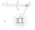
本考案の第1の実施形態に従う基板処理装置のシャワープレート5を図2に示す。図2(a)は、シャワープレート5の断面図であり、図2(b)は、シャワープレート5の部分拡大断面図である。図1と同じ構成要素については同一符号で示す。 The shower plate 5 of the substrate processing apparatus according to the first embodiment of the present invention is shown in FIG. FIG. 2A is a sectional view of the shower plate 5, and FIG. 2B is a partial enlarged sectional view of the shower plate 5. The same components as those in FIG. 1 are denoted by the same reference numerals.
本考案の第1の実施形態に従う基板処理装置のシャワープレート5は、上部のガス導入面21、下部のガス噴射面22、及びガス導入面21とガス噴射面22との間を貫通する約数百から数千個の細孔23を有する。シャワープレート5は、例えば、アルミニウムやアルミニウム合金から研磨または研削により作製されるが、それ以外の金属、セラミック等から作製されてよい。
The shower plate 5 of the substrate processing apparatus according to the first embodiment of the present invention has an upper
図2(b)に示すように、本考案の第1の実施形態において、シャワープレート5のガス噴射面22には、例えば、陽極酸化膜処理24が施されている。同様に、細孔23の側面にも陽極酸化膜処理25が施されている。一方、ガス導入面21には陽極酸化膜処理が施されていない。本考案の第1の実施形態において、シャワープレート5をこのように構成することにより、活性種の損失を防止することができ、生産性の高い基板処理装置を与えることができる。以下、この点について詳細に説明する。
As shown in FIG. 2B, in the first embodiment of the present invention, for example, an anodic
元来、陽極酸化膜は、シャワープレートを構成するアルミニウムまたはアルミニウム合金を、プラズマ反応に伴う腐食やスパッタリングから保護するためにシャワープレートに対して施されるものである。しかし、クリーニング活性種の活性を奪うという側面もある。 Originally, the anodic oxide film is applied to the shower plate in order to protect the aluminum or aluminum alloy constituting the shower plate from corrosion and sputtering accompanying the plasma reaction. However, there is also an aspect of depriving the activity of the cleaning active species.
本願の考案者らは、この点に知見を得たものである。すなわち、シャワープレート5のガス噴射面側にのみ陽極酸化膜処理を施すことにより、プラズマ反応に伴う腐食やスパッタリングを防止すると同時に、ガス導入面側を陽極酸化膜処理しないことで、クリーニング活性種の失活を最小限にすることができることを見いだしたのである。 The inventors of the present application have obtained knowledge on this point. That is, by performing the anodic oxide film treatment only on the gas injection surface side of the shower plate 5, corrosion and sputtering associated with the plasma reaction are prevented, and at the same time, the gas introduction surface side is not subjected to the anodic oxide film treatment. They found that deactivation could be minimized.
シャワープレートのクリーニング速度を向上させるために、シャワープレートの温度を高温に保持することが有効である。シャワープレート5は、サセプタ4からの輻射熱により加熱され、ガス噴射面に施された陽極酸化膜が赤外線を吸収し、シャワープレート5を高温に保持する作用を有する。また、付加的に、リアクタ上面にシャワープレート用のヒータまたは温度調節機器を設けてもよい。 In order to improve the cleaning speed of the shower plate, it is effective to keep the temperature of the shower plate at a high temperature. The shower plate 5 is heated by the radiant heat from the susceptor 4, and the anodic oxide film applied to the gas injection surface absorbs infrared rays and has an action of keeping the shower plate 5 at a high temperature. In addition, a heater for a shower plate or a temperature control device may be provided on the upper surface of the reactor.
次に、本考案の第1の実施形態に係るシャワープレートの作製方法について説明する。 Next, a method for producing a shower plate according to the first embodiment of the present invention will be described.
まず、アルミニウムまたはアルミニウム合金から、周知の研磨、研削技術等を用いて機械加工することによりシャワープレートを作製する。 First, a shower plate is produced from aluminum or an aluminum alloy by machining using a known polishing or grinding technique.
次に、作製したシャワープレートを寸法検査した後、不純物を除去するために脱脂洗浄する。 Next, after dimensional inspection of the produced shower plate, degreasing cleaning is performed to remove impurities.
続いて、シャワープレートのガス導入面に対して陽極酸化膜形成防止用のマスキングを行う。 Subsequently, masking for preventing the formation of the anodized film is performed on the gas introduction surface of the shower plate.
次いで、シャワープレート表面の自然酸化膜または不純物を除去する前処理工程を経て、シャワープレート全体を陽極酸化処理する。その後、後処理として洗浄工程が実行し薬液を除去する。 Next, the entire shower plate is anodized through a pretreatment process for removing the natural oxide film or impurities on the surface of the shower plate. Thereafter, a cleaning process is performed as a post-treatment to remove the chemical solution.
最後に、ガス導入面のマスキングを取り除き、陽極酸化膜の検査を行う。付加的に、マスクを除去した後、ガス導入面を少なくとも化学的若しくは機械的研磨の一方の処理を施すことにより平坦加工してもよい。さらに、ガス導入面に対してフッ化不動態処理を施してもよい。 Finally, the masking of the gas introduction surface is removed and the anodic oxide film is inspected. In addition, after removing the mask, the gas introduction surface may be flattened by performing at least one of chemical and mechanical polishing. Further, a fluorination passivation treatment may be performed on the gas introduction surface.
次に、本考案の第1の実施形態に係る基板処理装置の動作について詳細に説明する。 Next, the operation of the substrate processing apparatus according to the first embodiment of the present invention will be described in detail.
まず、ゲートバルブ9を介して処理済みの半導体基板3を搬出した後、ゲートバルブを閉じてリアクタ2内部を真空排気した後、配管13に設けられたバルブ(図示せず)を閉じる。
First, after the processed semiconductor substrate 3 is unloaded through the
次に、バルブ18を開き、配管17を通じて、例えばNF3のようなクリーニングガスを遠隔プラズマチャンバ6に供給する。
Next, the
続いて、遠隔プラズマチャンバ6に、2.45GHzのマイクロ波を印加し、クリーニングガスを解離し、活性化してフッ素活性種を生成し、ガス導入管12を通じてシャワープレート5に導入する。
Subsequently, a microwave of 2.45 GHz is applied to the
最後に、シャワープレート5の細孔23からフッ素活性種がリアクタ2内部に導入され、リアクタ2の内壁またはサセプタ4の表面等に付着した堆積物を気体材料に分解し、排気口10から排気する。
Finally, fluorine active species are introduced into the
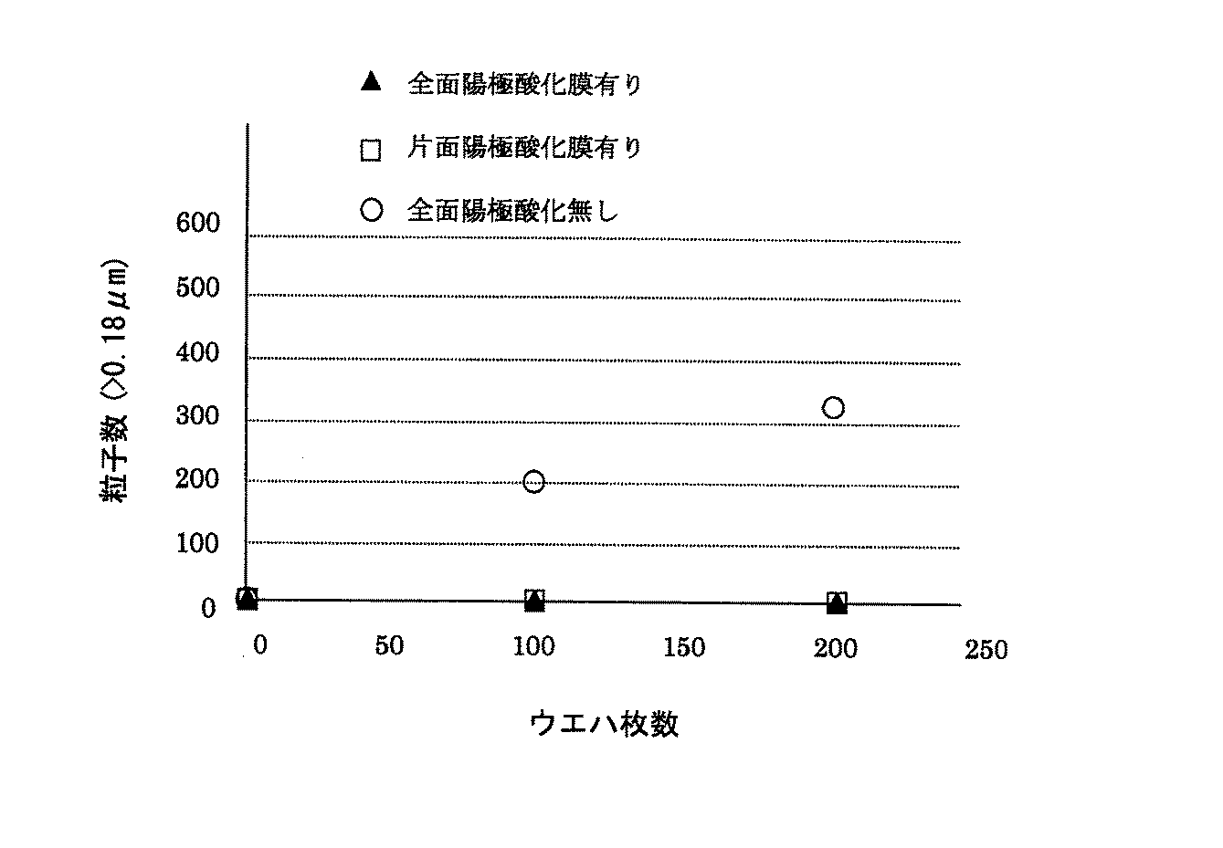
シャワープレート全面に陽極酸化膜処理を施した比較例1、シャワープレート全面に陽極酸化膜処理を施さなかった比較例2、及び本考案の第1の実施形態に係る片面にのみ陽極酸化膜処理を施した実施例について、リアクタクリーニング速度を測定する実験及びウエハ処理枚数とウエハ上のパーティクル数の関係を調べる実験を行ったので説明する。 Comparative Example 1 in which the entire surface of the shower plate was subjected to anodic oxide film processing, Comparative Example 2 in which the entire surface of the shower plate was not subjected to anodic oxide film processing, and anodic oxide film processing only on one side according to the first embodiment of the present invention The applied example will be described because an experiment for measuring the reactor cleaning speed and an experiment for examining the relationship between the number of processed wafers and the number of particles on the wafer were performed.
表1は、比較例1、比較例2、及び実施例について、リアクタクリーニング速度(nm/min)を比較したものである。図3に比較例1のシャワープレートを示す。図3(a)は、比較例1の従来のシャワープレートの断面図であり、図3(b)はその部分拡大断面図である。図2と同じ構成要素については、同一符号で示す。図3(b)に示すように、従来のシャワープレートでは、ガス導入面21に陽極酸化膜31、ガス噴射面22に陽極酸化膜24が施されている。
Table 1 compares the reactor cleaning rate (nm / min) for Comparative Example 1, Comparative Example 2, and Example. FIG. 3 shows the shower plate of Comparative Example 1. 3A is a cross-sectional view of a conventional shower plate of Comparative Example 1, and FIG. 3B is a partially enlarged cross-sectional view thereof. The same components as those in FIG. 2 are denoted by the same reference numerals. As shown in FIG. 3B, in the conventional shower plate, an
また、比較例1と実施例とを対比すると、片面のみに陽極酸化膜処理を施した実施例の方がクリーニング速度が大幅に向上していることがわかる。この結果より、本考案の第1の実施形態に係るシャワープレートは、クリーニング活性種の失活を十分に抑制することができることが立証された。 Further, when Comparative Example 1 is compared with the Example, it can be seen that the cleaning rate is greatly improved in the Example in which the anodic oxide film treatment is performed only on one side. From this result, it was proved that the shower plate according to the first embodiment of the present invention can sufficiently suppress the deactivation of the cleaning active species.
図4は、上記した比較例1、比較例2及び実施例に対する、ウエハ処理枚数とウエハ上のパーティクル数の関係を示したグラフである。本考案の第1の実施形態に係るシャワープレートによれば、ウエハ処理枚数が増加しても、パーティクル数の増加は見られず、汚染物質を抑制する効果が十分に得られることが立証された。 FIG. 4 is a graph showing the relationship between the number of wafers processed and the number of particles on the wafer for Comparative Example 1, Comparative Example 2 and Examples described above. According to the shower plate according to the first embodiment of the present invention, even when the number of wafers processed increases, the number of particles does not increase, and it has been proved that the effect of suppressing contaminants can be sufficiently obtained. .
本考案の第1実施形態によれば、クリーニング活性種の失活を抑制し、リアクタクリーニング速度の向上及び安定したプロセス性能を提供することができる。結果として、クリーニングに要するガス量の低減及びクリーニング時間の短縮による生産性の向上を図ることが可能となる。 According to the first embodiment of the present invention, it is possible to suppress the deactivation of cleaning active species, improve the reactor cleaning speed, and provide stable process performance. As a result, it is possible to improve productivity by reducing the amount of gas required for cleaning and shortening the cleaning time.
[考案の第2の実施形態]
次に、本考案の第2の実施形態に係る基板処理装置について説明する。第2実施形態に係る基板処理装置は、シャワープレートの細孔23の側面に陽極酸化膜が施されていない点で、第1実施形態と異なる。
[Second Embodiment of the Invention]
Next, a substrate processing apparatus according to a second embodiment of the present invention will be described. The substrate processing apparatus according to the second embodiment is different from the first embodiment in that an anodic oxide film is not provided on the side surfaces of the
その他の構成及び動作については、第1実施形態と同様なので説明を省略する。 Since other configurations and operations are the same as those in the first embodiment, the description thereof is omitted.
本考案の第2実施形態によれば、クリーニング活性種の失活をさらに抑制し、リアクタクリーニング速度の向上及び安定したプロセス性能を提供することができる。結果として、クリーニングに要するガス量の低減及びクリーニング時間のさらなる短縮による生産性の向上を図ることが可能となる。 According to the second embodiment of the present invention, the deactivation of cleaning active species can be further suppressed, and the reactor cleaning speed can be improved and stable process performance can be provided. As a result, it is possible to improve productivity by reducing the amount of gas required for cleaning and further shortening the cleaning time.
[その他]
以上、本考案の特定の実施形態について説明してきたが、ここに開示される装置の構造は例示に過ぎず、実用新案登録請求の範囲に記載された本考案の思想から離れることなく、さまざまな修正及び変更が可能であることは当業者の知るところである。
[Others]
Although specific embodiments of the present invention have been described above, the structure of the apparatus disclosed herein is merely an example, and various configurations can be made without departing from the spirit of the present invention described in the claims of the utility model registration. Those skilled in the art know that modifications and changes are possible.
例えば、本考案の実施形態は、プラズマCVD装置に関連して説明してきたが、熱CVD装置、原子層堆積装置(ALD)、プラズマ強化原子層堆積装置(PE−ALD)、物理的気相成長装置(PVD)についても同様に適用可能である。また、陽極酸化膜だけでなく、同様の機能を有するコーティング膜についても本考案を適用可能であることは言うまでもない。 For example, although embodiments of the present invention have been described with reference to plasma CVD apparatus, thermal CVD apparatus, atomic layer deposition apparatus (ALD), plasma enhanced atomic layer deposition apparatus (PE-ALD), physical vapor deposition The same applies to the apparatus (PVD). Needless to say, the present invention can be applied not only to the anodic oxide film but also to a coating film having a similar function.
1・・・半導体製造装置、2・・・リアクタ、3・・・半導体基板、4・・・サセプタ、5・・・シャワープレート、6・・・遠隔プラズマチャンバ、7・・・昇降装置、8・・・接地、9・・・ゲートバルブ、10・・・排気口、11・・・コンダクタンス調整弁、12・・・ガス導入管、13・・・配管、14・・・高周波発振器、15・・・出力ケーブル、16・・・整合回路、17・・・配管、18・・・バルブ、19・・・ガス導入口、21・・・ガス導入面、22・・・ガス噴射面、23・・・細孔、24・・・陽極酸化膜、25・・・陽極酸化膜。
DESCRIPTION OF
Claims (5)
前記リアクタ内部に設けられた被処理体を載置するためのサセプタと、
前記リアクタの内部にあって、前記サセプタと対向して平行に配置され、ガスを前記被処理体に向けて噴射するための複数の細孔を有するシャワープレートと、
前記リアクタから離隔して設けられた遠隔プラズマチャンバと、
前記遠隔プラズマチャンバと、前記リアクタとを連結するガス導入管と、
を備え、
前記遠隔プラズマチャンバ内で、クリーニングガスが活性化され、
前記シャワープレートは、ガスが前記ガス導入管を通じて導入されるガス導入面と、前記複数の細孔を通じて前記ガスを前記被処理体の表面に噴射するガス噴射面を有し、前記ガス噴射面は膜被覆処理されているが、前記ガス導入面は膜被覆処理されていないことを特徴とする、
基板処理装置。 A reactor,
A susceptor for placing an object to be processed provided in the reactor;
A shower plate inside the reactor, disposed in parallel to face the susceptor, and having a plurality of pores for injecting a gas toward the object to be processed;
A remote plasma chamber provided remotely from the reactor;
A gas introduction pipe connecting the remote plasma chamber and the reactor;
With
Within the remote plasma chamber, a cleaning gas is activated,
The shower plate has a gas introduction surface through which gas is introduced through the gas introduction pipe, and a gas injection surface for injecting the gas onto the surface of the object to be processed through the plurality of pores. Although the film coating process is performed, the gas introduction surface is not subjected to a film coating process.
Substrate processing equipment.
Priority Applications (1)
| Application Number | Priority Date | Filing Date | Title |
|---|---|---|---|
| JP2008007771U JP3147868U (en) | 2008-11-06 | 2008-11-06 | Substrate processing equipment |
Applications Claiming Priority (1)
| Application Number | Priority Date | Filing Date | Title |
|---|---|---|---|
| JP2008007771U JP3147868U (en) | 2008-11-06 | 2008-11-06 | Substrate processing equipment |
Publications (1)
| Publication Number | Publication Date |
|---|---|
| JP3147868U true JP3147868U (en) | 2009-01-22 |
Family
ID=54781470
Family Applications (1)
| Application Number | Title | Priority Date | Filing Date |
|---|---|---|---|
| JP2008007771U Expired - Lifetime JP3147868U (en) | 2008-11-06 | 2008-11-06 | Substrate processing equipment |
Country Status (1)
| Country | Link |
|---|---|
| JP (1) | JP3147868U (en) |
Cited By (4)
| Publication number | Priority date | Publication date | Assignee | Title |
|---|---|---|---|---|
| JP2016051864A (en) * | 2014-09-02 | 2016-04-11 | 株式会社日立国際電気 | Semiconductor device manufacturing method, substrate processing apparatus, and program |
| CN115440562A (en) * | 2021-06-02 | 2022-12-06 | 东京毅力科创株式会社 | Showerheads, electrode assemblies, gas supply assemblies, substrate processing devices and systems |
| CN118140008A (en) * | 2021-09-17 | 2024-06-04 | 应用材料公司 | One side of the diffuser is anodized |
| CN118186368A (en) * | 2024-03-15 | 2024-06-14 | 江苏微导纳米科技股份有限公司 | Reaction equipment, semiconductor coating equipment and cleaning method for reaction equipment |
-
2008
- 2008-11-06 JP JP2008007771U patent/JP3147868U/en not_active Expired - Lifetime
Cited By (7)
| Publication number | Priority date | Publication date | Assignee | Title |
|---|---|---|---|---|
| JP2016051864A (en) * | 2014-09-02 | 2016-04-11 | 株式会社日立国際電気 | Semiconductor device manufacturing method, substrate processing apparatus, and program |
| US9640387B2 (en) | 2014-09-02 | 2017-05-02 | Hitachi Kokusai Electric Inc. | Method of manufacturing semiconductor device, substrate processing apparatus, and recording medium |
| CN115440562A (en) * | 2021-06-02 | 2022-12-06 | 东京毅力科创株式会社 | Showerheads, electrode assemblies, gas supply assemblies, substrate processing devices and systems |
| CN118140008A (en) * | 2021-09-17 | 2024-06-04 | 应用材料公司 | One side of the diffuser is anodized |
| JP2024535234A (en) * | 2021-09-17 | 2024-09-30 | アプライド マテリアルズ インコーポレイテッド | Single-sided anodizing of the diffuser |
| JP7807533B2 (en) | 2021-09-17 | 2026-01-27 | アプライド マテリアルズ インコーポレイテッド | Single-sided anodizing of the diffuser |
| CN118186368A (en) * | 2024-03-15 | 2024-06-14 | 江苏微导纳米科技股份有限公司 | Reaction equipment, semiconductor coating equipment and cleaning method for reaction equipment |
Similar Documents
| Publication | Publication Date | Title |
|---|---|---|
| JP7079686B2 (en) | Film formation method and film formation equipment | |
| CN109075030B (en) | Plasma processing process for in-situ chamber cleaning efficiency enhancement in a plasma processing chamber | |
| KR100729900B1 (en) | Substrate processing apparatus having surface-treated showerhead and cleaning method of substrate processing apparatus | |
| KR100447284B1 (en) | Method of cleaning chemical vapor deposition chamber | |
| CN112640041B (en) | Method for removing SnO2 film from chamber | |
| KR100654121B1 (en) | Method for removing a deposited film | |
| KR102007019B1 (en) | Aluminum fluoride mitigation by plasma treatment | |
| JP2001274105A (en) | Semiconductor processing apparatus with remote plasma source for self-cleaning | |
| WO2014179087A1 (en) | Cobalt removal for chamber clean or pre-clean process | |
| US20060090773A1 (en) | Sulfur hexafluoride remote plasma source clean | |
| KR20010039780A (en) | A hot element cvd apparatus and a method for removing a deposited film | |
| TW201909272A (en) | Cleaning method of plasma processing device | |
| JP2000323467A (en) | Semiconductor processing apparatus having remote plasma discharge chamber | |
| KR102890186B1 (en) | Methods for coating slit valve gates and cleaning slit valve gates | |
| CN100549226C (en) | Cleaning methods for chemical vapor deposition equipment | |
| US20070246062A1 (en) | Method of cleaning deposition chamber | |
| TWI799512B (en) | Cleaning method and plasma processing apparatus | |
| US7972961B2 (en) | Purge step-controlled sequence of processing semiconductor wafers | |
| KR101416172B1 (en) | Cleaning method for chamber of thin film deposition apparatus | |
| JP2003017479A (en) | Pre-coating method, processing method and plasma device | |
| TWI445082B (en) | Plasma processing method | |
| JPH10189461A (en) | Plasma processing equipment | |
| WO2025165761A1 (en) | Method for maximizing thin-films stress through season improvement | |
| JP2001185533A (en) | Method for manufacturing structure for plasma reaction region, structure for plasma reaction region, and plasma processing apparatus using the same | |
| JP2001131752A (en) | Plasma cleaning method |
Legal Events
| Date | Code | Title | Description |
|---|---|---|---|
| R150 | Certificate of patent or registration of utility model |
Free format text: JAPANESE INTERMEDIATE CODE: R150 |
|
| FPAY | Renewal fee payment (event date is renewal date of database) |
Free format text: PAYMENT UNTIL: 20111224 Year of fee payment: 3 |
|
| FPAY | Renewal fee payment (event date is renewal date of database) |
Free format text: PAYMENT UNTIL: 20111224 Year of fee payment: 3 |
|
| FPAY | Renewal fee payment (event date is renewal date of database) |
Free format text: PAYMENT UNTIL: 20121224 Year of fee payment: 4 |
|
| FPAY | Renewal fee payment (event date is renewal date of database) |
Free format text: PAYMENT UNTIL: 20121224 Year of fee payment: 4 |
|
| FPAY | Renewal fee payment (event date is renewal date of database) |
Free format text: PAYMENT UNTIL: 20131224 Year of fee payment: 5 |
|
| R250 | Receipt of annual fees |
Free format text: JAPANESE INTERMEDIATE CODE: R250 |
|
| R250 | Receipt of annual fees |
Free format text: JAPANESE INTERMEDIATE CODE: R250 |
|
| R250 | Receipt of annual fees |
Free format text: JAPANESE INTERMEDIATE CODE: R250 |
|
| R250 | Receipt of annual fees |
Free format text: JAPANESE INTERMEDIATE CODE: R250 |
|
| R250 | Receipt of annual fees |
Free format text: JAPANESE INTERMEDIATE CODE: R250 |
|
| EXPY | Cancellation because of completion of term |