JP3147868U - 基板処理装置 - Google Patents
基板処理装置 Download PDFInfo
- Publication number
- JP3147868U JP3147868U JP2008007771U JP2008007771U JP3147868U JP 3147868 U JP3147868 U JP 3147868U JP 2008007771 U JP2008007771 U JP 2008007771U JP 2008007771 U JP2008007771 U JP 2008007771U JP 3147868 U JP3147868 U JP 3147868U
- Authority
- JP
- Japan
- Prior art keywords
- reactor
- gas
- shower plate
- substrate processing
- processing apparatus
- Prior art date
- Legal status (The legal status is an assumption and is not a legal conclusion. Google has not performed a legal analysis and makes no representation as to the accuracy of the status listed.)
- Expired - Lifetime
Links
- 238000012545 processing Methods 0.000 title claims abstract description 30
- 239000000758 substrate Substances 0.000 title claims abstract description 29
- 238000004140 cleaning Methods 0.000 claims abstract description 33
- 238000000034 method Methods 0.000 claims abstract description 22
- 230000008569 process Effects 0.000 claims abstract description 15
- 238000002347 injection Methods 0.000 claims abstract description 9
- 239000007924 injection Substances 0.000 claims abstract description 9
- 239000007888 film coating Substances 0.000 claims abstract 7
- 238000009501 film coating Methods 0.000 claims abstract 7
- 239000010407 anodic oxide Substances 0.000 claims description 19
- 239000011148 porous material Substances 0.000 claims description 11
- 238000005498 polishing Methods 0.000 claims description 4
- 239000000126 substance Substances 0.000 claims description 3
- 238000000576 coating method Methods 0.000 claims description 2
- 239000007789 gas Substances 0.000 description 44
- 239000010408 film Substances 0.000 description 27
- 239000004065 semiconductor Substances 0.000 description 15
- 230000000052 comparative effect Effects 0.000 description 13
- 235000012431 wafers Nutrition 0.000 description 12
- YCKRFDGAMUMZLT-UHFFFAOYSA-N Fluorine atom Chemical compound [F] YCKRFDGAMUMZLT-UHFFFAOYSA-N 0.000 description 7
- 239000000356 contaminant Substances 0.000 description 7
- 229910052731 fluorine Inorganic materials 0.000 description 7
- 239000011737 fluorine Substances 0.000 description 7
- 238000006243 chemical reaction Methods 0.000 description 6
- 239000010409 thin film Substances 0.000 description 6
- 238000005268 plasma chemical vapour deposition Methods 0.000 description 5
- 230000009849 deactivation Effects 0.000 description 4
- 238000004519 manufacturing process Methods 0.000 description 4
- 239000002245 particle Substances 0.000 description 4
- 238000012546 transfer Methods 0.000 description 4
- 229910000838 Al alloy Inorganic materials 0.000 description 3
- 229910052782 aluminium Inorganic materials 0.000 description 3
- XAGFODPZIPBFFR-UHFFFAOYSA-N aluminium Chemical compound [Al] XAGFODPZIPBFFR-UHFFFAOYSA-N 0.000 description 3
- 238000000231 atomic layer deposition Methods 0.000 description 3
- 230000015572 biosynthetic process Effects 0.000 description 3
- 230000000694 effects Effects 0.000 description 3
- 230000007797 corrosion Effects 0.000 description 2
- 238000005260 corrosion Methods 0.000 description 2
- 230000005284 excitation Effects 0.000 description 2
- 238000002474 experimental method Methods 0.000 description 2
- 238000000227 grinding Methods 0.000 description 2
- 239000012535 impurity Substances 0.000 description 2
- 230000000873 masking effect Effects 0.000 description 2
- 239000000463 material Substances 0.000 description 2
- 238000005240 physical vapour deposition Methods 0.000 description 2
- 238000004904 shortening Methods 0.000 description 2
- 238000004544 sputter deposition Methods 0.000 description 2
- 230000009471 action Effects 0.000 description 1
- 239000000919 ceramic Substances 0.000 description 1
- 239000011248 coating agent Substances 0.000 description 1
- 238000007796 conventional method Methods 0.000 description 1
- 230000007547 defect Effects 0.000 description 1
- 238000005238 degreasing Methods 0.000 description 1
- 239000006185 dispersion Substances 0.000 description 1
- 238000005530 etching Methods 0.000 description 1
- 238000003682 fluorination reaction Methods 0.000 description 1
- 230000006870 function Effects 0.000 description 1
- 239000011521 glass Substances 0.000 description 1
- 238000007689 inspection Methods 0.000 description 1
- 239000004973 liquid crystal related substance Substances 0.000 description 1
- 238000003754 machining Methods 0.000 description 1
- 230000007246 mechanism Effects 0.000 description 1
- 229910052751 metal Inorganic materials 0.000 description 1
- 239000002184 metal Substances 0.000 description 1
- 150000002739 metals Chemical class 0.000 description 1
- 238000012986 modification Methods 0.000 description 1
- 230000004048 modification Effects 0.000 description 1
- 238000002161 passivation Methods 0.000 description 1
- 238000003672 processing method Methods 0.000 description 1
- 239000002994 raw material Substances 0.000 description 1
- 239000012495 reaction gas Substances 0.000 description 1
- 230000001105 regulatory effect Effects 0.000 description 1
- 229910052710 silicon Inorganic materials 0.000 description 1
- 239000010703 silicon Substances 0.000 description 1
- 239000000243 solution Substances 0.000 description 1
- 238000004381 surface treatment Methods 0.000 description 1
- 238000002230 thermal chemical vapour deposition Methods 0.000 description 1
Images



Landscapes
- Chemical Vapour Deposition (AREA)
Abstract
Description
リアクタと、
前記リアクタ内部に設けられた被処理体を載置するためのサセプタと、
前記リアクタの内部にあって、前記サセプタと対向して平行に配置され、ガスを前記被処理体に向けて噴射するための複数の細孔を有するシャワープレートと、
前記リアクタから離隔して設けられた遠隔プラズマチャンバと、
前記遠隔プラズマチャンバと、前記リアクタとを連結するガス導入管と、
を備え、
前記遠隔プラズマチャンバ内で、クリーニングガスが活性化され、
前記シャワープレートは、ガスが前記ガス導入管を通じて導入されるガス導入面と、前記複数の細孔を通じて前記ガスを前記被処理体の表面に噴射するガス噴射面を有し、前記ガス噴射面は表面加工処理されているが、前記ガス導入面は表面加工処理されていないことを特徴とする。
図1は、本考案の第1の実施形態に係る半導体処理装置を概略的に示したものである。第1の実施形態に係る半導体処理装置1は、リアクタ2と、該リアクタ2の内部に設置され半導体基板3を支持するためのサセプタ4と、リアクタ2内部にあって、該サセプタ4と対向しそれと平行に配置されたシャワープレート5と、リアクタから離隔して配置された遠隔プラズマチャンバ6とを備えて構成されている。

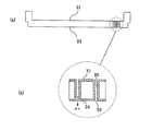
次に、本考案の第2の実施形態に係る基板処理装置について説明する。第2実施形態に係る基板処理装置は、シャワープレートの細孔23の側面に陽極酸化膜が施されていない点で、第1実施形態と異なる。
以上、本考案の特定の実施形態について説明してきたが、ここに開示される装置の構造は例示に過ぎず、実用新案登録請求の範囲に記載された本考案の思想から離れることなく、さまざまな修正及び変更が可能であることは当業者の知るところである。
Claims (5)
- リアクタと、
前記リアクタ内部に設けられた被処理体を載置するためのサセプタと、
前記リアクタの内部にあって、前記サセプタと対向して平行に配置され、ガスを前記被処理体に向けて噴射するための複数の細孔を有するシャワープレートと、
前記リアクタから離隔して設けられた遠隔プラズマチャンバと、
前記遠隔プラズマチャンバと、前記リアクタとを連結するガス導入管と、
を備え、
前記遠隔プラズマチャンバ内で、クリーニングガスが活性化され、
前記シャワープレートは、ガスが前記ガス導入管を通じて導入されるガス導入面と、前記複数の細孔を通じて前記ガスを前記被処理体の表面に噴射するガス噴射面を有し、前記ガス噴射面は膜被覆処理されているが、前記ガス導入面は膜被覆処理されていないことを特徴とする、
基板処理装置。 - 前記複数の細孔の内側面も膜被覆処理されている、ことを特徴とする請求項1記載の基板処理装置。
- 前記膜被覆処理は、陽極酸化膜処理である、ことを特徴とする請求項1または2記載の基板処理装置。
- 前記膜被覆処理は、コーティング処理である、ことを特徴とする請求項1または2記載の基板処理装置。
- 前記ガス導入面は、少なくとも化学的若しくは機械的研磨の一方の処理が施されている、ことを特徴とする請求項1から4いずれか1項記載の基板処理装置。
Priority Applications (1)
| Application Number | Priority Date | Filing Date | Title |
|---|---|---|---|
| JP2008007771U JP3147868U (ja) | 2008-11-06 | 2008-11-06 | 基板処理装置 |
Applications Claiming Priority (1)
| Application Number | Priority Date | Filing Date | Title |
|---|---|---|---|
| JP2008007771U JP3147868U (ja) | 2008-11-06 | 2008-11-06 | 基板処理装置 |
Publications (1)
| Publication Number | Publication Date |
|---|---|
| JP3147868U true JP3147868U (ja) | 2009-01-22 |
Family
ID=54781470
Family Applications (1)
| Application Number | Title | Priority Date | Filing Date |
|---|---|---|---|
| JP2008007771U Expired - Lifetime JP3147868U (ja) | 2008-11-06 | 2008-11-06 | 基板処理装置 |
Country Status (1)
| Country | Link |
|---|---|
| JP (1) | JP3147868U (ja) |
Cited By (2)
| Publication number | Priority date | Publication date | Assignee | Title |
|---|---|---|---|---|
| JP2016051864A (ja) * | 2014-09-02 | 2016-04-11 | 株式会社日立国際電気 | 半導体装置の製造方法、基板処理装置およびプログラム |
| JP2024535234A (ja) * | 2021-09-17 | 2024-09-30 | アプライド マテリアルズ インコーポレイテッド | ディフューザーの片面陽極酸化処理 |
-
2008
- 2008-11-06 JP JP2008007771U patent/JP3147868U/ja not_active Expired - Lifetime
Cited By (4)
| Publication number | Priority date | Publication date | Assignee | Title |
|---|---|---|---|---|
| JP2016051864A (ja) * | 2014-09-02 | 2016-04-11 | 株式会社日立国際電気 | 半導体装置の製造方法、基板処理装置およびプログラム |
| US9640387B2 (en) | 2014-09-02 | 2017-05-02 | Hitachi Kokusai Electric Inc. | Method of manufacturing semiconductor device, substrate processing apparatus, and recording medium |
| JP2024535234A (ja) * | 2021-09-17 | 2024-09-30 | アプライド マテリアルズ インコーポレイテッド | ディフューザーの片面陽極酸化処理 |
| JP7807533B2 (ja) | 2021-09-17 | 2026-01-27 | アプライド マテリアルズ インコーポレイテッド | ディフューザーの片面陽極酸化処理 |
Similar Documents
| Publication | Publication Date | Title |
|---|---|---|
| JP7079686B2 (ja) | 成膜方法及び成膜装置 | |
| CN109075030B (zh) | 用于在等离子体处理腔室中的原位腔室清洁效率提高的等离子体处理工艺 | |
| KR100729900B1 (ko) | 표면 처리된 샤워헤드를 구비하는 기판 처리 장치 및 기판 처리 장치의 세정 방법 | |
| KR100447284B1 (ko) | 화학기상증착 챔버의 세정 방법 | |
| KR100654121B1 (ko) | 부착막의 제거방법 | |
| JP2006128485A (ja) | 半導体処理装置 | |
| JP2001274105A (ja) | セルフクリーニング用の遠隔プラズマソースを備えた半導体処理装置 | |
| KR102007019B1 (ko) | 플라즈마 처리에 의한 불화 알루미늄 경감 | |
| US20060090773A1 (en) | Sulfur hexafluoride remote plasma source clean | |
| KR20010039780A (ko) | 발열체 cvd 장치 및 부착막의 제거방법 | |
| JP2000323467A (ja) | 遠隔プラズマ放電室を有する半導体処理装置 | |
| KR102890186B1 (ko) | 슬릿 밸브 게이트 코팅 및 슬릿 밸브 게이트들을 세정하기 위한 방법들 | |
| JP3147868U (ja) | 基板処理装置 | |
| CN100549226C (zh) | 化学气相沉积设备的清洁方法 | |
| US20070246062A1 (en) | Method of cleaning deposition chamber | |
| TWI799512B (zh) | 清洗方法及電漿處理裝置 | |
| US7972961B2 (en) | Purge step-controlled sequence of processing semiconductor wafers | |
| KR101416172B1 (ko) | 박막 증착 장비의 챔버 세정 방법 | |
| JP2003017479A (ja) | プリ・コート方法、処理方法及びプラズマ装置 | |
| TWI445082B (zh) | Plasma processing method | |
| US20250246450A1 (en) | Method for maximizing thin-films stress through season improvement | |
| JPH10189461A (ja) | プラズマ処理装置 | |
| JP2001185533A (ja) | プラズマ反応領域用構造体の製造方法およびプラズマ反応領域用構造体およびこれを用いたプラズマ処理装置 | |
| JP2001131752A (ja) | プラズマクリーニング方法 | |
| JP2001131750A (ja) | プロセスチャンバー内のクリーニング方法及び基板処理装置 |
Legal Events
| Date | Code | Title | Description |
|---|---|---|---|
| R150 | Certificate of patent or registration of utility model |
Free format text: JAPANESE INTERMEDIATE CODE: R150 |
|
| FPAY | Renewal fee payment (event date is renewal date of database) |
Free format text: PAYMENT UNTIL: 20111224 Year of fee payment: 3 |
|
| FPAY | Renewal fee payment (event date is renewal date of database) |
Free format text: PAYMENT UNTIL: 20111224 Year of fee payment: 3 |
|
| FPAY | Renewal fee payment (event date is renewal date of database) |
Free format text: PAYMENT UNTIL: 20121224 Year of fee payment: 4 |
|
| FPAY | Renewal fee payment (event date is renewal date of database) |
Free format text: PAYMENT UNTIL: 20121224 Year of fee payment: 4 |
|
| FPAY | Renewal fee payment (event date is renewal date of database) |
Free format text: PAYMENT UNTIL: 20131224 Year of fee payment: 5 |
|
| R250 | Receipt of annual fees |
Free format text: JAPANESE INTERMEDIATE CODE: R250 |
|
| R250 | Receipt of annual fees |
Free format text: JAPANESE INTERMEDIATE CODE: R250 |
|
| R250 | Receipt of annual fees |
Free format text: JAPANESE INTERMEDIATE CODE: R250 |
|
| R250 | Receipt of annual fees |
Free format text: JAPANESE INTERMEDIATE CODE: R250 |
|
| R250 | Receipt of annual fees |
Free format text: JAPANESE INTERMEDIATE CODE: R250 |
|
| EXPY | Cancellation because of completion of term |