JP3564112B2 - How to collect spacers - Google Patents
How to collect spacers Download PDFInfo
- Publication number
- JP3564112B2 JP3564112B2 JP2002098891A JP2002098891A JP3564112B2 JP 3564112 B2 JP3564112 B2 JP 3564112B2 JP 2002098891 A JP2002098891 A JP 2002098891A JP 2002098891 A JP2002098891 A JP 2002098891A JP 3564112 B2 JP3564112 B2 JP 3564112B2
- Authority
- JP
- Japan
- Prior art keywords
- spacer
- glass
- face plate
- rear plate
- plate
- Prior art date
- Legal status (The legal status is an assumption and is not a legal conclusion. Google has not performed a legal analysis and makes no representation as to the accuracy of the status listed.)
- Expired - Fee Related
Links
Images


Classifications
-
- Y—GENERAL TAGGING OF NEW TECHNOLOGICAL DEVELOPMENTS; GENERAL TAGGING OF CROSS-SECTIONAL TECHNOLOGIES SPANNING OVER SEVERAL SECTIONS OF THE IPC; TECHNICAL SUBJECTS COVERED BY FORMER USPC CROSS-REFERENCE ART COLLECTIONS [XRACs] AND DIGESTS
- Y02—TECHNOLOGIES OR APPLICATIONS FOR MITIGATION OR ADAPTATION AGAINST CLIMATE CHANGE
- Y02W—CLIMATE CHANGE MITIGATION TECHNOLOGIES RELATED TO WASTEWATER TREATMENT OR WASTE MANAGEMENT
- Y02W30/00—Technologies for solid waste management
- Y02W30/50—Reuse, recycling or recovery technologies
- Y02W30/82—Recycling of waste of electrical or electronic equipment [WEEE]
Landscapes
- Manufacture Of Electron Tubes, Discharge Lamp Vessels, Lead-In Wires, And The Like (AREA)
- Processing Of Solid Wastes (AREA)
Description
【0001】
[本発明の記載の見出し説明]
本発明の内容に関し、以下の順序で説明する。課題、解決手段、実施形態、実施例の各添え数字はそれぞれ対応して記載しています。
【0002】
(1)従来の技術
(2)発明が解決しようとする課題 課題1乃至課題13
(3)課題を解決するための手段 解決手段1乃至解決手段13
(4)発明の実施の形態 実施形態1乃至実施形態13
(5)実施例 実施例1乃至実施例13
(6)発明の効果 発明の効果1乃至発明の効果13
【0003】
【発明の属する技術分野】
本発明は、地球環境を推進するために、ガラスを主要な構成材料とする2枚の基板、即ちフェースプレート(前面ガラス基板)とリアプレート(後面ガラス基板)とが、枠を介して、フリットガラス等により気密接合されている構造を有するフラットパネルディスプレイを、廃棄のために解体処理する方法、フラットパネルディスプレイの再利用、さらにはこれに使用されている金属元素のうち、有害金属元素である鉛を分離回収し、その他の貴金属元素や希土類元素を有効再利用する方法、フリットガラスにより溶着された画像形成装置を分解し、そのフェースプレート、リアプレートを再生する方法、スペーサの回収および再利用方法、該蛍光体塗布部に電子線を照射又は紫外線を照射して発光させるフラットディスプレイ装置またはCRT(Cathode Ray Tube)からの蛍光体の回収方法及びディスプレイ装置の製造方法、分解、解体、再利用を好適とする画像表示装置、廃棄物などに含まれる有害金属量を検査する残留有害金属量の検査装置、フラットディスプレイパネルにおける蛍光体の回収方法および装置に関する。
【0004】
【従来の技術】
従来、廃棄される家電製品のほとんどはシュレッダー処理されて、金属などの有価物の回収後、残りは産業廃棄物として素掘りの穴に埋めるだけの「安定型処分場」に捨てられてきた。
【0005】
近年、処分場の容量不足の深刻化とともに、有害物質による環境汚染が問題となっている。一例をあげると、テレビのブラウン管には鉛入りガラスが多く使用されているが、環境庁の試算では廃棄されるブラウン管に含まれる鉛は毎年2万トンで、その多くが安定型処分場に埋め立てられている。しかし、安定型処分場には雨水が自然の状態で浸透し、排水施設も無いため、有害物質である鉛が拡散するおそれがあることが認識されるようになってきている。
このような状況の中で、従来の処理方法の見直しが迫られている。テレビのブラウン管については、ブラウン管ガラスをカレット(ガラス小片)化して、再びブラウン管に再利用するという実証研究が、財団法人家電製品協会によって行われている。その中で、テレビ本体からブラウン管を取り出してガラスカレットにするというシステムが開発されている(たとえば「電子技術」1997年11月号参照)。
【0006】
例えば、ガラスをカレットとして回収する方法としては、特開昭61−50688号公報などに示されている。また、ブラウン管ガラスをカレット化(ガラス小片)して、再びブラウン管に再利用する例(特開平9−193762号公報等)が、知られている。また、ブラウン管をフェースプレート部・ファンネル部と材質毎に分離し、カレット化する方法に関しては特開平05−185064号公報などに示されている。更にブラウン管をフェースプレート部とファンネル部とに分離し、蛍光体及びブラックマスクをフェースプレート部から剥離した後、フェースプレートを再生する方法としては特開平7−037509号公報に示されている。
【0007】
ブラウン管ガラスの再利用のためには、パネルガラスと鉛入りのファンネルガラスに区分けして処理する必要がある。これは、パネルガラスに鉛が所定量以上混入すると、ブラウニング現象が生じるため、鉛の混入したガラスはパネルガラスの原料としては再利用できなくなるためである。そのためにまず、パネル部とファンネル部に分離する工程があるが、これには、位置を規定して切断する方法(特開平9−115449号公報)や、パネル部とファンネル部を接合するフリットガラスを溶解して分離する方法(特開平7−45198号公報)が提案されている。
【0008】
フリットガラスで融着されたファンネル部とパネル部を分離する技術としては、例えば特開平5−151898号公報,特開平7−029496号公報,特開平9−200654号公報,特開平9−200657号公報などの公報に開示された熱処理時の熱歪みを利用してファンネル部とパネル部を分離するような技術が知られている。
【0009】
一方、近年、冷陰極素子を応用するための研究が盛んに行われてきている。冷陰極素子としては、表面伝導型放出素子や、電界放出型素子や、金属/絶縁層/金属型放出素子などが知られており、熱陰極素子と比較して低温で電子放出を得ることができるため、加熱用ヒーターを必要とせず、熱陰極素子よりも構造が単純であり、微細な素子を作成可能である。また、基板上に多数の素子を高い密度で配置しても、基板の熱溶融などの問題が発生しにくい。また、熱陰極素子がヒーターの加熱により動作するため応答速度が遅いのとは異なり、冷陰極素子の場合には応答速度が速いという各利点もある。
【0010】
冷陰極素子のなかでも特に表面伝導型放出素子は、構造が単純で製造も容易であることから、大面積にわたり多数の素子を形成できる利点がある。そこで、たとえば本出願人による特開昭64−31332号公報において開示されるように、多数の素子を配列して駆動するための方法が研究されている。
【0011】
また、表面伝導型放出素子の応用については、たとえば、画像表示装置、画像記録装置などの画像形成装置や、荷電ビーム源等が研究されている。
【0012】
特に、画像表示装置への応用としては、たとえば米国特許第5,066,883号明細書、特開平2−257551号公報、あるいは特開平4−28137号公報において開示されているように、表面伝導型放出素子と電子ビームの照射により発光する蛍光体とを組み合わせて用いた画像表示装置が研究されている。表面伝導型放出素子と蛍光体とを組み合わせて用いた画像表示装置は、従来の他の方式の画像表示装置よりも優れた特性が期待されている。たとえば、近年普及してきた液晶表示装置と比較しても、自発光型であるためバックライトを必要としない点や、視野角が広い点が優れていると言える。
【0013】
また、電界放出型素子を多数個ならべて駆動する方法は、たとえば米国特許4,904,895号の明細書に開示されている。また、FE型を画像表示装置に応用した例として、たとえば、R.Meyerらにより報告されたフラットディスプレイが知られている[R.Meyer:”Recent Development on Micro−tips Displayat LETI”, Tech. Digest of 4th Int. Vacuum Micro−electronics Conf., Nagahama,pp.6−9 (1991)]。
【0014】
また、金属/絶縁層/金属型放出素子を多数個並べて画像表示装置に応用した例は、たとえば特開平3−55738号公報に開示されている。
【0015】
上記のような電子放出素子を用いた画像形成装置のうちで、奥行きの薄いフラットディスプレイは省スペースかつ軽量であることから、ブラウン管型の表示装置に置き換わるものとして注目されている。
また、上記画像形成装置中の気密容器の内部は、10のマイナス6乗Torr程度の真空に保持されており、画像表示装置の表示面積が大きくなるにしたがい、気密容器内部と外部の気圧差によるリアプレートおよびフェースプレートの変形あるいは破壊を防止する手段が必要となる。リアプレートおよびフェースプレートを厚くすることによる方法は、画像表示装置の重量を増加させるのみならず、斜め方向から見たときに画像のゆがみや視差を生ずる。これに対し、比較的薄いガラス板からなり、表面に帯電防止のための導電膜を形成したスペーサが設けられる場合が一般的である。
以上説明した電界放射型電子源ディスプレイ(FED)、MIM型ディスプレイに加えて、蛍光表示ディスプレイ(VFD)、プラズマディスプレイ(PDP)、表面伝導型電子源ディスプレイ(SED)などを含む、フラットディスプレイは省スペースかつ軽量であることから、ブラウン管型の表示装置に置き換わるものとして注目されており、多くの研究開発が行われてきた。
【0016】
例えば、本出願人は冷陰極型の電子放出素子の一種である表面伝導型電子放出素子を基体上に多数配置した電子源と、これを用いた画像表示装置に関していくつかの提案を行っている。
【0017】
この表面伝導型電子放出素子の構成やこれを用いた画像表示装置の構成などに関しては、例えば特開平7−235255号公報に詳しく述べられているので、簡単に説明する。
【0018】
図68(a)(b)に表面伝導型電子放出素子の構成の一例を示す。411は基体、412,413は一対の素子電極、414は導電性膜で、その一部に電子放出部415を有し、電子放出素子416を構成する。
【0019】
電子放出部415を形成する方法としては、上記一対の素子電極412,413の間に電圧を印加して、上記導電性膜の一部を変形、変質ないし破壊して高抵抗することにより行う方法があり、これを「通電フォーミング処理」と称する。この方法により電子放出特性の良い電子放出部を形成するためには、上記導電性膜は導電性微粒子により構成されたものであることが好ましい。その材質としては、例えばPdO微粒子が挙げられる。通電フォーミング処理において印加される電圧は、パルス電圧が好ましく、図69(a)に示すような波高値が一定のパルスを印加する方法、あるいは図69(b)に示すような、波高値が漸増するパルスを印加する方法のいずれも適用できる。
【0020】
導電性微粒子膜を形成するには、ガスデポジション法により直接、導電性微粒子を堆積させることも可能であるが、導電性膜の構成元素を含む化合物(例えば有機金属化合物)の溶液を塗布し、これを熱処理などによって所望の導電性膜とする方法が、真空装置を必要とせず、製造コストが安く、大型の電子源を形成するのに適用しやすい、等の理由から望ましい方法である。また、上記有機金属化合物の溶液を塗布する方法としてはインクジェット装置を用いて必要な部分のみに塗布する方法が、導電性膜のパターニングのための余分な工程を必要としないため、一層望ましいものである。
【0021】
電子放出部を形成した後、有機物質を含む適当な雰囲気中で、素子電極間にパルス電圧を印加することにより(これを「活性化処理」と呼ぶ)、電子放出部とその近傍に炭素を主成分とする堆積膜が形成され、素子に流れる電流が増大し、電子放出特性も向上する。
【0022】
次いで、好ましくは「安定化処理」と呼ばれる工程を行う。これは、真空容器や電子放出素子を加熱しながら排気を続けることにより、有機物質などを十分に除去し、電子放出素子の特性を安定化させる処理である。
【0023】
このような、表面伝導型電子放出素子を用いた電子源の導電性膜を、インクジェット装置を用いて形成する方法に関しては、特開平8−273529号公報などに開示されている。
【0024】
インクジェット装置について簡単に説明する。インクジェット装置の、インクを吐出する方式には大きく分けて2つの種類がある。第1の方法は、ノズルに配設されたピエゾ素子の収縮圧力により液体の液滴を吐出する方法で、ピエゾジェット方式と呼ぶ。この方式は、導電体薄膜材料をインク溜に貯め、電気信号入力端子に所定の電圧を印加することにより、上記円筒形ピエゾが収縮し、液体を液滴として吐出させるものである。
【0025】
第2の方法は発熱抵抗体により液体を加熱発泡させ、これにより液滴を吐出する方法で、バブルジェット(登録商標)方式と呼ぶ。バブルジェット(登録商標)方式によるインクジェット装置は、発熱抵抗体が発熱して、液体が発泡し、これによりノズルから液滴が吐出される。
【0026】
上述のようなインクジェット装置を用い、所定の位置にのみ有機金属化合物の溶液を液滴として付与し乾燥させた後、加熱処理により該有機金属化合物を熱分解することにより、金属あるいは金属酸化物などの微粒子からなる導電性膜が形成される。
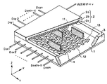
図1に画像表示装置の構成の一例を示す。図1において、1はリアプレート、2は基板2aの内面に蛍光膜2bとメタルバック2c等が形成されたフェースプレート、3は支持枠であり、リアプレート1、支持枠3およびフェースプレート2をフリットガラスで封着・密封して画像表示装置15を構成する。
【0027】
以上に記したような構成のフラットパネルディスプレイは、今後、その大型化と生産量の飛躍的増大が予想されている。また、これらのフラットパネルディスプレイについては封着に用いるフリットガラスに鉛が含まれており、また、画像形成部材をなす蛍光体2b、及びスペーサ4等は高コスト部材になっていることから、ブラウン管ガラスの場合と同様に、「無害化」,「減容化」,「再資源化」の面から回収システムの確立が重大な課題となっている。
【0028】
【発明が解決しようとする課題】
以下、本発明が解決しようとする課題をそれぞれ以下の順番で記載して、その順序に従って、解決手段及び実施形態更に実施例について説明する。
【0029】
[課題1]FPDは、ブラウン管とは構造が異なるため、別の処理方法が必要である。すなわちFPDは、ガラスを主要な構成材料とする2枚の基板、即ちフェースプレートとリアプレートとが、枠を介してフリットガラスにより気密接合されている構造を有する。フリットガラスは、一般に低温焼成が可能なように、鉛成分の多いものが使用されている。
【0030】
ブラウン管と同様の理由で、ガラスの再利用のためには、鉛を含まないガラスと鉛入りのガラスとに区分けして処理する必要がある。さらにガラス以外の部材を再利用するにあたっても、鉛を除去する工程が必要である。
【0031】
本発明は、上記課題を解決するためになされたものであり、その目的は、廃棄されるFPDの再利用を容易にするための処理方法を提供することである。
【0032】
[課題2]また、本発明の課題は、有害金属である鉛の分離回収方法や、貴金属元素や希土類元素等の希少元素の回収再利用方法も含めた解体処理方法を提供することである。
【0033】
[課題3]また、フラットディスプレイが製造過程での不良発生、あるいは耐用年数の経過などにより廃棄される場合、ディスプレイ全体をシュレッダー処理して廃棄すると廃棄量が多くなる。近年、産業活動に伴う廃棄物の発生を極力制御することが社会的に要請されており、部材の再利用は、緊急性の高い課題となっている。
【0034】
また、構成材料に有害元素等が含まれていた場合、分離して処理する必要がある。さらに、画像表示装置の性能を左右する電子放出素子を有するリアプレートは、均一な素子特性を得るために高価な基板を用いることが多い。中でも、リアプレート用基板の最初に形成する素子電極は、あとの工程でも耐えられる強固な材料を用いることが多い。
【0035】
本発明は、上記課題を解決するためになされたものであり、その目的は廃棄される画像表示装置の重要な構成部品であるリアプレートの再利用をし易くするための解体方法を提供することである。さらに、構成材料に含まれる鉛等の元素の分離回収方法を提供することである。さらに、リアプレート再生時に、複数構成される電子放出素子の電子放出部を含む導電性膜を最小限の原料で効率よく形成することである。
【0036】
[課題4]また、フラットディスプレイが製造過程での不良発生、あるいは耐用年数の経過などにより廃棄される場合、ディスプレイ全体をシュレッダー処理して廃棄するのは、構成材料に比較的高価な部材が含まれていることから経済的にも好ましくない。特に上述のスペーサは、パネル中に多数用いられている上に、その製造にはガラスの薄片化や導電膜の形成などを必要とする、非常に製造コストおよび時間がかかる部品である。また、ディスプレイが何らかの理由で廃棄される場合でも、その原因がスペーサの不良であることはごく希であり、再利用に支障がないことが多い。
【0037】
このような理由から、フラットディスプレイを廃棄する際に、スペーサを他の部材から分離して回収し、再利用することが望まれている。
【0038】
しかし今述べたように、スペーサは薄い板状であり、かつガラスを基板としているため、ディスプレイの分解途中で損傷を受けることが懸念されることから、損傷を受けないように回収することができる方法の開発が望まれている。
【0039】
[課題5]また、従来、使用後廃棄されたディスプレイ装置からの希土類元素の回収は殆ど行われてこなかった。
【0040】
この原因としては、(1).希土類元素のディスプレイ装置一台当たりの使用量が少なく回収が困難である、(2).希土類元素が単体ではなく化合物または合金の形で使用されているので単離にコストがかかる、(3).比較的安価な輸入希土類元素が、円高の影響でより安価に入手可能である、ことなどが挙げられる。
【0041】
しかしながら、環境保全及び希少元素資源の安定供給の面から、これらの材料のリサイクルの推進を行なっていくことが望まれ、工業製品からの希土類元素の回収方法は重要課題となる。尚、希土類元素は主に蛍光体中に含有されている。
【0042】
また、蛍光体中にはクロム及び硫黄元素も含有されており、環境保全の面からはこれらの回収も望まれている。
【0043】
一方、従来の方法で蛍光体を回収した後のフェースプレートは、その内面の平滑性がほとんど失われる。そのため、従来はカレット化して、安定型処分場に埋め立てる、ガラス素材として再利用に供するといった方法が採られてきた。更にカレット化を行なわずに、内面の平滑性を酸処理などによって再生しフェースプレートとして再利用するなどの方法も近年考案されてきている。しかし、安定型処分場はもはや飽和状態となってきており有効な方法ではなくなってきている。また酸処理は湿式処理であるためコスト及び作業環境上好ましくない。
【0044】
本発明は、上述した事情に鑑みなされたものであり、ディスプレイ装置に含有される蛍光体を効率的に回収し、なお且つ内面の平滑性を保持したままで、または再生してフェースプレートを回収し、再利用する方法を提供するものである。
【0045】
[課題6]また、大気圧に対する低圧力に保たれた気密容器を有する画像表示装置を、分解、解体して再利用しようとするには、気密容器内を大気圧に戻す必要がある。大気圧にする際、該気密容器内部との圧力差が大きいほど、気密容器内部に急激に空気等のガスが流入し、気密容器内部を傷つけたり、気密容器を破壊することが多い。また、予期せぬ破壊が起こり、破片がまわりに飛び散る等安全上も好ましくない。加えて、CRTをカレット化し、ガラス材料として再利用する場合は、大きな問題にならなかったが、画像表示装置の各部材を最大限再利用することを考えると、これらの破壊は、資源保護の観点からみて、ごみ等の廃棄物を増やすだけでなく、エネルギー、労働力の浪費につながる。特に、FPDでは、容器内部にスペーサ等の耐大気圧構成部材を多く設けているため、これらの破損が激しく、耐大気圧構成部材が破損するだけでなく、破損した部材が画像表示装置の気密容器内部を傷つけ破損させ、これら部材の再利用を著しく妨げていた。また、スペーサは画像の乱れを防ぐため、側面形状を均一にしたり、画像表示装置の仕様に応じた導電率を持つ膜を均一にコートしたりと、他の部材に比べても大きなコストを占めている部材である。
【0046】
本発明は、上記課題を解決するためになされたものであり、その目的は、画像表示装置を真空排気された気密内をスムーズに外部圧に戻すことにより、分解、解体する際、部材の再利用を可能にするものである。
【0047】
[課題7]また、フラットディスプレイが製造過程での不良発生、あるいは耐用年数の経過などにより廃棄される場合、ディスプレイ全体をシュレッダー処理して廃棄するのは環境上問題であり、かつ素子の構成材料に比較的高価な部材が含まれていることから経済的にも好ましくない。例えばスペーサはパネル中に多数用いられている上に、その製造にはガラスの薄片化や導電膜の形成などを必要とし、製造コスト及び時間を要する。またリアプレートやフェースプレート、支持枠においては、その状況に応じてリペアが必要な箇所に適当な処理をした上で再利用することも可能である。
【0048】
このような理由から、製造過程での不良発生および耐用年数の経過などによりフラットディスプレイを解体する際に、損傷なく部材を回収して再利用化を図ることや効率よく資源を回収することが望まれている。
【0049】
そこで本発明の目的は、フラットディスプレイを安全かつ簡易的な方法で各構成部材に分解する方法を提供すること及びこのような解体に適した構成を有するフラットディスプレイパネルを提供することにある。
【0050】
[課題8]また、ブラウン管やフラットパネルディスプレイなどの解体,分別処理においては、前述した環境汚染,破壊の問題から、再利用のための分別部材を回収した残りの廃棄物について有害金属量を定量的に検出して、その残留量が許容値以下であることを検査,確認する必要がある。そして、再利用のための分別部材についても、前述したブラウン管ガラスのように、鉛の有無により分別する必要性から、鉛(有害金属)の残留量を定量的に知りたいという要求がある。
【0051】
ここに、部材中の鉛を検出するには、例えば蛍光X線等により検査する方法が知られているが、それでは検査対象の部材全面を走査する必要があるため、カレット化したガラスなど検査対象が多数になると手間がかかり、検査し得る対象が限定され、そして定量的な検出は行えなく適用が難しい。
【0052】
そこで、本発明はそうした従来の課題に鑑みてなされたものであって、フラットパネルディスプレイなどの解体,分別処理に際して、ガラスからなる分別部材及び廃棄物等の検査対象に残留した鉛等の有害金属量を定量的に検出することができ、検査対象は特に制限なく各種の部材を検査でき、その定量検出を手間なく容易に行うことができる残留有害金属量の検査装置を提供することを目的とする。
【0053】
[課題9]また、フラットパネルディスプレイについて、リサイクルするための解体処理の技術はまだ開発途上にあり、従来公知の関連技術をそのまま流用することはできない。例えば前述した特開平9−193762号公報などに開示されたブラウン管ガラスの解体処理の技術を用いると、スペーサ4を分離させる際に、リアプレートまたはフェースプレートの重量が荷重されてしまい、このためスペーサを破損してしまうという問題があり、フラットパネルディスプレイの解体には適用できない。
【0054】
そこで、本発明はかかる従来の課題に鑑みてなされたものであって、解体処理を適切な工程により行えて、そのまま再利用し得るスペーサ等の構成部材を破損することなく回収でき、再資源化を好ましく図れるフラットパネルディスプレイの解体装置を提供することを目的とする。
【0055】
[課題10]また、FPDはブラウン管とは構造が異なるため、別の処理方法が必要である。上記のFPDはガラスを主要な構成材料とする2枚の基板、即ちフェースプレートとリアプレートとが、枠を介して、フリットガラスにより気密接合されている構造を有する。フリットガラスは一般に低温焼成が可能なように鉛成分の多いものが使用されている。また、フリットガラスの他にも、配線材料や、フェースプレートの構成材料に鉛が含まれている場合がある。FPDの場合も、ブラウン管と同様の理由で、ガラスの再利用のためには、鉛を含まないガラスと鉛入りのガラスに区分けして処理する必要がある。さらにガラス以外の部材を再利用するにあたっても、鉛を除去する工程が必要である。
【0056】
鉛を除去するためには、酸やアルカリの水溶液を用いて鉛成分を選択的に溶解させて分離する方法が有効である。この方法を大規模に実施するためには、鉛を溶解させるための大量の水溶液と、その後の洗浄工程のための大量の水が必要である。また液体を加熱したり流動させたりするために、多くのエネルギーを投入しなければならない。その結果、処理コストが増大するという課題があった。
【0057】
本発明は上記課題を解決するためになされたものであり、その目的は廃棄されるFPDを少ないコストで処理する方法を提供することである。
【0058】
[課題11]また、用後廃棄されたディスプレイからの希土類元素の回収は殆ど行われてこなかった。この原因として、(1).希土類元素のディスプレイ1台当たりの使用量が少なく、その回収が困難であり自動化も進んでいない。(2).希土類元素が単体ではなく、化合物または合金の形で使用されているので単離にコストがかかる。(3).比較的安価な輸入希土類元素が、円高の影響でより安価に入手可能である。などの点が挙げられる。
【0059】
しかしながら、環境保全および希少元素資源の安定供給の面から、これらの材料のリサイクルの推進を行なっていく必要があり、工業製品からの希土類元素の回収方法は重要課題となってきている。CRTに関しては回収事業を開始した家電メーカがある一方で、フラットパネルディスプレイにおいても早急にリサイクルの推進を図る要請が高まっている。
【0060】
本発明はかかる実情に鑑み、フラットパネルディスプレイにおいて効率的かつ簡便に分解し、有効に特に蛍光体を回収し得る蛍光体の回収方法および装置を提供することを目的とする。
【0061】
[課題12]また、FPD(フラットパネルディスプレイ)はブラウン管とは構造が異なるため、別の処理方法が必要である。つまりFPDはガラスを主要な構成材料とする2枚の基板、すなわちフェースプレート2とリアプレート1とが枠を介して、フリットガラスにより気密接合されている構造を有する。フリットガラスは一般に低温焼成が可能なように鉛成分の多いものが使用されている。また、フリットガラスの他にも、配線材料やフェースプレートの構成材料に鉛が含まれている場合がある。FPDの場合もブラウン管と同様の理由で、ガラスの再利用のためには、鉛を含まないガラスと鉛入りのガラスに区分けして処理する必要がある。さらにガラス以外の部材を再利用するにあたっても、鉛を除去する工程が必要である。
【0062】
鉛を除去するためには、酸やアルカリの水溶液を用いて鉛成分を選択的に溶解させて分離する方法(液体中処理)が有効である。この方法を大規模に実施するためには、鉛を溶解させるための大量の水溶液と、その後の洗浄工程のための大量の水が必要である。また液体を加熱したり流動させたりするために、多くのエネルギを投入しなければならない。そのためコストを抑制して短時間で処理を行うためには、廃棄FPDを解体して得られるガラス板を多数まとめて、液体中処理槽へ投入し、処理する必要がある、また、処理槽間を迅速に搬送するためには多数のガラス板を一括して送る搬送機構が必要となる。
【0063】
本発明はかかる実情に鑑み、効率的かつ的確な液体中処理を実現する基板処理方法および装置を提供することを目的とする。
【0064】
[課題13]また、基板ガラスを再利用するに際して、リアプレート1およびフェースプレート2を他の部材と分離する。そして基板上に形成された配線や素子等を除去してガラス単体の状態に戻した上で、そのまま基板として再使用し、あるいは一度カレット化した後新たに基板用のガラスあるいは他製品の原料として再利用することが可能である。
【0065】
ところが上記のようにガラス基板上には配線や電子放出素子、フリットガラス等の材料が構成されている上に、前述のように青板ガラスを基板として使用する場合には、あらかじめ表面に薄膜を形成している場合もある。このような材料の中にはガラス基板との密着性が極めて高いものや、あるいは一部の元素においては徐々にガラス基板中に拡散することが起こり得るため、基板ガラスとの完全な分離が困難なことがある。
【0066】
また、使用済みのガラスを一度カレット化した後に再利用する場合、カレット化したガラス中にガラス構成元素以外の元素が混入してしまうと、ガラスの物性および色に影響を及ぼす。したがって不純物元素の混入したガラスは再利用できないことがある。またそのまま基板として再使用するに場合でも、可能な限り初期のガラス基板に近い状態に戻すことが望まれる。
【0067】
本発明はかかる実情に鑑み、基板ガラスの有効かつ効率的な再利用を実現するガラス基板の処理方法を提供することを目的とする。
【0068】
【課題を解決するための手段】
本発明の課題を解決する手段として、上述の各発明が解決しようとする課題に対応した順序に従って、説明する。
【0069】
[解決手段1] 上記目的を達成するために本発明は、ガラスを主要な構成材料とする2枚の基板、即ちフェースプレートとリアプレートとが、枠を介して、フリットガラスにより気密接合されている構造を有するFPDの解体処理方法において、フリットガラスにより接合された枠の部分をその他の部分から分離することを特徴とする。
【0070】
さらに本発明は、内部にスペーサを有し、フェースプレート内面に蛍光面を有する、FPDの解体処理方法において、フリットガラスにより接合された枠の部分を分離する際、残りの部分にスペーサおよび、蛍光面が残るようにすることを特徴とする。
【0071】
さらに本発明は、フェースプレートとリアプレートの一部を切断することにより、フリットガラスにより接合された枠の部分をその他の部分から分離することを特徴とする。
【0072】
本発明において、切断位置を決定する手段は、フリットガラスにより接合された枠の部分の位置の検知を行う手段(ビデオカメラ)によって構成される。
【0073】
[解決手段2] 上記目的を達成するため本発明は、ガラスを主要な構成材料とする2枚の基板、即ち、フェースプレートとリアプレートとが、枠を介して、フリットガラスにより気密接合されている構造を有するFPDにおいて、その接合部を硝酸溶解させて剥離することを特徴とする。更に、本発明は、内部にフリットガラスにより接合されているスペーサを有する場合もある。
フリットガラスを硝酸に溶解する方法としては、硝酸をフリット接合部の奥深く浸透させる必要があるため、硝酸に浸漬する方法が安全かつ容易である。本発明ではこの方法を用いているが、他に接合部に硝酸をノズル吹き付けする方法等があり、この限りではない。
硝酸に溶解させるフリット接合部は、(1)全ての接合部分を硝酸に浸漬して溶解剥離し、各部を分離して廃棄、再利用する方法と、(2)再利用したい部分を酸で侵食せずに残して、その他の部分を硝酸に浸漬して溶解剥離し廃棄する方法とに大別できる。いずれの方法においても、硝酸に溶解する金属成分のうち、有害な鉛成分のみ分離しその他の元素は回収再利用することができる。
【0074】
[解決手段3] 上記目的を達成するため本発明のリアプレート再生方法は、一対の素子電極と導電性膜からなる電子放出素子が複数設けられたリアプレート、前記電子放出素子から放出された電子が衝突することにより画像が形成される画像形成部材が設けられたフェースプレート、前記リアプレートとフェースプレートをつなぎ、内部圧力を維持する支持枠から少なくともなり、これらがフリットガラスで溶着された画像表示装置を廃棄する際に、溶着部を硝酸溶液中に浸漬してフリットガラスを溶解する工程、導電性膜をインクジェット方式で形成する工程を含んだリアプレートを回収再利用する方法である。
【0075】
本発明によれば機械的な切断等によらず、フリットガラスを化学的に溶解してリアプレートを分解するため、リアプレート基板や素子電極に、ほとんど損傷を与えることなく回収、再利用することが可能なことから、廃棄物の減少と資源の有効活用ができ、コストの削減を実現できる。さらに、Pb等の元素は、浸漬した硝酸溶液中に溶け出すので容易に回収することができる。さらに、リアプレートの再生時に、導電性膜をインクジェット方式で形成することで、必要部分にのみ導電性膜形成用材料を用いるため導電性膜材料は、最小限の量で良い。また、導電性膜形成後に不良が発見された場合でも、不良部分のみ再形成することも可能である。
【0076】
[解決手段4] 本発明は、上記の要望に鑑みてなされたものである。すなわち本発明は、複数の電子放出素子が配置されたリアプレートと、該リアプレートに対向して配置され画像表示部が設けられたフェースプレートと、枠部と、該リアプレートと該フェースプレートとの間隔を大気圧に対して保持するためのスペーサとを少なくとも有し、かつこれらがフリットガラスにより溶着されたフラットディスプレイにおけるスペーサの回収方法であって、前記スペーサとリアプレートあるいはフェースプレートとの溶着部を硝酸溶液中に浸漬してフリットガラスを溶解する際に、スペーサ同士あるいはスペーサと周辺部材との接触を回避するためのスペーサ回収治具を用いることを特徴とするスペーサの回収方法を提供するものである。
【0077】
本発明の一態様において使用されるスペーサ回収治具は、スペーサが収納できる程度の大きさの凹部を1つまたは複数有する平面板である。また別の態様におけるスペーサ回収治具は、個々のスペーサを挟み保持することが可能な先端部と、その先端部を任意の方向に動かすことができるアーム部を有する。
【0078】
本発明によれば、フラットディスプレイを分解する過程において、スペーサにほとんど損傷を与えることなく回収することが可能なことから、再利用が容易であり、資源を有効に利用することができ、コストの削減を実現できる。また回収工程においては細かな手作業を必要としないため、安全に回収することが可能である。
【0079】
[解決手段5] 本発明のディスプレイ装置からの蛍光体の回収方法は、基体に蛍光体が塗布され、該蛍光体を発光させることで表示を行うディスプレイ装置からの蛍光体の回収方法であって、前記基体に塗布された蛍光体の回収がブラシと吸引器との併用によって行われることを特徴とする。
【0080】
本発明のディスプレイ装置の製造方法は、上記本発明のディスプレイ装置からの蛍光体の回収方法を用いて蛍光体が除去された基体を、ディスプレイ装置に再利用することを特徴とする。
【0081】
本発明は、CRT、フラットディスプレイ装置といった、フェースプレート等の基体に蛍光体が塗布され、電子線の照射や紫外線により蛍光体を発光させる形態のディスプレイ装置からの蛍光体及びフェースプレート等の基体の回収に有効で、蛍光体が塗布された基体面をブラシで掃引し、蛍光体、または蛍光体とブラックマトリックス成分を掃出しつつ、基体面の平滑性を保持または損傷がある場合には再生し、掃引とともに吸引器で蛍光体、ブラックマトリックス成分を吸引して為され、蛍光体やブラックマトリックスは更に蛍光体分離プロセスに回され、フェースプレート等の基体は表面の平滑性を保持または損なわない形で工程より搬出され、そのままフェースプレート等の基体として再利用される。
【0082】
なお、蛍光体を発光させることで表示を行うフラットディスプレイ装置としては、電子線を照射する方式のものとして、後述する電子放出素子を用いたディスプレイ装置や低速電子線により発光させる蛍光表示管があり、紫外線を用いる方式のものとして、プラズマディスプレイ装置が挙げられる。蛍光体は、背面から電子線や紫外線が照射され、表面から可視光が放出される場合はフラットディスプレイ装置のフェースプレート側に塗布されるが、例えば蛍光表示管のように、低速電子線が蛍光体に照射される面から可視光が放出される場合はリアプレート側に蛍光体が塗布される。
【0083】
[解決手段6] 本発明による画像表示装置は、上記目的を達成するため、画像を表示する表示手段と、気密容器と、必要に応じて前記気密容器内を徐々に前記気密容器外の圧力に近づける手段とを備えることを特徴とする。
【0084】
また、本発明は、上記画像表示装置において、更に排気装置を備え、前記気密容器外の圧力に近づける手段は、前記排気装置に接続する手段とは上記気密容器の異なる位置にあることを特徴とする。また、前記気密容器外の圧力に近づける手段は、必要に応じたフィルターを設けたことを特徴とする。
【0085】
また、本発明は、画像を表示する表示手段と、外部圧力を維持する気密容器と、気密容器内の耐大気圧構造部材と、前記気密容器内を排気する排気装置に接続する手段と、必要に応じて前記気密容器内を徐々に前記気密容器外の力に近づける手段とを備えることを特徴とする。
【0086】
上記構成の画像表示装置では、気密容器内を徐々に大気圧に戻す手段を有するため、分解、解体時に、気密容器内の部材に圧力変化によるストレスがかかりにくい。
【0087】
従って、部材が壊れにくく、壊れた部材の破片による2次的ダメージをも、防ぐことを可能にする。
【0088】
[解決手段7] 本発明は、複数の電子放出素子が配置されたリアプレートと、該リアプレートに対向して配置され画像表示部が設けられたフェースプレートと、支持枠と、該リアプレートと該フェースプレートとの間隔を大気圧に対して保持するためのスペーサとを少なくとも有し、かつこれらがフリットガラスにより溶着されたフラットディスプレイにおいて、リアプレートと支持枠の接合とフェースプレートと支持枠の接合に軟化温度の異なるフリットガラスが用いられており、かつスペーサと基板との接合には前記2種類のうち、より軟化温度の高いフリットガラスと同じあるいはそれ以上の軟化温度を有するフリットガラスが用いられていることを特徴とする。
【0089】
ここで、上記複数のフリットガラスはいずれも、他のフリットガラスに対し軟化温度が20℃以上異なることを特徴とする。
【0090】
また本発明におけるスペーサは、リアプレートまたはフェースプレートのどちらか一方の基板に接合されていることを特徴としている。
【0091】
本発明のフラットディスプレイの解体方法は、パネルを最も軟化温度の低いフリットガラスの軟化温度以上及び他のフリットガラスの軟化温度以下に加熱し、最も軟化温度の低いフリットガラスのみを溶解して該フリットガラスで接合された接合部のみを選択的に分離し、さらに同様の手順を繰り返すことにより、軟化温度の低いフリットガラスを用いた接合部から順次分離することを特徴とする。
【0092】
ここで、最も軟化温度の高いフリットガラスによって接合された接合部を分離する方法としては、該フリットガラスを軟化温度以上に加熱して溶融、分離する方法を用いてもよく、また該フリットガラスを適当な溶媒により溶解して、分離する方法を用いてもよい。
【0093】
また、複数の電子放出素子が配置された基板と、該基板に対向して配置され画像表示部が設けられた基板とを、少なくとも格納した気密容器を有するフラットディスプレイにおいて、前記各基板及び気密容器の接合箇所が、解体時の順番に応じた異なる軟化温度のフリットガラスにより接合されていることを特徴とするフラットディスプレイでも良い。
【0094】
また、複数の電子放出素子が配置されたリアプレートと、該リアプレートに対向して配置され画像表示部が設けられたフェースプレートと、該基板間を支持する支持枠と、を少なくとも構成部材として有し、かつこれらの構成部材がフリットガラスにより溶着されたフラットディスプレイにおいて、前記リアプレートと前記支持枠との接合と、前記フェースプレートと前記支持枠との接合に軟化温度の異なるフリットガラスを用いて溶着したことを特徴とするフラットディスプレイでも良い。
【0095】
また、電子放出素子を格納した外囲器を有するフラットディスプレイにおいて、該外囲器を構成するリアプレートと支持枠の接合部、フェースプレートと支持枠の接合部に軟化温度の異なる2種類のフリットガラスを用い、かつ前記基板間を支持するスペーサと少なくとも一方の前記基板との接合部には、前記2種類のフリットガラスの軟化温度より高いかあるいはどちらか一方と同じ軟化温度のフリットガラスを用いて接合されていることを特徴とするフラットディスプレイでも良い。
【0096】
また、前記フラットディスプレイの解体に際し、該フラットディスプレイを段階的に加熱し、前記軟化温度の低いフリットガラスを用いた接合部から順次融解、分離しながら解体していくことを特徴とするフラットディスプレイの解体方法でもある。
【0097】
本発明のフラットディスプレイにおいては、外囲器を形成する部材を順次分離できることから、解体過程において外囲器及び内部の部材に損傷を与えることなく安全かつ簡易的な方法で部材を回収できる。従って再利用可能な状態で回収することが容易となり、資源の有効利用やコストの削減が実現できる。
【0098】
[解決手段8] 上記した目的を達成するために本発明の請求項1に示す残留有害金属量の検査装置は、リサイクルするため解体して分別した部材及び廃棄物などの検査対象に含まれる鉛等の有害金属量を検査する残留有害金属量の検査装置であって、前記検査対象を浸す浴槽に、当該検査対象に含まれる有害金属を溶出させる酸性液を有する第一溶出手段と、前記第一溶出手段により溶出させた後の前記検査対象を洗浄する洗浄手段と、前記洗浄手段により洗浄した後の前記検査対象を浸す浴槽に、当該検査対象に残留している有害金属を溶出させる酸性液を有する第二溶出手段と、前記第二溶出手段の酸性液中に溶出された有害金属量を定量的に検出する定量検出手段とを備えて構成する。
【0099】
上述の残留有害金属量の検査装置は、まず第一溶出手段の浴槽に検査対象を浸すと、浴槽の酸性液により当該検査対象に含まれる有害金属が溶出させられる。次に、その検査対象を洗浄手段に送って洗浄し、この後、第二溶出手段の浴槽に浸すと、浴槽の酸性液により当該検査対象に残留している有害金属が溶出させられる。そして、この溶出液を定量検出手段に送り込めば、その定量検出手段が溶出液中に含まれている有害金属量を定量的に検出する。
【0100】
従って、フラットパネルディスプレイなどの解体,分別処理に際して、ガラスからなる分別部材及び廃棄物等の検査対象に残留した鉛等の有害金属量を定量的に検出することができる。
【0101】
[解決手段9] 本発明のフラットパネルディスプレイの解体装置は、リアプレートとフェースプレートとの間に枠部材を配置して平面型の真空容器とし、両プレート間の隙間を大気圧に耐えて保持するスペーサを、それら両プレートあるいは何れか一方のプレートに固着させたフラットパネルディスプレイについてリサイクルする解体を行うものであって、前記真空容器から前記枠部材を分離させる工程を行うため前記スペーサと固着状態にある側のプレートに引上力を加えて支持する第一支持手段と、前記枠部材を分離した後に前記スペーサと固着状態にある側のプレート縁部を受け支持する第二支持手段と、前記第二支持手段により受け支持されたプレートからスペーサを分離させる工程を行うスペーサ回収手段とを備えて構成する。
【0102】
また、本発明のフラットパネルディスプレイの解体装置は、前記真空容器から前記枠部材を分離させる工程を行った後に前記第一支持手段から支持物の前記プレートを受け取って当該プレートの縁部を受け支持して、これを前記第二搬送手段に搬送する搬送手段を備えて構成する。
【0103】
さらに、本発明のフラットパネルディスプレイの解体装置は、前記搬送手段を、前記スペーサと固着状態にある側のプレートの荷重を該スペーサにかけない構造をもって構成する。
【0104】
以上の構成により本発明のフラットパネルディスプレイの解体装置は、真空容器から枠部材を分離させる工程に際して、スペーサと固着状態にある側のプレートを、第一支持手段により引上力を加えて支持するので、スペーサは吊り下げ状態になり、これと固着しているプレートの重量が加わらなく、枠部材の分離をスペーサに負担なく行える。
【0105】
枠部材を分離した後は、第二支持手段により、スペーサと固着状態にある側のプレート縁部を受け支持するので、このときもスペーサは吊り下げ状態になり、これと固着しているプレートの重量が加わらない。そして、この第二支持手段により受け支持されたプレートからスペーサを分離させる工程は、スペーサ回収手段が、その受け支持している状態そのままで行うので、スペーサの分離,回収工程においてもスペーサには余分な重量が加わらなく、その損傷を防ぐことができる。
【0106】
[解決手段10] 本発明は、ガラスを主要な構成材料とするフェースプレートとリアプレートの2枚の基板が、枠を介して、鉛含有フリットガラスにより気密接合されている構造を有する、フラットパネルディスプレイの解体処理方法において、解体処理するフラットパネルディスプレイから、フェースプレートを含む部分、リアプレートを含む部分をそれぞれ分離して取り出す工程と、取り出されたフェースプレートを含む部分とリアプレートを含む部分をそれぞれ別々に複数集め、それぞれを処理槽に投入し一括して液体中処理を実施する工程を含むことを特徴としているものである。
【0107】
本発明は、さらにその特徴として、
「上記液体中処理が、酸またはアルカリ水溶液による処理である」こと、
「上記液体中処理が、酸またはアルカリ水溶液による処理と、その後の水または有機溶剤による洗浄処理である」こと、
「上記液体中処理を、上記処理槽内で処理液体を流動させて行う」こと、
「上記液体中処理を、処理液体を上記処理槽と外部との間で循環させて行う」こと、
「上記液体中処理を、処理液体を加熱して行う」こと、
「上記液体中処理を、被処理物に振動または音波を伝播させて行う」こと、をも含むものである。
【0108】
[解決手段11] 本発明のフラットパネル体の固定装置は、一対の対向するパネルが枠部を介して接合されてなるフラットパネル体を固定するための装置であって、基台上に載置されたフラットパネル体を囲繞するように該フラットパネル体に対して進退可能に配設された固定治具を備え、この固定治具がフラットパネル体の周囲から摺動して当接することにより前記フラットパネル体を固定するものである。
【0109】
また、本発明のフラットパネル体の固定装置において、前記固定治具を前記フラットパネル体に対して進退移動させる駆動機構と、前記固定治具の移動量に基づきその位置を検出する位置検知手段と、前記駆動機構を制御し得る制御部と、をさらに備え、前記位置検知手段で得られた前記固定治具の位置情報により、前記フラットパネル体の寸法を検出するようにしたことを特徴とする。
【0110】
また、本発明のフラットパネル体の固定装置において、前記基台に設けた吸引孔を介して、前記フラットパネル体を吸引固定する吸引チャック手段を備えたことを特徴とする。
【0111】
また、本発明のフラットパネルディスプレイの蛍光体回収装置は、フェースプレート、リアプレートおよび枠部を含み、フェースプレートに塗布した蛍光体に電子を照射して発光させるように構成されたフラットパネルディスプレイにおける蛍光体を回収するための装置であって、上記固定装置を備え、その固定治具によって前記フェースプレートを四方から固定するようにしたことを特徴とする。
【0112】
また、本発明のフラットパネルディスプレイの蛍光体回収装置において、前記固定装置によって固定された前記フェースプレートから蛍光体を回収するための複数の処理手段を備え、これらの処理手段は前記位置検知手段で得た前記位置情報に基づき、前記制御部によって駆動制御されることを特徴とする。
【0113】
また、本発明のフラットパネルディスプレイの蛍光体回収装置において、前記処理手段として、フェースプレートおよびリアプレートを分離する切離手段と、フェースプレートの蛍光体を掃出吸引する回収手段と、を含んでいることを特徴とする。
【0114】
また、本発明のフラットパネルディスプレイの蛍光体回収装置において、前記切離手段のカッタおよび回収手段の回収ブラシの処理作業が、それぞれ所定の作業範囲で行われるように前記制御部によって制御されることを特徴とする。
【0115】
また、本発明のフラットパネルディスプレイの蛍光体回収装置において、フェースプレートに残留する蛍光体の量を検知する蛍光体検知手段を備え、この蛍光体検知手段で得られた蛍光体量情報により、前記回収手段の作動を制御するようにしたことを特徴とする。
【0116】
また、本発明のフラットパネルディスプレイの蛍光体回収装置において、前記蛍光体量情報は、前記フェースプレートを透過する可視光の透過率または吸光度によって規定されることを特徴とする。
【0117】
また、本発明のフラットパネルディスプレイの蛍光体回収装置において、前記蛍光体量情報は、前記フェースプレートの内面に紫外光または可視光を照射して発生する蛍光強度によって規定されることを特徴とする。
【0118】
また、本発明のフラットパネルディスプレイの蛍光体回収装置において、前記蛍光体検知手段が、前記回収手段の回収ブラシの作業範囲に追随して移動することを特徴とする。
【0119】
また、本発明のフラットパネルディスプレイの蛍光体回収方法は、フェースプレート、リアプレートおよび枠部を含み、フェースプレートに塗布した蛍光体に電子を照射して発光させるように構成されたフラットパネルディスプレイにおける蛍光体を回収するための方法であって、基台上に載置されたフラットパネルディスプレイをその四方周囲から固定治具を摺動させて固定する工程と、固定されたフラットパネルディスプレイのフェースプレートおよびリアプレートを分離する工程と、フェースプレートの蛍光体を掃出して吸引する回収工程と、を備えたことを特徴とする。
【0120】
また、本発明のフラットパネルディスプレイの蛍光体回収方法において、フラットパネルディスプレイを固定する前記固定治具の移動量に基づきその位置を検出する工程を、さらに含んでいることを特徴とする。
【0121】
また、本発明のフラットパネルディスプレイの蛍光体回収方法において、基台に設けた吸引孔を介して、前記フラットパネルディスプレイを吸引固定する工程を、さらに含んでいることを特徴とする。
【0122】
また、本発明のフラットパネルディスプレイの蛍光体回収方法において、フェースプレートおよびリアプレートを分離する際、カッタによる切離作業が前記固定治具の位置情報に基づき、フェースプレートの寸法に整合するように制御されることを特徴とする。
【0123】
また、本発明のフラットパネルディスプレイの蛍光体回収方法において、フェースプレートの蛍光体を回収する際、回収ブラシによる回収作業が前記固定治具の位置情報に基づき、フェースプレートの寸法に整合するように制御されることを特徴とする。
【0124】
また、本発明のフラットパネルディスプレイの蛍光体回収方法において、フェースプレートに残留する蛍光体の量を検知する工程を、さらに含み、検知された蛍光体量情報により、前記回収ブラシの作動を制御するようにしたことを特徴とする。
【0125】
また、本発明のフラットパネルディスプレイの蛍光体回収方法において、前記回収ブラシの作業範囲に追随して、前記回収ブラシが移動するように制御する工程を、さらに含んでいることを特徴とする。
【0126】
本発明によれば、基台上に載置されたフラットパネルディスプレイをその四方周囲から固定治具を摺動させて固定する。このとき固定治具の移動量に基づきその位置を検出し、この位置情報をその後の処理工程に有効に利用する。すなわちフェースプレートおよびリアプレートを分離するカッタや、フェースプレートの蛍光体を掃出吸引する回収ブラシを駆動する際、固定治具の位置情報を使ってそれらの作業範囲を制御するというものである。
【0127】
これにより極めて効率的で確実にフェースプレートの蛍光体を回収することができる。また、フラットパネルディスプレイのパネルサイズの変化にも有効に対応することができ、極めて実用的価値が高い。
【0128】
[解決手段12] 本発明の基板処理方法は、枠を介して気密接合されている一対のガラスを主要な構成材料とする基板を解体処理するための方法であって、接合されている一対の基板を分離する工程と、分離された基板を複数平行にかつ一定の隙間をおいて保持する工程と、保持された複数の基板を一括で搬送し、所定の処理を行う工程と、を備えたことを特徴とする。
【0129】
また、本発明の基板処理方法において、基板の表面がほぼ鉛直方向を向くように、該基板を保持することを特徴とする。
【0130】
また、本発明の基板処理方法において基板所定部位を線接触することにより基板が支持されることを特徴とする。
【0131】
また、本発明の基板処理装置は、枠を介して気密接合されている一対のガラスを主要な構成材料とする基板を解体処理するための装置であって、相互に平行にかつ一定の隙間をおいて配設された複数の支持部材を含み、分離された基板が支持部材の間にほぼ鉛直方向を向くように保持されるようにしたことを特徴とする。
【0132】
また、本発明の基板処理装置において前記支持部材は、少なくとも基板との接触部位が円形もしくは円弧状であることを特徴とする。
【0133】
また、本発明のフラットパネルディスプレイの解体処理方法は、ガラスを主要な構成材料とする一対の基板でなるフェースプレートおよびリアプレートが枠を介して、鉛含有フリットガラスにより気密接合される構造を有するフラットパネルディスプレイの解体処理方法であって、解体処理すべきフラットパネルディスプレイから取り出されたガラス基板を搬送し、液体中処理する際、前記いずれかの基板処理方法によりフェースプレートまたはリアプレートを処理することを特徴とする。
【0134】
また、本発明のフラットパネルディスプレイの解体処理方法において、前記基板処理装置を用いることを特徴とする。
【0135】
本発明によれば、廃棄FPDを解体して得られるガラス板を多数まとめて搬送し液体中処理するために、ガラス板を保持する手段を有する。このように多数の基板を一括に好適に保持することで、結果として廃棄されるFPDを少ないコストで処理する方法を実現することができる。
【0136】
[解決手段13] 本発明のガラス基板の処理方法は、ガラス基板の表面状態を検出し、その検出結果に応じて基板表面を処理する方法であって、ガラス基板表面に1次X線を照射し、発生した蛍光X線を検出することによりガラス基板表面に存在する元素を検出する検出工程と、検出工程の検出結果に応じてガラス基板表面からガラス構成元素以外の元素を除去する除去工程とを有することを特徴とする。
【0137】
また、本発明のガラス基板の処理方法において、ガラス基板表面の元素を検出する検出工程において、ガラス基板の大きさに応じてガラス基板と蛍光X線検出器の相対位置が変化することを特徴とする。
【0138】
また、本発明のガラス基板の処理方法において、蛍光X線検出器が、蛍光X線を検出し得る領域よりも広い領域に1次X線を照射することを特徴とする。
【0139】
また、本発明のガラス基板の処理方法において、ガラス基板に1次X線を入射する際の入射角が、1次X線の臨界角以下の角度であることを特徴とする。また、本発明のガラス基板の処理方法において、ガラス基板表面に対する除去工程が、ガラス基板表面を研磨することにより行われることを特徴とする。
【0140】
また、本発明のガラス基板の処理方法において、ガラス基板表面に対する検出工程および除去工程が、繰り返し行われることを特徴とする。
【0141】
また、本発明のフラットディスプレイにおけるガラス基板の再生処理方法は、ガラス基板上に複数の電子放出素子が配置されたリアプレートと、ガラス基板上に画像表示部が設けられたフェースプレートと、これらのプレートを対向配置するように接合する支持枠と、を含むフラットディスプレイにおけるガラス基板の再生処理方法であって、リアプレートおよびフェースプレートを分離して取り出した後、リアプレートまたはフェースプレートの基板表面に対して処理する処理方法を適用することを特徴とする。
【0142】
また、本発明のフラットディスプレイにおけるガラス基板の再生処理方法において、リアプレートにおいて、ガラス基板上にAgを主成分とする配線が形成されていることを特徴とする。
【0143】
また、本発明のフラットディスプレイにおけるガラス基板の再生処理方法において、リアプレートを構成するガラス基板表面に、ガラス構成元素以外の元素を含む薄膜が形成されていることを特徴とする。
【0144】
また、本発明のフラットディスプレイにおけるガラス基板の再生処理方法において、リアプレート、フェースプレートおよび枠を接合するためのフリットガラスを溶解することにより、これらの部材を分離するようにしたことを特徴とする。
【0145】
また、本発明のフラットディスプレイにおけるガラス基板の再生処理装置は、ガラス基板上に複数の電子放出素子が配置されたリアプレートと、ガラス基板上に画像表示部が設けられたフェースプレートと、これらのプレートを対向配置するように接合する支持枠と、を含むフラットディスプレイにおけるガラス基板の再生処理装置であって、分離して取り出されたリアプレートまたはフェースプレートを構成するガラス基板の表面にX線を照射し、発生した蛍光X線を検出することによりガラス基板表面に存在する元素を検出する機構と、ガラス基板表面からガラス構成元素以外の元素を除去する機構と、を有することを特徴とする。
【0146】
本発明によれば、特に使用済み基板ガラスを処理工程において簡易的な方法でガラス基板表面の残留物を検出し、ガラス構成元素以外の元素を全て除去することができる。これによりガラスを無駄なく再利用することが可能となる。
【0147】
【発明の実施の形態】
以下、本発明の実施形態について、図面を参照しつつ詳細に説明する。かく実施形態及び実施例の添え字は上述の課題、解決手段の添え字と整合して記載している。
【0148】
[実施形態1]
以下に本発明の実施の形態について、図面を用いて詳細に説明する。ここでは、図1および図2に示すような、内部にスペーサを有し、フェースプレート内面に蛍光面を有するFPDを解体処理する場合を一例として説明を行う。
【0149】
図1において、符号1はリアプレート、2はフェースプレート、3は枠、4はスペーサである。また図に黒色で示す、リアプレート1およびフェースプレートと枠3との各接合部には、鉛含有フリットガラス5が使用されている。
【0150】
スペーサ4は、フェースプレート側、リアプレート側のどちらか一方、あるいはその両側にフリットガラス等で接着されているが、ここでは、フェースプレート側のみの場合を示している。リアプレート、フェースプレート、枠は、石英ガラス、Na等の不純物含有量を減少したガラス、青板ガラス、青板ガラスにシリカ層を積層したもの等が用いられる。フェースプレートには、ガラス基板2aの内側に蛍光膜2bが形成され、その蛍光膜の内面にはAlを含むメタルバック2cが形成されている。スペーサの材質も基本的にはガラスからなり、帯電防止のためその表面に導電性膜がコーティングされている場合がある。
【0151】
以上の他に、一般にFPDには、内部を真空に排気するための排気管が取り付けられている(不図示)。排気管は通常、鉛を含有する低融点のガラスで形成されている。
【0152】
図2に、FPDの一例として、マトリックス駆動方式の表面伝導型電子源ディスプレイ(SED)を示す。図2において、リアプレート1の上には、表面伝導型電子源11と、この電子源を駆動するための配線12,13が形成されている。12,13は、それぞれX方向(Dox1,Dox2,…Doxm)およびY方向(Doy1,Doy2,…Doyn)の素子配線であり、その材質はAg,Pb等である。X方向配線とY方向配線とは、少なくともそれらの交差部分において絶縁層によって隔てられている。絶縁層には、鉛を多く含むガラスが使用されている。
【0153】
以上述べたように、FPDの様々な部分に鉛を含有する材料が使用されているが、これらのうちで特に多量に使用されるのが、枠の部分のフリットガラスである。本発明の要点は、この枠の部分をその他の部分と分けて処理することにある。すなわち図に示すように、本発明のFPDの解体処理方法において、FPDは切断線A−A、A‘−A’、B−B、B‘−B’で切断される。
【0154】
図4は、本発明の実施の形態を説明するための、FPD機器の解体処理方法の工程を示す流れ図である。この方法の前半である工程(1)〜(3)は前処理工程であり、FPD機器の筐体からFPDを取り出し、それに付随する配線や端子を除去する工程を含む。次に工程(4)〜工程(6)においてFPDの真空解除を適切な方法で行った後、排気管を取り外す。排気管には鉛が含まれているため、鉛含有ガラスとして処理され、再利用される。
【0155】
工程(7)においてFPDの計測を行って、枠の部分のフリットガラスで接合された領域の広がりについての情報を取得し、切断位置の決定を行う。通常フリットガラスは黒色をしており、ガラス基板を透して光学的にその存在を検出することが可能である。具体的には、ビデオカメラでFPDを撮影し、その映像から、画像解析によりフリットガラスで接合された領域の広がりを計測することができる。この場合、フリットガラスで接合された領域の内側に切断線を設定する。また枠の位置と幅とが一定の値の範囲にあることが分かっている場合は、単にFPDの端部を検出しそれから所定の距離隔たった線を切断線とすることもできる。
【0156】
工程(8)は、枠部分とその他の部分の分離工程である。工程(7)で設定された切断線に沿って切断する。切断の方法については、ガラスの切断を行うための一般的な手法を用いることができる。▲1▼超硬合金製ローラーで傷をつけて傷の部分に熱的に応力を与える方法、▲2▼ダイヤモンドカッティングソウ、▲3▼ダイヤモンド砥石、▲4▼レーザー加工、▲5▼超音波加工等を用いる方法がある。この工程により、この廃棄FPDは、3つの部分、すなわち(9)枠部分、(11)パネル内部材、(13)フェースプレート、(20)リアプレートそれぞれの部分に分離されることになる。以下、それぞれの処理方法を記述する。
【0157】
まず、(9)枠部分は粉砕して、(10)鉛入りガラスとして再利用される。
【0158】
また、工程(11)パネル内部材としてスペーサ(ガラス製)、グリッド(金属製)などが存在している場合は、それぞれ回収して再利用される(工程(12))。
【0159】
次に、工程(13)フェースプレートについては、工程(14)で蛍光体が除去され、工程(15)で蛍光体の回収が行われる。工程(16)は、さらに残留フリットガラスを除去する工程で、この工程を経て、残留フリットガラスの鉛が回収された後、工程(18)でガラス基板は粉砕されてガラスカレットとなる。工程(19)は、このガラスカレットを、フェースプレート、リアプレート用基板として再利用可能とする。
【0160】
また、工程(20)リアプレートについては、工程(21)で配線を除去した後、工程(22)で、配線に含まれていた金属(Ag、Pb等)を回収し、ついで工程(23)においてガラス基板は粉砕されたガラスカレットとなる。工程(24)は、このガラスカレットを、フェースプレート、リアプレート用基板として再利用可能とする。
【0161】
[実施例1]
以下、図1〜図4を参照しながら、実施例にしたがって本発明を詳細に説明する。
【0162】
[実施例1−1]
図2に示すような、マトリックス駆動方式の表面伝導型電子源ディスプレイ(SED)を解体処理した。このSEDは図1に示すようなスペーサを含む、パネル構造を有している。
【0163】
図4のFPD機器の解体処理工程図に従い、SED機器の筐体からSEDを取り出し、それに付随する配線や端子を除去した。次にSEDの真空解除を行い、排気管を取り外した。排気管は、鉛含有ガラスとして処理し再利用した。
【0164】
次に、SEDをビデオカメラで撮影し、その画像を画像処理装置に取り込んだ。その画像では、フリットガラスで接合された領域はパネルの他の部分と比較してより黒く見える領域として認識できる。そこで画像を二値化することにより、フリットガラスで接合された領域の広がりを計測した。
【0165】
まず解体の前処理工程(1)〜(5)を行う。つまり、フラットパネルディスプレイ機器の筐体からフラットパネルディスプレイを取り外して投入し[工程(1)(2)]、付設されている配線や端子を取り外して[工程(3)]、排気管の取り付け部の封止を破るなどの適切な処理により当該真空容器内の真空を解除して大気圧に戻し[工程(4)]、そして排気管を取り外す[工程(5)]。その排気管を回収し、再利用する[工程(6)]。次に、フラットパネルディスプレイの寸法を計測し、切断位置を決定する[工程(7)]。
【0166】
次に、この後、フラットパネルディスプレイ20から枠部材3を分離させる[工程(8)]。この分離には、単に切断する、枠部材3と両プレート1,2との接合部にくさび刃工具を押し込んで剥離させる、硝酸液を噴霧する等の適宜な方法を採ればよい。
【0167】
工程(7)で分離させた枠部材3は[工程(9)]、破砕して、再生新規のガラス材料として再利用する[工程(10)]。
【0168】
次に、スペーサ4を回収する[工程(11)]。このとき、スペーサ4の分離,回収を行わせる[工程12]
スペーサ4を回収できた後は、当該プレート部材がフェースプレート2の場合は[工程(13)]、そのフェースプレート2から蛍光体2bを回収し[工程(14)]、破砕すると共に鉛成分を除去して、再生新規のガラス材料として再利用する[工程(15)]。その後、残留フリットガラスを除去し[工程(16)]、ガラス基板を粉砕し[工程(18)]、基板用ガラスとして再利用する(工程(19))。
【0169】
また、当該プレート部材がリアプレート1の場合は[工程(20)]、そのリアプレート1から配線を取り外し[工程(21)]、破砕すると共に[工程(23)]、再生新規のガラス材料として再利用する[工程(24)]。
【0170】
計測の結果から、図3に示すように、フリットガラスで接合された領域の内側に切断線A−A、A‘−A’、B−B、B‘−B’を設定した。次に、ダイヤモンドカッティングソウを使用して、研削液を加えながら、上記切断線に沿ってSEDを切断した。
【0171】
切断によりSEDは、枠部分3、フェースプレート2、リアプレート1に分割された。スペーサ4は、切断の際にはずれたものと、フェースプレート2に接着した状態のものとがあったが、両者とも手作業により回収し再生可能なものを選別し、再利用した。
【0172】
枠部分3はそのまま粉砕して、鉛入りガラスの原料として再利用した。フェースプレート2は、蛍光体を除去し、硝酸により残留フリットガラスを除去した後、ガラス基板を粉砕して、再利用した。リアプレート1は配線を除去した後、ガラス基板を粉砕して、再利用した。
【0173】
[実施例1−2]
図2に示すような、マトリックス駆動方式の表面伝導型電子源ディスプレイ(SED)を解体処理した。切断線A−A、A‘−A’、B−B、B‘−B’を設定する工程までは実施例1と共通である。次に、SEDの切断線に沿って超硬合金製ローラーで傷をつけた。続いて、都市ガスに酸素を加えたガスバーナーによって傷の部分を順次加熱した。その結果、切断線に沿ってガラスが切断されSEDは枠部分3、フェースプレート2、リアプレート1に分割された。以後の工程は実施例1−1と共通である。
【0174】
本実施例1−2では、研削液などを使用しないため、各部材の回収、再利用が容易となる。
【0175】
[実施形態2]
以下に、本発明の実施の形態を図面を用いて詳細に説明する。
【0176】
図5は、本発明に係るFPDの解体方法のフローである。ここでは、図1に示すような、スペーサを有するFPDを解体処理する場合を一例として説明を行う。
【0177】
図1において、符号1はリアプレート、2はフェースプレート、3は枠、4はスペーサである。また、図1(b)に黒色で示す接合部には、鉛含有のガラスフリット5が使用されている。スペーサ4は、フェースプレート2側、リアプレート1側のどちらか一方、あるいはその両方に接着されているものがあるが、ここでは、フェースプレート1側のみの場合を示している。
【0178】
リアプレート1、フェースプレート2、枠3には、石英ガラス、Na等の不純物含有量を減少したガラス、青板ガラス、青板ガラスにスパッタ法等により形成したSiO2を積層したガラス基板等が用いられる。またフェースプレート2には、ガラス基板2aの内側に、Y等の希土類を含む蛍光体を含有する蛍光膜2bが形成され、その蛍光膜の内面側にはメタルバック2cが形成されている。
【0179】
スペーサ4の材質も基本的にはガラスからなり、帯電防止するために、その表面に導電性膜をコートする等の工夫がなされている。この導電膜材料としては、例えばCr、Ni、Cu等の金属の酸化物、Alと遷移金属合金の窒化物、炭素等が用いられる。
【0180】
また、ガラスフリット5の材質としては、低温焼成が可能なように鉛成分の多いものが使用されており、PbOを主成分としている。
【0181】
本発明は、接合部に使用されているガラスフリット5中の鉛(Pb)を硝酸に溶解し、接合部から各部を剥離して解体するものであり、本発明に適用される硝酸濃度は、0.1N(規定)から数Nの範囲で、好ましくは0.1Nから2Nが用いられる。また浸漬時間は、数時間から数十時間の範囲で、好ましくは10時間から24時間が用いられる。
【0182】
以下、解体方法を図5のフロー図にしたがって、図6を参照して詳細に説明する。
(1)筐体を外し、さらに容器外端子を外しディスプレイ部のみ取り出す(S1〜S3)。
(2)真空系のものは、真空をリークする(S4)。
(3)ディスプレイ全体を、硝酸を満たした槽中に浸漬する(S5)。この時、ガラスが傷つくのを防ぐために、槽22の中にテフロン(登録商標)樹脂製の網目籠21を入れておき、その中へディスプレイ50を置くようにする(図6(a))。
(4)網目籠21を引き上げて、フリット接合部から剥離した各部を回収し(S6,S7)、純水25の洗浄槽に移し洗浄してから(S8)、再利用できるものと廃棄するものとに分離する(図6(b))(S9,S10)。
(5)硝酸溶液をろ過して(S11)、ろ液と不溶分とに分離する(S12,S13)。
【0183】
この時の不溶分は、フリット成分の硝酸不溶分やスペーサコート成分の中で、硝酸に不溶のもの等である。また、ろ液の方には(S13)、鉛と貴金属元素や希土類元素が溶解している(S14,S16)。
(6)上記ろ液中の金属を、電解法により鉛とその他の金属とに分離する。
【0184】
この時、鉛はPbO2として陰極に、貴金属を含むその他の金属は陽極に析出する。
(7)陰極に析出したPbO2を回収して、有害物としての廃棄処分とする(S15)。
(8)陽極には、貴金属等が析出するのでそれを回収再利用する(S16)。
(9)希土類元素が混入している場合は(S19)、上記液をpH=0に調整してから、シュウ酸を添加することにより、シュウ酸塩として沈殿させ、ろ過回収する。
【0185】
上記方法は、貴金属元素も回収する方法であるが、その他の方法として、(6)のろ液中に硫酸イオンを添加して、鉛成分の沈殿(PbSO4)を生成させて鉛を分別する方法もあるが、この場合は貴金属元素も共沈してしまい、その回収は困難となる。貴金属元素が微量で回収する必要のない場合か、または含まれていない場合はこの方法が簡単で便利である。
【0186】
上記方法は、パネル全体を硝酸に浸漬するものであるが、再利用したい部分を残して、その他の部分のみ硝酸に浸漬する場合も、基本的には上記方法に基づくものである。
【0187】
以下、部分的に硝酸に浸漬して処理する工程を、図7および図8を参照して説明する。
【0188】
図7、図8は、リアプレート部1およびフェースプレート部2のみを硝酸に浸漬し(図7(a)、図8(a))、それぞれ枠が付いたままのフェースプレート2、枠3が付いたままのリアプレート1を引き上げて再利用する(図7(b)、図8(b))方法である。硝酸溶液の方は、上記全体を浸漬する方法と同様に処理する。
【0189】
この場合には、硝酸に浸漬する位置を精密にコントロールする必要があるが、その方法は実験的手段で確認することができる。この時、テフロン(登録商標)製の支持台31を置くと便利である。スペーサを有するディスプレイにおいて、スペーサを再利用する場合も、ディスプレイ全体を硝酸に浸漬する方法と、フリット接合部のみを浸漬する方法があり、基本的には、上記同様の方法が用いられる。
【0190】
[実施例2]
以下、実施例を挙げて、本発明をさらに詳細に説明する。
【0191】
(実施例2−1) −全体を硝酸に浸漬する方法−
図5、図6、図9を参照しながら、実施例2−1を説明する。
【0192】
この例で用いられるFPDの簡略図を図9に示す。図1と同じ部分は、同一の符号を用いて示す。このディスプレイは、ガラス製のリアプレート上に電極と配線、絶縁層、電子放出素子等を具備した、表面伝導型電子源ディスプレイ(SED)である。リアプレート1は、青板ガラスの上にSiO2がコートされている。この上に対向して形成されている素子電極はPtからなり、両電極間に形成されている電子放出素子11は、Pdからなるものである。さらに、Ag、Pb、B等からなる上配線13と下配線12、その配線間を絶縁するPbOからなる絶縁層が形成されている。枠3の材質にも青板ガラスが使用されている。Dx01ないしDx0m、Dy01ないしDy0nは、容器外端子である。
【0193】
フェースプレート2には、青板ガラス基板2aの内側に、ブラックストライプと蛍光体からなる蛍光膜2bが形成され、その蛍光膜の内面側には、Alからなるメタルバック2cが形成されている。ブラックストライプはPbOとC(カーボン)からなり、蛍光体はZnSとYSからなる。また、このディスプレイの内面には、スペーサ4がガラスフリットにより接着されている。
【0194】
スペーサ4の材質は、ガラス基板の表面に導電性のセラミックスがコートされているものが使われている。
【0195】
このパネルを以下のように、解体した。
(1)上記ディスプレイを筐体から取り外し、容器外端子を外した。
(2)ディスプレイの真空をリークして常圧に戻した。
(3)ディスプレイ全体を、1.2N硝酸槽に一昼夜浸漬した。この時、ガラスが傷つくのを防ぐために、硝酸槽中にテフロン(登録商標)樹脂製の網目籠21を入れ、その中にディスプレイが入るようにした(図6(a))。
(4)フリット接合部から剥離した、リアプレート、フェースプレート、枠、スペーサを各々硝酸液から引き上げて、純水の洗浄槽に移し洗浄してから、再利用できるものと廃棄するものとに分離した(図6(b))。
(5)各部を引き上げた後の、硝酸溶液をろ過し、ろ液と不溶分に分離した。
(6)このろ液には、フリットガラスの鉛成分の他に、電子放出素子膜のPdと配線のAgの一部等が溶解しているため、これらの分離回収を行なうため、以下のように電解法を行なった。
【0196】
ろ液を、銀/塩化銀の標準電極を基準にして+1.4〜1.7Vの電位に設定し、陰極で析出したPdとAgを回収再利用とし、陽極ではPbO2として酸化析出したものを回収し、有害物としての廃棄処分を行なった。
(7)さらにこのろ液中には、蛍光体に使用されているY(イットリウム)が溶解しているため、これを回収するため、PH=0に調整し、シュウ酸を添加してY2(C2O4)3として沈殿回収を行なった。
【0197】
(実施例2−2)
−フェースプレート(枠、スペーサ付き)を残し、他を硝酸に浸漬する方法−
図5、図7を参照しながら、実施例2−2を説明する。
【0198】
実施例2−1と同様のFPDを用いて、以下のように解体した。
(1)実施例2−1の(1)、(2)と同様の処置を施した。
(2)ディスプレイの枠部に硝酸液面と水平方向に2箇所マーキングを施し、テフロン(登録商標)製の支持台31に載せ、枠とリアプレートの接合部のみが硝酸に浸るように、フェースプレート側のマーク以下に液面がくるよう調整して、1.2N硝酸槽に一昼夜浸漬した(図7(a))。
(3)枠、スペーサ付きフェースプレートを引き上げて、純水の洗浄槽に移し硝酸に浸った部分を洗浄し、再利用した(図7(b))。
(4)実施例2−1の(5)から(6)と同様に硝酸溶液を処理した。
【0199】
(実施例2−3)
−リアプレート(枠付き)を残し、他を硝酸に浸漬する方法−
図5、図8を参照しながら、実施例3を説明する。
【0200】
実施例2−1と同様のFPDを用いて、以下のように解体した。
(1)実施例2−1の(1)、(2)と同様の処置を施した。
(2)実施例2−2と同様にマーキングを施し、枠とフェースプレートの接合部のみが硝酸に浸るようにして、実施例2−2と同様1.2N硝酸槽22に一昼夜浸漬した(図8(a))。
(3)実施例2−2と同様に、枠付きリアプレートを引き上げて、洗浄し、再利用した(図8(b))。
(4)硝酸溶液をろ過し、ろ液中に硫酸を添加して、PbSO4の沈殿を生成させこの沈殿をろ過により分離し、有害物廃棄処分とした。
(5)上記硝酸溶液中には、蛍光体のYが含まれているため、溶液をPH=0に調整し、シュウ酸を添加してY2(C2O4)3として沈殿回収を行なった。
【0201】
[比較例2]
実施例2−1と同様のFPDの廃棄や再利用を目的として、接合部分から剥離する方法として、フリットガラス部分を加熱融解し剥離することを試みた。
【0202】
しかし、フリットガラス成分のPbOを融解するには融点の900℃程度以上の高温にしなければならず、このような高い温度をフリット接合部に局所的にかけると、条件によってはガラス基板の歪みや割れが生じ、基板の再利用可能な条件の設定が難しかった。
【0203】
[実施形態3]
以下に、より好ましい他の実施形態を挙げて本発明を詳述する。
【0204】
本発明をより具体的に述べるならば、まず、電子放出素子の一対の素子電極と該一対の素子電極の両方に接続され、その一部に電子放出部を有する導電性膜からなる電子放出素子が複数設けられたリアプレート1、前記電子放出素子から放出された電子が衝突することにより画像が形成される画像形成部材が設けられたフェースプレート2、前記リアプレートとフェースプレートをつなぎ、内部圧力を維持する支持枠3から少なくともなり、これらがフリットガラス5で溶着された画像表示装置を廃棄する際に、リアプレート1を回収再利用する画像表示装置のリアプレート再生方法であって、溶着部を硝酸溶液中に浸漬してフリットガラス5を溶解する工程と導電性膜をインクジェット方式で形成する工程を含む。
【0205】
図10は画像表示装置の構成を示す図である。図10において、1は電子放出素子11が複数設けられたリアプレート、2は電子放出素子11から放出された電子が衝突することにより画像が形成される画像形成部材が設けられたフェースプレート、3はリアプレート1とフェースプレート2をつなぎ、内部圧力を維持する支持枠、4はリアプレート1とフェースプレート2ならびに支持枠3を接合するフリットである。これらの構成要素から画像表示装置5が形成されている。
【0206】
容器外端子等をはずした画像表示装置5は、図11に示すように、内部圧力が低い場合はリークした後、硝酸を満たした硝酸液槽6に浸漬する図11(a)。画像表示装置5は、耐大気圧支持部材としてスペーサを内部に持つ場合もある。硝酸浸漬に際しては、リアプレート1が剥がれ易いよう必要に応じて硝酸液量を調節したり、硝酸液槽6の中に不図示の台を設けるなどして画像表示装置5からリアプレート1を取り出す図11(b)。ここでは、リアプレート付近を溶着するフリット4を溶解する例を示したが、画像表示装置15全体を硝酸を満たした硝酸液槽6に浸漬してそれぞれの構成要素を分け、リアプレート1を取り出すこともできる。この時の硝酸濃度は0.1N(規定)から数Nの範囲で、好ましくは0.1から2Nが用いられる。
【0207】
また、浸漬時間は、数時間から数十時間の範囲がよく、より好ましくは、10〜24時間が好適である。取り出したリアプレート1は、純水の洗浄槽に移し洗浄し、乾燥させる。この時、乾燥むらを防ぐために必要に応じてケトン類、アルコール類の溶媒で洗浄してもよい。また、後述する導電性膜形成用液滴の溶媒で洗浄しておくことで、再生時の導電性膜の形成を容易にすることもある。このようにして取り出した洗浄後のリアプレート1を図12に示す。41はリアプレート基板、42,43は素子電極である。洗浄後は導電性膜や印刷配線が取り除かれ、リアプレート基板41上に素子電極42,43が残る。
【0208】
リアプレート1用の基板41としては、石英ガラス、Na等の不純物含有量を減少したガラス、青板ガラス、青板ガラス等にスパッタ法やCVD法あるいは液相成長等でSiO2を積層したガラス基板、PドープのSiO2を積層したガラス基板等が用いられる。素子電極用の電極材料としては、導電性を有するものであればどのようなものであっても構わないが、硝酸溶液で変質しないPt、Au等の貴金属で形成されている場合は洗浄後のリアプレート用基板上に残り、再利用可能である。硝酸溶液で変質する材料の場合は、硝酸溶液中に溶け出すため、リアプレート用基板のみ再利用する。
【0209】
図12では、素子電極42,43に電気的に接続して素子を駆動させる上配線、下配線が硝酸溶液中に溶解する例を示したが、素子電極の一方と下配線を同一材料で、同時に形成することも可能であるため、素子電極を含む下配線が、リアプレート基板上に残ることもある。また、接合部に使用されるフリットガラスの材質は、低温焼成が可能なように鉛成分の多いものが使用されており、PbOを主成分としている。フリットガラス中の鉛成分は、硝酸溶液中に溶け出すため、電気分解法による析出、あるいは酸アルカリ反応による沈殿物として回収することができる。
【0210】
このように、素子電極42,43が形成されたリアプレート用基板41を用いて、リアプレート1を作製する。その一例としては、素子電極42上にY方向配線13を形成し、層間絶縁層45を設けた後、切り欠き46を形成し、X方向配線12を形成する。このような配線、層間絶縁層は、印刷法等で形成できる。次に、導電性溶液をインクジェット方式により摘出するインクジェット装置により導電性膜の前駆体となる膜を形成し、溶媒を乾燥させた後、熱処理を施し導電性膜49を作製する。このようにして画像表示装置15のリアプレート1を再生することができる。
【0211】
[実施例3]
以下、実施例を挙げて本発明をさらに詳述する。
【0212】
[実施例3−1]
図10〜図13を参照しながら実施例3−1を説明する。
【0213】
図10は本実施例の画像表示装置の構成を示す。図10において、1はリアプレート、2は、基板2aの内面に蛍光膜2bとメタルバック2c等が形成されたフェースプレート、3は支持枠であり、リアプレート1、支持枠3およびフェースプレート2をフリットガラスで封着して、画像表示装置5を形成する。Dox1、Dox2、…Dox(m−1)、Doxm、Doy1、Doy2、…Doy(n−1)、Doynは、容器外端子である。
【0214】
図10において、11は表面伝導型電子放出素子に相当する。図12の42,43は、図13における表面伝導型電子放出素子の一対の素子電極と接続されたY方向配線13およびX方向配線12である。
【0215】
リアプレート用の基板41は青板ガラスの上にSiO2がコートされている。素子電極42,43はPtである。Y方向配線13ならびにX方向配線12はAgペースト、層間絶縁層45はPbOガラスペースト、導電性膜49はPdである。
【0216】
図11は、本発明のリアプレートの回収、再生方法を示す説明図である。図11において、符号1は、電子放出素子11が複数設けられたリアプレート、2は電子放出素子11から放出された電子が衝突することにより画像が形成される画像形成部材が設けられたフェースプレート、3はリアプレート1とフェースプレート2をつなぎ、内部圧力を維持する支持枠、4はリアプレート1とフェースプレート2ならびに支持枠3を接合するフリットガラスである。これらの構成要素から画像表示装置15が形成されている。
【0217】
容器外端子等をはずした画像表示装置15は、内部圧力が低かったので、リークした後、1.2N硝酸を満たした硝酸液槽6に一昼夜浸漬する。この状態を図11(a)に示す。硝酸浸漬に際しては、リアプレート1が剥がれ易いよう硝酸液量を調節して画像表示装置15からリアプレート1を取り出す(図11(b))。取り出したリアプレート1は、純水の洗浄槽に移し洗浄した後、アセトン、イソプロパノールで洗浄乾燥させる。
【0218】
このようにして取り出した洗浄後のリアプレートを図12に示す。41はリアプレート基板、42,43は素子電極である。洗浄後は導電性膜や印刷配線が取り除かれ、リアプレート基板41上に素子電極42,43が残った。
【0219】
硝酸溶液をろ過し、ろ液を以下のように電気分解した。
【0220】
ろ液を、銀/塩化銀の標準電極を基準にして+1.4〜1.7Vの電位に設定したところ、陰極にはPdとAgが析出し、陰極にはPbO2が析出した。それぞれ回収し、PdとAgは再利用、PbO2は、廃棄処分を行った。
【0221】
次に、素子電極42,43が形成されたリアプレート用基板41を用いて、リアプレート1を作製する。図13はリアプレート1の作製工程を示す図である。
【0222】
素子電極42,43が形成されたリアプレート用基板41(図13(a))上にAgペーストを所定の形状にスクリーン印刷し、これを加熱焼成してY方向配線13を形成する。なお、Y方向配線の厚みは約20μm、幅は100μmとした(図13(b))。
【0223】
ガラスペーストを所定の形状に印刷し、これを加熱焼成して、層間絶縁層45を形成する。この時素子電極43の部分は覆わないように切り欠き46を設ける。層間絶縁層の幅は約250μmで、厚さはY方向配線と重なる部分で約20μm、他の部分で約35μmとなるようにした(図13(c))・
続いて、上記層間絶縁層45の上にAgペーストを印刷し、これを加熱焼成してX方向配線12を形成した。なお、X方向配線の幅は約200μm、厚さは15μmとした(図13(d))。
【0224】
続いてピエゾジェット方式のインクジェット装置により、有機パラジウムのエタノールアミン錯体の溶液を液滴として付与し、導電性膜の前駆体となる膜を形成、溶媒を乾燥後、300℃、10分間の熱処理を施し、上記前駆体膜をPdO微粒子よりなる導電性膜49に変化させた。導電性膜は略円形でその直径は、40μmであり、膜厚は15nmであった(図13(e))。
【0225】
このようにしてリアプレート1を再生した。フェースプレートと支持枠をフリットガラスで溶着し、容器内を十分排気した後フォーミング、活性化を行い、図10に示す画像表示装置15を作製した。
【0226】
このようにして作製した画像表示装置は画像に目立つ欠陥や、輝度バラツキもないものであった。
【0227】
[実施例3−2]
本実施例は、次の点を除いて上記実施例3−1と同様の再生方法に関するものである。
【0228】
実施例3−1ではY方向配線13は印刷電極であるが、本実施例では素子電極42,43と同時に形成した素子電極42とつながるPtである。従って、硝酸溶液中浸漬、洗浄後のリアプレート用基板には、図14に示すように素子電極とその一方につながるY方向配線13が残っている。
【0229】
実施例3−1の液滴の付与に用いたインクジェット装置はピエゾジェット方式のものであるが、この代わりに、本実施例では、バブルジェット(登録商標)方式のものを用いた。このようにしても画像表示装置15のリアプレート1を再生することができる。
【0230】
[実施形態4]
以下、本発明をさらに詳細に説明する。
【0231】
本発明の特徴とするところは、フラットディスプレイを分解するにあたり、簡易な方法でスペーサに損傷を与えず回収することにより、該スペーサを再利用できるよう分解することにある。
【0232】
本発明におけるスペーサの回収方法は、スペーサとフラットパネルあるいは基板間の、フリットガラスにより溶着されている部分を硝酸溶液に浸漬し、溶着部を溶かすことでスペーサのみを分離する方法であり、さらにその際、他のスペーサあるいは周辺部材との接触による損傷を回避するため、スペーサを収納または保持するための治具を用いるものである。
【0233】
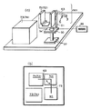
図15は本発明のスペーサの回収方法および回収装置の一実施態様を示す模式図である。図15において、151は硝酸液槽、152は硝酸溶液、153はリアプレートあるいはフェースプレート、154はスペーサ、155はスペーサ収納容器、156はリアプレートあるいはフェースプレートの支持材、157はフリットである。
【0234】
スペーサ154はフェースプレート、リアプレートあるいはその両方に溶着されている場合があるが、ここでは前者の場合について述べる。
【0235】
まず、リアプレート、フェースプレートおよび枠を分離し、フェースプレートとスペーサがフリットで溶着された状態まで分解する。リアプレート、フェースプレート、枠を分離する方法としては、切断する方法、各部材間を溶着しているフリット部に硝酸溶液を噴霧あるいは浸漬してフリットを溶解する方法、加熱によりフリットを溶解する方法などがあるが、スペーサに損傷を与えない点から、硝酸による溶解が望ましい方法と言える。
【0236】
次に、スペーサとフェースプレートを硝酸溶液中に浸漬する。浸漬は、図15に示すように、支持材156でフェースプレート153を支持し、スペーサ154を下向きに浸漬して行う。
【0237】
スペーサ154とフェースプレート153間のフリット157を溶解し、両者を分離するが、この際、スペーサ157が硝酸液層151中に落下し、他のスペーサや周辺部材と接触して損傷を受けないようにするため、図16に示したような収納容器155を用いる。
【0238】
収納容器155は、フェースプレート153とほぼ同じ大きさを有し、スペーサ154の配置に合わせて凹部148が形成されている容器であり、硝酸に対して安定でかつスペーサを損傷する恐れのない材料、例えばフッ素樹脂で形成されている。さらに凹部に液が溜まらないようにするために、容器全体あるいは凹部の底がメッシュ状になっているものでもよい。この収納容器155をスペーサ154の下に配置し、フェースプレート153から分離するスペーサ154が凹部148内に収納されるようにすることで、スペーサ154同士の接触を防ぐことができる。
【0239】
フェースプレート153を除去した後、収納容器155を硝酸液層151から引き上げ、収納容器のまま次の洗浄工程および乾燥工程を行うことができる。
【0240】
なお、スペーサの収納容器155は上記の形状に限ったものではない。図16に示したのは上記で説明した容器の形状の一例であるが、その他にも、図17に示したように、スペーサ154より若干大きい凹型容器149を多数用い、個々の容器149をスペーサの下に配置してフェースプレート153から分離するスペーサ154を収納する方法を用いることもできる。この方法を用いた場合、硝酸液層151から引き上げられた容器149を狭い範囲に収集することができるため、その後の洗浄槽や乾燥槽をより小さくすることができる。
【0241】
図18は本発明のスペーサの回収方法および回収装置の別の実施態様を示す模式図である。図18において、符号151は硝酸液槽、152は硝酸溶液、153はリアプレートあるいはフェースプレート、154はスペーサ、157はフリット、158はリアプレートあるいはフェースプレートの支持台、159はスペーサ支持アーム、160はアーム先端部である。
【0242】
スペーサ154は、リアプレート、フェースプレートおよび枠がそれぞれ分離され、リアプレートあるいはフェースプレートとフリットで溶着された状態まで分解した後、硝酸液槽151中に浸漬される。
【0243】
スペーサ154はフェースプレート、基板あるいはその両方に溶着されている場合があり、本発明はそのいずれの場合でも用いることができるが、ここでは前者の場合について述べる。
【0244】
浸漬の方法は、図18に示したように、まず支持台158上にスペーサ154が上向きになるようにフェースプレート153を置いた後、各々のスペーサ154の上部をアーム159の先端部160で挟み固定する。その後、支持台158を降下させてフェースプレート153および溶着部157を硝酸溶液152中に浸漬する。このようにスペーサ154を予め固定し、フェースプレート153から分離されたスペーサ154が落下しないようにすることで、スペーサ154の損傷を防ぐことができる。なおアーム159およびその先端部160は、硝酸に対して安定な材料、例えばフッ素系化合物で形成されていることが必要である。
【0245】
スペーサ154はアーム先端部160に固定されたまま、次の洗浄工程および乾燥工程を行うことができる。洗浄工程は、スペーサ154上に残ったフリットガラス157を溶解するとともに、フェースプレート153や基板からの溶解物の再付着を除去するものであり、通常新たな硝酸液槽中で行われる。その後、純水槽に移して最終的な洗浄が行われる。
【0246】
さらに乾燥工程においては、上記の純水が揮発する方法であれば何でもよく、例えば温風による乾燥等を用いることができる。
【0247】
なお、乾燥後のスペーサを再利用するにあたっては、スペーサに損傷がないかどうかを検査することが必要である。検査方法は適宜採用されるが、例えば目視により欠陥の有無を確認する方法や加熱による割れの有無を調べる方法等を用いることができる。
【0248】
図19はスペーサ154を示す模式図である。スペーサ154の形状は、通常、長さおよび幅が数10mm、厚み300μm以下の薄い板状であり、絶縁性基材161の表面に帯電防止を目的とした導電膜162が形成されている。このスペーサ154は、目的を達成するのに必要な数だけ、かつ必要な間隔をおいて配置され、フェースプレート153の内側または基板の表面にガラスフリットにより固定されている。尚、スペーサ154は、フェースプレートに固着された場合と同様に、リアプレートに固着されている場合も同様に取り扱われる。
【0249】
導電膜材料としては、例えばクロム、ニッケル、銅等の金属酸化物、アルミと遷移金属合金の窒化物、炭素等が用いられる。
【0250】
スペーサ154の絶縁性基材161としては、例えば石英ガラス、Na等の不純物含有量を減少したガラス、ソーダライムガラスあるいは上述の各種基板上にたとえばSiO2を材料とする絶縁層を積層した基板などを用いることができる。
【0251】
上述のように、スペーサ表面には導電膜162が成膜されており、その材料によって硝酸に対して安定なものと溶解するものがある。硝酸に対して安定な材料が成膜されている場合は、洗浄、乾燥、検査工程を経て再利用することが可能である。一方、硝酸に溶解する材料を用いている場合には、硝酸溶液中で膜を十分溶解し、洗浄、乾燥、検査工程を経た後、導電膜を新たに成膜し再利用することが可能となる。
【0252】
[実施例4]
以下に、実施例を挙げて本発明をさらに詳述する。
【0253】
[実施例4−1]
図15に示した本発明に係るスペーサ回収装置を用いてスペーサの回収を行った。図15の装置は、フェースプレート153とスペーサ154を溶着しているフリットガラス157を溶解し、両者を分離するための装置である。図15において、151は硝酸液槽、152は硝酸溶液、153はフェースプレート、154はスペーサ、155はスペーサ収納容器、156はフェースプレートの支持材、157はフリットガラスである。
【0254】
図20は、本発明に係るスペーサの回収方法の各工程における状態を模式的に示したものである。図20(a)は基板とフェースプレートと枠を分離する工程、(b)はフェースプレートとスペーサを分離する工程、図20(c),図20(d)はスペーサの洗浄工程、図20(e)はスペーサの乾燥工程を表す。
【0255】
この実施例においては、300mm×250mm×2.8mmのソーダライムガラスからなるフェースプレート153に、25枚のスペーサ154が溶着されたディスプレイを用いた。またスペーサ154は、高さ2.8mm、板厚200μm、長さ40mmのソーダライムガラス基材上に導電膜として窒化アルミニウムが約100nmの厚さで成膜されているものを用いた。
【0256】
以下、図15、図16および図20を用いて詳述する。
【0257】
▲1▼ 筐体部を分解し、リアプレート163、フェースプレート153、枠164がフリットガラス157により溶着された部分を取り出した。
【0258】
▲2▼ 上記の溶着部に0.2規定の硝酸溶液を噴出し、溶着部を徐々に溶解し、ほとんどのフリット157が溶解したところでフェースプレート153を支持材156で引き上げて枠部から分離した(図20(a))。
【0259】
▲3▼ 0.2規定の硝酸溶液が入った、長さ400mm、幅350mmの硝酸液槽151中にスペーサを収納するための容器155を沈めた。この容器は図16に示したように、長さ300mm×幅250mm×高さ10mmで、スペーサの配置に合わせて25箇所の凹部(長さ50mm、幅5mm、深さ4mm)が形成されている容器であり、硝酸に対して安定でかつスペーサを損傷する恐れのないフッ素樹脂で形成されている。さらに凹部は、液が溜まらないようにするために、メッシュ状になっている。
【0260】
この硝酸液槽151中に、スペーサ154が溶着された状態のフェースプレート153を、スペーサ154が下向きになるように浸漬し、スペーサ154とフェースプレート153間のフリットを溶解することで両者を分離した。各々のスペーサ154は容器155の凹部内に落下した。
【0261】
スペーサ154と分離されたフェースプレート153を除去した後、容器155を硝酸液槽から引き上げた(図20(b))。
【0262】
▲4▼ スペーサ154を容器155ごと、0.2規定硝酸溶液を収容する洗浄用の硝酸液槽中に沈めた。この工程で、スペーサ154上に残ったフリットガラス157を溶解するとともに、フェースプレート153や基板からの溶解物の再付着を除去した(図20(c))。
【0263】
▲5▼ 次にスペーサ154を容器155ごと純水槽に移して純水165による最終的な洗浄を行った。なお、上記硝酸洗浄槽と純水洗浄槽は、図20(b)の硝酸液槽と同じ大きさのものを用いた(図20(d))。
【0264】
▲6▼ 続いて、スペーサ154に容器155ごと温風166を吹き付け、乾燥を行った(図20(e))。
【0265】
▲7▼ このようにして回収されたスペーサを再利用するにあたり、スペーサ154の検査を行った。検査方法としては、まず光学顕微鏡により導電膜の膜剥がれや、傷、付着物その他の汚れの有無の確認を行った後、加熱による割れの有無を調べガラス基材に欠陥のあるスペーサを除く方法を用いた。これらの検査は、容器に収納されたまま、あるいは個々に取り出して行われた。このようにして検査した結果、不良品として除去されたスペーサは約10%で、ほとんどのスペーサは再利用することが可能となった。良品スペーサはそのまま新たなディスプレイの組み立てに用いられた。
【0266】
[実施例4−2]
本実施例では、実施例4−1と同じ構成のディスプレイを用い、筐体から分離した枠、リアプレート、フェースプレートを切断により分離すること以外は実施例4−1と同様の方法を用いてスペーサの回収を行った。
【0267】
枠、基板、フェースプレートの切断は、図21に示したように、四方の溶着部とその内側、すなわちスペーサのある部分とを分離するように切断した。切断後のスペーサ回収方法は、実施例4−1の工程▲3▼〜▲6▼と同様に行った。
【0268】
このようにして検査した結果、不良品として除去されたスペーサは約15%で、ほとんどのスペーサは再利用することが可能となった。
【0269】
[実施例4−3]
本実施例では実施例1と同じ構成のディスプレイを用い、フェースプレートとスペーサを分離する際に用いるスペーサ収納容器として、図17に示したものを用いる以外は、実施例4−1と同様の方法を用いてスペーサの回収を行った。
【0270】
以下、図15、図16、図17、図22を用いて説明する。
【0271】
実施例4−1の▲1▼〜▲2▼と同様の方法フェースプレートと枠を分離した。
【0272】
▲3▼ 0.2規定の硝酸溶液が入った硝酸液槽中にスペーサ154を収納するための容器167をスペーサと同数の25個、土台168に固定して沈めた。
【0273】
この容器は、図17に示したような、長さ60mm、幅10mm、高さ10mmの長方形であり、上部に長さ50mm、幅5mm、深さ8mmの凹部が形成されている。凹部は液が溜まらないようにするために、メッシュ状になっており、硝酸に対して安定でかつスペーサを損傷する恐れのないフッ素樹脂で形成されている。この容器を各々のスペーサの真下に配置されるよう、台座の上に固定した後、硝酸液槽151中に沈めた。
【0274】
この硝酸液槽151中に、スペーサ154が溶着された状態のフェースプレート153を、スペーサ154が下向きになるよう浸漬し、フリットガラス157を溶解して両者を分離した。各々のスペーサ154は収納容器の凹部内に落下した。
【0275】
スペーサ154と分離されたフェースプレート153を移動した後、容器167を土台168ごと硝酸液槽から引き上げた(図22(a))。
【0276】
▲4▼ 各々の容器を間隔を開けないよう再配置した後、容器ごと0.2規定硝酸溶液を収容する洗浄用の硝酸液槽中に沈めた。この工程で、スペーサ上に残ったフリットガラスを溶解するとともに、フェースプレートや基板からの溶解物の再付着を除去した(図22(b))。
【0277】
▲5▼ 続いて実施例4−1と同様の方法で、純水洗浄、乾燥、検査を行った。なお、本実施例で用いた洗浄槽は、実施例4−1で用いたものよりも小さく、長さ200mm、幅150mmであった(図22(c),(d))。
【0278】
このようにして検査した結果、不良品として除去されたスペーサは約10%で、ほとんどのスペーサは再利用することが可能となった。
【0279】
[実施例4−4]
本実施例では、実施例4−1と同じ装置を用いてスペーサの回収を行った。本実施例においては、実施例4−1と同じフェースプレート25枚のスペーサが溶着されているものを用いた。スペーサは、石英ガラス基材上に導電膜として酸化ニッケルNiO2が成膜されているものを用いた。
【0280】
スペーサの分離、洗浄、乾燥は実施例4−1の▲1▼〜▲6▼と同様の方法で行った。
【0281】
次にこのようにして回収されたスペーサの検査を行った。検査方法としてはまず光学顕微鏡により付着物その他の汚れの確認、導電膜の傷や膜剥がれの確認を行った後、加熱による割れの有無を調べ欠陥のあるスペーサを除く方法を用いた。このようにして検査した結果、不良品として除去されたスペーサは約10%で、ほとんどのスペーサは再利用することが可能となった。良品スペーサはそのまま新たなディスプレイの組み立てに用いられた。
【0282】
[実施例4−5]
本実施例では、実施例4−1と同じ構成のフラットディスプレイを用いた。
【0283】
またスペーサ回収装置として、図18に示したような装置を用いた。図18において、151は硝酸液槽、152は硝酸溶液、153はフェースプレート、154はスペーサ、157はフリット、158はフェースプレートの支持台、159はスペーサ支持アーム、160はその先端部である。150は支持台を支える弾力材であり、支持台158、アーム159には硝酸に対して安定なフッ素樹脂を用い、さらに先端部160にはスペーサを損傷する恐れのないフッ素ゴムを用いた。
【0284】
以下図18、図23を用いて説明する。
【0285】
まず実施例4−1の▲1▼〜▲2▼と同様の方法でフェースプレートと枠を分離した。
【0286】
▲3▼ 支持台158上にスペーサが上向きになるようにフェースプレート153を置いた後、各々のスペーサ154の上部を支持アーム159の先端部160で挟み固定した(図23(a))。その後支持台158を下げてフェースプレート153および溶着部157を0.2規定の硝酸溶液を収容する硝酸液槽151中に浸漬した。フリットガラス157が溶解し、スペーサ154が分離したのを確認した後、硝酸液槽から引き上げた(図23(b))。
【0287】
▲4▼ スペーサを支持材に挟んだままの状態で0.2規定硝酸溶液からなる洗浄用の硝酸液槽中に沈めた。この工程で、スペーサ上に残ってフリットガラスを溶解するとともに、フェースプレートや基板からの溶解物の再付着を除去した(図23(c))。
【0288】
▲5▼ 次に純水槽165に移して最終的な洗浄を行った(図23(d))。
【0289】
▲6▼ 続いて、温風乾燥を行った(図23(e))。
【0290】
▲7▼ このようにして回収されたスペーサを実施例4−1と同様の方法で検査した結果、不良品として除去されたスペーサは約10%で、ほとんどのスペーサは再利用することが可能となった。
【0291】
[実施例4−6]
本実施例では、スペーサが基板およびフェースプレートの両側で溶着されている以外は実施例4−1と同じ構成のディスプレイを用いた。
【0292】
以下、図15、図24を用いて詳述する。
【0293】
▲1▼ 筐体から基板163、フェースプレート153、枠164がフリットガラス157により溶着された部分を取り出した。
【0294】
▲2▼ 実施例4−2と同様の方法で、枠、基板、フェースプレートの溶着部を切断した(図24(a))。
【0295】
▲3▼ 0.2規定の硝酸溶液が入った硝酸液槽151中に基板を下に上記ユニットを徐々に浸漬し、基板とスペーサの溶着部が液中に沈んだところで、それ以上浸漬するのを止めた(図24(b))。
【0296】
このようにして基板とスペーサ間のフリットのみを溶解して分離した(図24(c))。
【0297】
▲4▼ 硝酸液槽から基板を引き上げた後、実施例4−1の工程▲3▼〜▲7▼と同様の方法でスペーサをフェースプレートから分離、回収した。
【0298】
このような方法で回収した結果、不良品として除去されたスペーサは約15%で、ほとんどのスペーサは再利用することが可能となった。
【0299】
[実施形態5]
図25は本発明のディスプレイ装置からの蛍光体の回収方法の工程を示すフローチャートである。図25を参照しつつ、回収工程について説明する。
【0300】
ここで処理・廃棄されるディスプレイ装置(S20)は、フェースプレートに蛍光体が塗布され、電子線の照射や紫外線により蛍光体を発光させる形態のディスプレイで、具体的には通常のCRT及びフラットディスプレイの一部でフェースプレートに蛍光体を塗布されているものが挙げられる。
【0301】
上記のディスプレイ装置は、キャビネットからCRT部またはフラットディスプレイ部を分離する前に、センサによりその機種を識別され、以降の工程で使用されるデータ(例えば寸法、ディスプレイの取り外し方、フェースプレート形状に適したブラシサイズ、形状及び吸引器形状など)がデータベースから引き出される。
【0302】
上記の識別工程で得られたデータに従い、ディスプレイ部をキャビネットから取り出し、更にディスプレイからフェースプレートを外しやすいように、ディスプレイを治具上に固定する。ここで使用される治具は、上記した識別工程で得られたデータに従い、最適な形状の治具が選択され使用される。ディスプレイ部にプラスチック、金属の部材が取り付けられている場合には必要に応じて取り外しを行う(S21)。
【0303】
治具に固定されたディスプレイは、内部の減圧状態を破られて次の工程に送られる。
【0304】
フェースプレートの分離(分解)工程では(S22)、CRTの場合にはフェースプレート部とファンネル部の間、フラットディスプレイの場合にはフェースプレート部と枠部の間にあるフリットガラス部分に沿って、フェースプレート部をディスプレイから取り外す。取り外し方法としては、フェースプレート部とファンネル部の間を切断する、または両部を封着しているフリットガラス部分を剥離液で剥離するなどの方法が挙げられる。CRTの分解方法としては、例えば、電熱線により切断する方法(特開平07−029496号公報)、熱歪みを生じさせて分解する方法(特開平05−151898号公報)、加熱と同時に超音波振動を与えて分解する方法、剥離液として硝酸を使用する方法(特開平07−045198号公報)などが提案されているが、熱歪みの発生を防ぐ、湿式工程には時間とコストがかかるといった理由からワイヤソーまたはエネルギーカッターによる切断が好ましい。またこの際に発生するガラス屑は切断機に付属する吸引器によって吸引除去される。ファンネル部やリアプレートはガラスカレット化される。
【0305】
取り外されたフェースプレートは、内面側を上にした状態で治具上に固定され、ブラシ掃引及び吸引工程に回される(S28)。
【0306】
ブラシ掃引工程は蛍光体の回収のみを目的とするならば、一回の掃引のみで終了することも可能であるが、フェースプレートの再利用も目的とするならば、内面が仕様を満たすまで繰り返し掃引することも可能である。その際、蛍光体を除去するブラシに替え、内面鏡面仕上げ用のバフに変更することもできる。
【0307】
本発明のブラシ掃引工程で使用されるブラシは、通常のCRTの場合にはフェースプレート内面のR(曲率半径)に対応した形状のブラシが選択される、またフラットCRTまたはフラットディスプレイの場合には平面に対応したブラシが選択される。また後述するスリコギ運動方式を採用する場合にはスリコギ運動の分を考慮してフラットなフェースプレートの処理工程でもRのついた曲面形状のブラシを使用する(S32)。
【0308】
本発明で使用されるブラシの運動は、フェースプレート2の表面に対して、単純な回転運動、反復回転運動など特に規定されないが、例えばブラシ171が自転運動と公転運動の両方の運動を同時に行なう方法(図26)、または中心線を自転軸として自転しつつ、自転軸がある一点を中心として回転する運動(スリコギ運動)方法(図27)を採ると、蛍光体の掃出しが容易且つ速やかに行われ、更に内面の平滑化にも役立ち、望ましい。
【0309】
本発明で使用される吸引器はブラシによって掃き出された蛍光体2b及びブラックストライプを吸引回収できる能力を有していればノズル形状、吸引力は特に規定されない。また、蛍光体2bの飛散を防止するためにブラシ内部に設置する、またはブラシの外周を取り囲むように設置することも可能であり、フェースプレート辺部の蛍光体吸引を良好に行なうためにはブラシ内部に設置するのが好ましい。
【0310】
本発明で回収された蛍光体2b及びブラックストライプは、既知の方法によって分離、精製され、特にその手段は問わない。例えば、回収した蛍光体をNaOH,NaClO及びH2O2を含有する水溶液で処理し、次いで弱酸で処理する方法(特開平06−108047号公報)、回収した蛍光体を強酸で処理して希土類を浸出させ、更にシュウ酸を添加して希土類をシュウ酸塩とし、これを焙焼して希土類酸化物を得る方法(特開平08−333641号公報)などが公開されている。
【0311】
以下、フラットディスプレイの一例として、表面伝導型電子放出素子を用いたフラットディスプレイ装置の構成例について説明する。図29は、スペーサを用いたディスプレイ装置の斜視図であり、内部構造を示すためにパネルの1部を切り欠いて示している。
【0312】
図29において、11は電子放出素子部、1はリアプレート、3は側壁(枠)
、2はフェースプレートであり、リアプレート1、側壁3、フェースプレート2により表示パネルの内部を真空に維持するための気密容器(外囲器15)を形成している。スペーサ4は必要に応じて設けられるもので、大気圧を受けて外囲器が破損、変形するのを防止する等の目的から設けられる。気密容器を組み立てるにあたっては、各部材の接合部に十分な強度と気密性を保持させるため封着する必要があるが、たとえばフリットガラスを接合部に塗布し、大気中あるいは窒素雰囲気中で、摂氏400〜500度で10分以上焼成することにより封着する。
【0313】
リアプレート1には、基板41が固定されているが、該基板上には冷陰極型電
子放出素子11がN×M個形成されている(N,Mは2以上の正の整数であり、目的とする表示画素数に応じて適宜設定される。たとえば、高品位テレビジョンの表示を目的とした画像形成装置においては、N=3000,M=1000以上の数を設定することが望ましい。)。N×M個の冷陰極型電子放出素子11は、M本のX方向配線12とN本のY方向配線13により単純マトリクス配線されている。
【0314】
ここでは、気密容器のリアプレート1にマルチ電子ビーム源の基板41を固定する構成としたが、マルチ電子ビーム源の基板41が十分な強度を有するものである場合には、気密容器のリアプレート1としてマルチ電子ビーム源の基板41自体を用いてもよい。
【0315】
また、フェースプレート2の下面には、蛍光膜2bが形成されている。カラー
のディスプレイの場合には、蛍光膜2bの部分にはCRTの分野で用いられる赤、緑、青、の3原色の蛍光体が塗り分けられている。各蛍光体間にはブラックストライプが設けてある。ブラックストライプを設ける目的は、電子ビームの照射位置に多少のずれがあっても表示色にずれが生じないようにすることや、外光の反射を防止して表示コントラストの低下を防ぐことなどである。
【0316】
なお、モノクロームの表示パネルを作成する場合には、単色の蛍光体材料を蛍
光膜2bに用いればよく、またブラックストライプを必ずしも用いなくともよい。
【0317】
また、蛍光膜2bのリアプレート側の面には、CRTの分野では公知のメタル
バック2cを設けてある。メタルバック2cを設けた目的は、蛍光膜2bが発する光の一部を鏡面反射して光利用率を向上させることや、負イオンの衝突から蛍光膜2bを保護することや、電子ビーム加速電圧を印加するための電極として作用させることや、蛍光膜2bを励起した電子の導電路として作用させることなどである。メタルバック2cは、蛍光膜2bをフェースプレート基板2a上に形成した後、蛍光膜表面を平滑化処理し、その上にAlを真空蒸着する方法により形成した。なお、蛍光膜2bに低加速電圧用の蛍光体材料を用いた場合には、メタルバック2cは用いない場合がある。
【0318】
また、加速電圧の印加用や蛍光膜の導電性向上等を目的として、フェースプレ
ート基板2aと蛍光膜2bとの間に、たとえばITOを材料とする透明電極を設けることもある。
【0319】
また、Dx1〜DxmおよびDy1〜DynおよびHvは、当該表示パネルと不図示の
電気回路とを電気的に接続するために設けた気密構造の電気接続用端子である。Dx1〜Dxmはマルチ電子ビーム源のX方向配線と、Dy1〜Dynはマルチ電子ビー ム源のY方向配線と、Hvはフェースプレートのメタルバック2cと電気的に接続している。
【0320】
[実施例5]
以下、本発明の実施例について図面を用いて詳細に説明する。
【0321】
[実施例5−1]
フェースプレート部、枠部及びリアプレート部よりなる表面伝導型電子放出素子を用いる方式のフラットディスプレイ装置を、フェースプレート側を下にして治具上に固定し、ゴム吸盤を備えた押え具をリアプレート部に密着させ、ディスプレイを固定した。排気管先端を砕いてディスプレイ内の真空状態を解き、フェースプレート部と枠部の間のフリット部分をエネルギーカッターにより切りとり分解した。
【0322】
リアプレート部及び枠部を取り除き、吸引器を備えスリコギ運動をする回転ブラシ(図27参照)により、フェースプレート2内面を掃引して蛍光体2bを掃き出しつつ(約20分間)、蛍光体2b及びブラックマトリックスを吸引孔172より吸引回収した。
【0323】
蛍光体2bが完全に除去されてから、更に30分間内面を磨き、鏡面化処理を行なった。
【0324】
フェースプレート内面のブラックマトリックス部と蛍光体2b塗布部の凸凹は15μm以下に抑えられており、そのまま再生フェースプレートとして使用できることがわかった。
【0325】
[比較例5−1]
実施例5−1と同様にして、分解されたフェースプレートをシュウ酸水溶液に浸漬し蛍光体を除いた後、ブラックマトリックスを高圧水にて除いた。蛍光体塗布部とブラックマトリックス塗布部では約85μmの凸凹が観察された。
【0326】
[実施例5−2]
キャビネットから分離したCRTから、電子銃及び偏向ヨーク部分を切り取った。CRTのフェースプレート側を下にして治具上に固定し、ゴム吸盤を備えた押え具をファンネル部に密着させ、CRTを固定した。CRTのフリットガラス部に巻かれた防爆バンドを剥がし取り、更に粘着剤をグラインド操作により除いた。CRTをエネルギーカッターによりフェースプレート部とファンネル部に分解した。
【0327】
ファンネル部を取り除き、吸引器を備えた公転運動ブラシ(図26及び図28参照)により、フェースプレート内面を掃引して蛍光体を掃き出しつつ(約20分間)、蛍光体及びブラックトマリックスを吸引回収した。
【0328】
蛍光体が完全に除去されてから、回転ブラシをバフに変更して、更に30分間内面を磨き、鏡面化処理を行なった。
【0329】
フェースプレート内面のブラックマトリックス部と蛍光体塗布部の凸凹は10μm以下に抑えられており、そのまま再生フェースプレートとして使用できることがわかった。
【0330】
図28(a),(b)はブラシ及び吸引器の構成を示す断面図である。図28
(a)はブラシ部171内に吸引孔が設けられ、吸引機構173により吸引が行われる。図28(b)はブラシ部171を吸引器174で覆い、吸引を行うとともに、吸引による空気の流れをタービン175で回転運動に変え、ブラシ部171の駆動力として使用する。
【0331】
[実施形態6]
以下、本発明による実施形態について、図面を参照しつつ詳細に説明する。本実施形態では、上述したフェースプレートや、リアプレート、枠、スペーサ等を回収しようとする場合、まず、FPD内部の気密容器によって10−5Pa程度の真空に近い低気圧であるので、通常の気圧に戻す必要がある。その場合、気圧を戻さずに、直接破削、融解等で処理すれば、効率のよい回収ができない。そこで、リサイクルも可能な回収方法の一工程として、真空気密容器から通常気圧に戻す方式を、以下に説明する。
【0332】
図30は、本発明の画像表示装置の一実施形態を示す模式図である。図中、201は画像表示部、202は画像表示装置の圧力を維持する気密容器、203は該気密容器内部に有り、該気密容器を安定に保つ耐大気圧構成部材、204は前記圧力を得るために排気装置に接続する手段、205は該気密容器内を徐々に大気圧に戻す手段である。
【0333】
また、図31は、本発明の画像表示装置の実施形態の一例を示すFPDの模式図である。図中、2は画像表示部であるフェースプレートであり、ガラス基板2a、蛍光面2b、メタルバック2cからなっている。1はリアプレート、3は枠である。これらのフェースプレート2、リアプレート1、枠3によって気密容器202が構成される。また、図30に示した排気装置に接続する手段204と大気圧に戻す手段205とが備えられている。また、耐大気圧構成部材の一例としてスペーサ4が備えられている。
【0334】
本発明に好適な画像表示装置としては、内部が大気圧より低圧力を維持する表示装置である。例えば、CRTをはじめとする画像表示装置、プラズマディスプレイパネル(PDP)、表面伝導型電子放出素子を含む平面型画像表示装置、電界(FE)型電子放出素子を含む平面型画像表示装置、メタル−絶縁物−メタル(MIM)型電子放出素子を含む平面型画像表示装置、蛍光表示管、フラットCRT、薄型のFPD等が該当する。
【0335】
CRTをはじめとする画像表示装置の画像表示部15は、液晶表示装置やエレクトロルミネッセンス型パネルに対して、通常の大気圧に比べ、かなり低い圧力に保たれている。これは、電子を微細な蛍光体等に照射し、発光させ、これを制御することによって画像情報を表示しているためである。すなわち、圧力を低くし、電子がぶつかる障害となる物質を十分排除した雰囲気にしなければ、電子の軌道を制御することができないからである。この様な電子の軌道を制御できる圧力としては、画像表示装置の構成によって、適宜最適な圧力が選ばれるが、10Pa以下がよい。好ましくは1Pa以下の圧力が望ましい。
【0336】
画像表示部15の内部圧力を維持する気密容器の材料としては、フェースプレート2aには内部の画像情報を外部に表示できる可視光に対して透明で、かつ内部圧力を維持できる強度を持つ材料、主として各種ガラス材料が用いられる。また、フェースプレート2aと枠3、リアプレート1とは内部を気密に維持するため、ほぼ同一の熱膨張係数を備え、ほぼ同一の熱膨張係数を有するフリットガラス等で封着できる材料が好ましい。
【0337】
また、内部圧力が外部の大気圧に比べて差が大きい場合、気密容器202の強度を向上させ、気密容器202の変形を防ぐために、スペーサ4等の耐大気圧構成部材が用いられる。特に大画面の画像表示装置では、気密容器202を厚くすることで容器の強度をあげようとすると、画像表示装置の重量が増加し、家庭での使用が困難になる。
【0338】
従って、画像表示装置の軽量化をはかるために、気密容器202の外壁以外にも、耐大気圧構成部材が用いられる。また、薄型のFPDでは、気密容器202を構成するパネル内部の画像表示部1であるフェースプレート2と、リアプレート1の間隔を一定にすることで画像表示装置の全面にわたって均一な画像を得る事ができる。そこで、耐大気圧構成部材としてスペーサ4がパネル内部に多数配置され気密容器202であるパネル内のフェースプレート2とリアプレート1間の距離をほぼ一定に保っている。
【0339】
このスペーサ4は、パネルが大きくなるにしたがって、フェースプレート2とリアプレート1の歪みを押さえるため、パネル内のより多くの場所に用いなければならない。形状、枚数などは、フェースプレート2とリアプレート1の大きさ、強度、距離ならびに枠3の強度等によって適宜決められる。
【0340】
この様な構成の画像表示部を持つ気密容器202は、真空ポンプ等の排気装置に接続する手段204を有することで気密容器202内部の圧力を低くすることができる。十分に低い圧力になるまで排気した後、封着することで気密容器15内部を低い圧力に保つことができる。その後、画像表示装置の画像表示部を駆動する。
【0341】
気密容器202につながる後は、徐々に大気圧に戻す手段である。通常、リークする時の流れる気体の量Qは、以下の式で表される。
【0342】
Q=C(P1 −P0 ) [Pa・m2 /s]…………(1)
ここで、
C:コンダクタンス[m2 /s]
P1 :大気圧 [Pa]
P0 :気密容器内部の圧力[Pa]
P1 −P0 :大気圧と気密容器内部の圧力差[Pa]
である。
【0343】
気密容器や内部構成部材の破損を防止するには、気密容器内部への急激な気体流入を防ぐことが重要である。このためには気体の流量Qを101 Pa・m2 /s程度以下にすることが望ましい。従って、(1)式より、コンダクタンスCが、10−4m2 /s程度以下のリーク手段を持つ機構を、徐々に大気圧に戻す手段205として、気密容器202に配置する。
【0344】
この様な徐々に大気圧に戻す手段205としては、スローリーク弁、仕様に応じた長い細管を気密容器に設けたり、多孔質材料を用いることなどで行う。さらに、この徐々に大気圧に戻す手段205は、気密容器202と大気側をつなぐ位置に配置されるが、大気側からも排気装置に接続し封着する。こうすることで気密容器202を低圧力に保つ時は大気側からも密閉される。画像表示装置を再利用するためリークする時は大気側の封着を解除し、気密容器内の圧力を徐々に大気圧にすることができる。
【0345】
また、本実施形態では、徐々に大気圧に戻す手段205を気密容器202の一辺に設ける例を示したが、これに限られるものではなく、気密容器202のコーナーや裏面、側面等、画像表示部1を妨げない位置に配置すれば良い。
【0346】
必要に応じてフィルター等を設け、ガスを徐々に導入する機構に接続することも、可能である。
【0347】
使用済み画像表示装置を再利用する場合には、その後の処理に応じて不活性ガス、窒素、空気、水分を取り除いた空気等を徐々に導入する。
【0348】
また、製造工程中に発生した不良を修理する場合は、その後の製造工程に支障を及ぼさないよう適宜導入ガスを選択し、低い圧力に保たれた気密容器202を徐々に大気圧に戻し、分解、修理を行う。
【0349】
[実施例6]
以下、実施例を挙げて、本発明を詳述する。
【0350】
[実施例6−1]
図30、図31を参照しながら実施例1を説明する。図30は本発明の画像表示装置の構成を示す図である。図31は本発明の画像表示装置でFPDの例である。
【0351】
画像表示部であるフェースプレート2とリアプレート1、枠3からなる気密容器202内には耐大気圧構成部材であるスペーサ214が配置されている。気密容器202には、排気装置に接続する排気接続手段204がつながっており、内部を低圧力に保った後、封着されている。本実施例では5×10⁻²Pa程度まで排気後封着した。さらに気密容器202には、徐々に大気圧に戻す気圧戻し手段205がつながっている。本実施例ではコンダクタンスCが約10−7m2 /s程度のスローリーク弁を用いた。このスローリーク弁は、大気側も5×10−2Pa程度まで排気した後、封着している。この画像表示装置を分解するため、徐々に大気圧に戻す手段205の大気側を破り、気密容器202をリークした。分解、解体後パネル内を確認したところ、スペーサ4の破損も無く、特に気密容器202内の部材に傷がついた形跡も無かった。
【0352】
次に比較のため、同様の画像表示装置の排気装置に接続する排気接続手段204を破り気密容器202をリークした。すぐにパネル内は大気圧に開放されたが、内部のスペーサ4は破損し、その破片がフェースプレート2、リアプレート1、枠3にたくさんの傷を付けていた。
【0353】
[実施例6−2]
本実施例では、画像表示装置として、図32に示すようなマトリックス駆動方式の表面伝導型電子源ディスプレイ(SED)の例を示す。リアプレート1の上には表面伝導型電子源の電子源11を駆動するための配線12、13が形成されている。配線12、配線13はそれぞれX方向(Dox1,Dox2,…Doxm)およびY方向(Doy1,Doy2,…Doyn)の素子配線である。このSEDは、図31に示すようなスペーサ214を含む構造を有している。本実施例も実施例6−1と同様、徐々に大気圧に戻す気圧戻し手段205を有している。
【0354】
パネル部がほぼ完成した後駆動したところ、パネル内の一部に欠陥があることが判明した。そこで、徐々に大気圧に戻す気圧戻し手段205の大気側を開放し、パネルをリークし、欠陥を修理した。その後、再度排気装置に接続する排気接続手段204からパネル内を排気封着、同時に徐々に大気圧に戻す気圧戻し手段205の大気側を排気封着を行い、画像表示装置を完成した。駆動させ、画像を表示させたところ、欠陥は、修理されており、他の欠陥も発生していなかった。
【0355】
[実施形態7]
以下、本発明の実施形態7について、図面を参照しつつ説明する。
【0356】
図33(a)は本発明のフラットディスプレイの一態様を模式的に示した断面図、図33(b)は図33(a)に示したフラットディスプレイの一部を切り欠いて見た平面図である。
【0357】
本発明のフラットディスプレイは、ガラス基板上に多数の電子放出素子221が配置されたリアプレート222と、該リアプレート222に対向して配置され画像表示部223が設けられたフェースプレート224と、支持枠225と、該リアプレート222と該フェースプレート224との間隔を大気圧に対して保持するためのスペーサ226とを少なくとも有し、かつこれらをフリットガラス229を用いて気密接合することにより構成されている。フリットガラス229は一般に酸化鉛等を主成分とする低融点ガラスである。
【0358】
各部材の接合において、スペーサと基板との接合には第1のフリットガラス227が用いられ、リアプレートと支持枠の接合には第2のフリットガラス228、フェースプレートと支持枠の接合には第3のフリットガラス229が用いられる。上記3種類のうちフリットガラス228と229は軟化温度が異なり、スペーサ226を接合している第1のフリットガラス227は第2、第3のフリットガラス228、229のうち、より軟化温度の高いものと同じあるいはそれ以上の高い軟化温度を有する。いずれも350〜470℃の範囲にあり、他フリットガラスに対しては20℃以上異なることが好ましい。
【0359】
上記複数のフリットガラスうち、第2、第3のフリットガラス228、229については、どちらの軟化温度が高くてもよく、工程上の問題である。またスペーサ226はリアプレート222またはフェースプレート224のいずれか一方の基板に接合されており、それはどちらの基板であってもよい。
【0360】
製造工程における各部材の接合は、接合部にフリットガラスを塗布し、フリットの軟化温度以上に加熱して行う。実際の操作としては、大気中で300℃程度の加熱処理を行い、フリットガラス中にバインダーとして含まれる成分を除去(この工程を仮焼成とよぶ)した後、Ar等の不活性ガス中で400℃以上の加熱処理を行い接合部を溶着する。各部材の接合で、手順はどのようであっても構わず、上記複数のフリットを同時に塗布し、全てのフリットの軟化温度以上にまで加熱して一度に接合を行うことも可能である。また軟化温度の高いフリットを用いる箇所から順に接合する方法を用いることもできる。この方法は先に接合した箇所のフリットガラスを溶融しない温度で順に接合することができるため、好ましい方法といえる。
【0361】
本発明でいう軟化温度とは、フリットガラスの粘度が107.65dPa・s(Poise)に相当する温度であり、軟化温度より高い温度(焼成温度)で加熱することにより接合することができる。
【0362】
スペーサの形状は、通常長さ及び幅が数10mm、厚み300μm以下の薄い板状であり、絶縁性基材の表面に帯電防止を目的とした導電膜が形成されている。このスペーサは目的を達成するのに必要な数だけ、かつ必要な間隔をおいて配置される。
【0363】
スペーサの絶縁性部材としては、例えば石英ガラス、Na等の不純物含有量を減少したガラス、ソーダライムガラスあるいは上述の各種基板上にたとえばSiO2を材料とする絶縁層を積層した基板などを用いることができる。
【0364】
導電膜材料としては例えばクロム、ニッケル、銅等の金属酸化物、アルミと遷移金属合金の窒化物、炭素等が用いられる。
【0365】
続いて、フェースプレート224の構成について説明する。図33において、フェースプレート224は、ガラス基板上に蛍光膜230、メタルバック231が形成されてなり、この部分は画像表示領域となる。蛍光膜230は白黒画像の表示装置の場合には、蛍光体のみからなるが、カラー画像を表示する場合には、赤、緑、青の3原色の蛍光体により画像形成単位(以下、ピクセルとも呼ぶ)が形成され、その間を黒色導電材で分離した構造とする場合がある。黒色導電材はその形状により、ブラックストライプ、ブラックマトリクスなどと呼ばれる。メタルバック231はAl等の導電性薄膜により構成される。メタルバック231は、蛍光体から発生した光のうち、電子放出素子群221からなる電子源の方に進む光をガラス基体の方向に反射して輝度を向上させるとともに、パネル内に残留したガスが、電子線により電離され生成したイオンの衝撃によって、蛍光体が損傷を受けるのを防止する働きもある。
【0366】
また、フェースプレート224の画像表示領域に導電性を与えて、電荷が蓄積されるのを防ぎ、電子源に対してアノード電極の役割を果たすものである。尚、メタルバック231は高圧端子Hvと電気的に接続されており、高圧端子Hvを通して外部から電圧を印加できるようになっている。
【0367】
次に本発明のフラットディスプレイの解体方法について説明する。
【0368】
図34は本発明の解体方法の一態様を示す模式図である。図34において、222はリアプレート、224はフェースプレート、225は支持枠、226はスペーサ、227は第1のフリットガラス、228は第2のフリットガラス、229は第3のフリットガラスを示す。図34において、各接合部に用いられている第1、第2及び第3のフリットガラスには軟化温度の異なる3種類のフリットガラスが用いられている(図34(a))。ここではその一態様として軟化温度が高い順に第1のフリットガラス227>第2のフリットガラス228>第3のフリットガラス229であるとする。
【0369】
解体手順は以下の通りである。まずパネルを適当な加熱炉中に入れ、第3のフリットガラス229の軟化温度以上かつそれ以外のフリットの軟化温度以下に加熱し、第3のフリットガラス229のみを溶融する。温度を保持しながらフェースプレート224を支持枠225から分離する(図34(b))。次に第2のフリットガラス228の軟化温度以上かつ第1のフリットガラス227の軟化温度以下まで加熱温度を上昇させる。第2のフリットガラス228が溶融したところで支持枠225とリアプレート222を分離する(図34(c))。さらに加熱温度を上昇させて第1のフリットガラス227を溶融し、スペーサ226とリアプレート222を分離する。
【0370】
なお、第1のフリットガラス227による接合部において分離する方法としては特に加熱による方法を用いなくてもよい。たとえば図35に示したように、図34(c)の状態まで分離した後は、このパネルをフリットを溶解する溶液中239に浸漬し、フリットガラスを溶解させて両者を分離することも可能である。溶液としては硝酸が好ましく用いられる。
【0371】
分離後の各部材は硝酸等により残留フリットガラスを除去し、さらに洗浄工程を経て回収される。回収後の部材は、再利用工程またはより細かな回収工程へと進む。
【0372】
図36は本発明の解体方法の別の一態様を示す模式図である。図36においても、各接合部には軟化温度の異なる3種類のフリットガラスが用いられている(図36(a))。ここではその一態様として軟化温度が高い順に第1のフリットガラス227>第3のフリットガラス229>第2のフリットガラス228であるとする。
【0373】
解体手順は以下の通りである。まずパネルを適当な加熱炉中に入れ、第2フリットガラス228の軟化温度以上かつそれ以外のフリットガラスの軟化温度以下に加熱し、第2のフリットガラス228のみを溶融する。加熱しながらフェースプレート224と支持枠225及びリアプレート222とスペーサ226に分離する(図36(b))。前者については次の工程で加熱温度を第2のフリットガラス228の軟化温度以上にする。すると第2のフリットガラス228が溶融するので支持枠225とリアプレート222を分離する(図36(c))。またリアプレート222とスペーサ226の分離については、上記第1の実施態様と同様の方法で行うことができる。
【0374】
[実施例7]
実施例を挙げて本発明をさらに詳述する。なお本実施例中では、以下の表1に示したフリットガラスの中から適宜選択して用いた。
【0375】
【表1】

[実施例7−1]
図33(a)は本発明のフラットディスプレイの一態様を模式的に示した断面図、図33(b)は図33(a)に示したフラットディスプレイの一部を切り欠いて見た平面図である。本発明のフラットディスプレイは、ガラス基体上に多数の電子放出素子221が配置されたリアプレート222と、該リアプレート222に対向して配置され画像表示部223が設けられたフェースプレート224と、支持枠225と、該リアプレート222と該フェースプレート224との間隔を大気圧に対して保持するためのスペーサ226とを少なくとも有し、かつこれらをフリットガラスを用いて気密接合することにより構成されている。
【0377】
本実施例においては、300mm×250mm×2.8mmのソーダライムガラスからなるリアプレート222に、25枚のスペーサ226が溶着されたディスプレイを作製した。またスペーサは、高さ2.8mm、板厚200μm、長さ40mmのソーダライムガラス基材上に導電膜として窒化アルミニウムが約100nm成膜されているものを用いた。
【0378】
スペーサ226とリアプレート222間のフリットガラス227としては表1−III (軟化温度410℃)を用いた。またリアプレート222と支持枠225間のフリットガラス228には表1−II(軟化温度390℃)、フェースプレート224と支持枠225間のフリットガラス229には表1−I(軟化温度365℃)のフリットガラス229を用いた。
【0379】
また電子放出素子221として、図37に示したタイプの表面伝導型電子放出素子を作製した。
【0380】
次に本実施例におけるフラットディスプレイの製造方法を図33、図37、図38を用いて説明する。
▲1▼まずリアプレートとしてソーダライムガラスを用い、該基板上にPtを用いて素子電極235,236を作製した。この時、素子電極間隔L1を10μm、素子電極幅W1を500μm、素子電極の厚さdを100nmとした。次に素子電極上を含む所望の位置に有機パラジウム含有溶液を塗布した後、300℃で10分間の加熱処理を行い、酸化パラジウム(PdO)微粒子(平均粒径7nm)からなる微粒子膜234を形成した。
【0381】
以上のようにして基板上に複数の電子放出素子221を作製してリアプレート222を得た。またフェースプレートはガラス基板に画像形成部材223として蛍光体を塗布したものを用いた。
▲2▼次に本実施例における封着方法を説明する。まず、スペーサ226をフリットガラスIII (軟化温度410℃)でリアプレート222に溶着した(図38(a))。
▲3▼次にフリットガラスII(軟化温度390℃)をリアプレート222上の外周部分(図33(b)のフリット塗布箇所240の部分)に塗布し、またフェースプレート224上の同部分にフリットガラスI(軟化温度365℃)を塗布した後、フェースプレート224、支持枠225、リアプレート222を精密な位置合わせを行いながら重ね合わせた(図38(b))。フェースプレート224とリアプレート222が動かないように治具を用いて固定し、炉の中で400℃で10分以上焼成した。
【0382】
このようにして、フェースプレート、リアプレート、支持枠を接合した(図38(c))。
▲4▼次に、上記工程で作製された容器内を真空状態にするために、封着処理後支持枠225等に設けられた排気管(不図示)により真空に引き、その後排気管を封止した。
【0383】
[実施例7−2]
本実施例では実施例7−1と同じ構成のディスプレイを作製した。本実施例においてはスペーサはリアプレートに接合されており、その接合にはフリットガラスIII(軟化温度410℃)を用いた。またリアプレート222と支持枠225の接合にはフリットガラスI(軟化温度365℃)、フェースプレート224と支持枠225の接合にはフリットガラスII(軟化温度390℃)を用いた。
【0384】
本実施例におけるフラットディスプレイの製造は実施例7−1と同様の方法を用いた。
【0385】
[実施例7−3]
本実施例では実施例7−1と同じ構成のディスプレイを作製した。本実施例においてはスペーサ226はリアプレート222に接合されており、その接合にはフリットガラスIV(軟化温度450℃)を用いた。またリアプレート222と支持枠225の接合にはフリットガラスIII (軟化温度410℃)、フェースプレート224と支持枠225の接合にはフリットガラスII(軟化温度390℃)を用いた。
【0386】
本実施例のフラットディスプレイにおけるリアプレート222及びフェースプレート224の製造は実施例7−1の▲1▼と同様の方法を用いた。
▲2▼次に本実施例における封着方法を説明する。まず、スペーサ226をフリットガラスIV(軟化温度450℃)でリアプレート222に溶着した(図38(a))。
▲3▼次にフリットガラスIII(軟化温度410℃)をリアプレート222上の外周部分(図33(b)240の部分)に塗布し、またフェースプレート224上の同部分にフリットガラスII(軟化温度390℃)を塗布した後、フェースプレート224、支持リアプレート222を精密な位置合わせを行いながら重ね合わせた(図38(b))。フェースプレート224とリアプレート222が動かないように治具を用いて固定し、炉の中で420℃で10分以上焼成した。
【0387】
このようにして、フェースプレート224、リアプレート222、支持枠225を接合した(図38(c))。
▲4▼次に、上記工程で作製された容器内を真空状態にするために、封着処理後支持枠225等に設けられた排気管(不図示)により真空に引き、その後排気管を封止した。
【0388】
[実施例7−4]
本実施例では実施例7−1と同じ構成のディスプレイを作製した。本実施例においては、スペーサ226はフェースプレート224に接合されており、その接合にはフリットガラスIII (軟化温度410℃)を用いた。またリアプレート222と支持枠225の接合にはフリットガラスII(軟化温度390℃)、フェースプレート224と支持枠225の接合にはフリットガラスI(軟化温度365℃)を用いた。
【0389】
本実施例のフラットディスプレイにおけるリアプレート222及びフェースプレート224の製造は実施例7−1の▲1▼と同様の方法を用いた。
▲2▼次に本実施例における封着方法を、図39を用いて説明する。まず、スペーサ226をフリットガラスIII (軟化温度410℃)でフェースプレート224に溶着した(図39(a))。
▲3▼次にフリットガラスII(軟化温度390℃)をリアプレート222上の外周部分に塗布し、またフェースプレート上の同部分にフリットガラスI(軟化温度365℃)を塗布した後、フェースプレート224、支持枠225、リアプレート222を精密な位置合わせを行いながら重ね合わせた(図39(b))。フェースプレート224とリアプレート222が動かないように治具を用いて固定し、炉の中で420℃で10分以上焼成した。
【0390】
このようにしてフェースプレート224、リアプレート222、支持枠225を接合した(図39(c))。
▲4▼次に、上記工程で作製された容器内を真空状態にするために、封着処理後支持枠225等に設けられた排気管(不図示)により真空に引き、その後排気管を封止した。
【0391】
[実施例7−5]
本実施例では実施例7−1と同じ構成のディスプレイを作製した。本実施例においては、スペーサ226はリアプレート222に接合されており、その接合にはフリットガラスII(軟化温度390℃)を用いた。またリアプレート222と支持枠225の接合にもフリットガラスII(軟化温度390℃)、フェースプレート224と支持枠225の接合にはフリットガラスI(軟化温度365℃)を用いた。
【0392】
本実施例のフラットディスプレイにおけるリアプレート222及びフェースプレート224の製造は実施例7−1の▲1▼と同様の方法を用いた。
▲2▼次に本実施例における封着方法を、図40を用いて説明する。まず、スペーサ226と支持枠225をフリットガラスII(軟化温度390℃)でリアプレート222に溶着した(図40(a))。
▲3▼次にフリットガラスI(軟化温度365℃)をフェースプレート224上の外周部分に塗布した後、フェースプレート224と支持枠225を精密な位置合わせを行いながら重ね合わせた(図40(b))。フェースプレート224と支持枠が動かないように治具を用いて固定し、炉の中で420℃で10分以上焼成した。
【0393】
このようにしてフェースプレート224と支持枠225を接合した(図40(c))。
▲4▼次に、上記工程で作製された容器内を真空状態にするために、封着処理後支持枠225等に設けられた排気管(不図示)により真空に引き、その後排気管を封止した。
【0394】
[実施例7−6]
本実施例では、実施例7−1に示したフラットディスプレイの解体方法について述べる。図34を用いて解体方法を説明する。
▲1▼まず排気管の封止箇所を破って空気を導入し、容器内の真空を解除した(不図示)。
▲2▼次にディスプレイを加熱炉の中に入れ、リアプレート222及びフェースプレート224を適当な治具で保持した後、380℃に加熱した。365℃を越えたところでフェースプレート224と支持枠225を接合していたフリットガラスIが徐々に溶融し、フェースプレート224を保持している治具を上部に引き上げることで両者を分離した(図34(a),(b))。
▲3▼次に、支持枠225を適当な治具で保持した後、加熱温度を400℃に上昇させた。390℃を越えたところでリアプレート222と支持枠225を接合していたフリットガラスIIが徐々に溶融し、支持枠225を保持している治具を上部に引き上げることで両者を分離した(図34(c))。
▲4▼引き続き各スペーサ226を適当な治具で保持した後、加熱温度を450℃に上昇させた。410℃を越えたところでリアプレート222とスペーサ226を接合していたフリットガラスIIIが徐々に溶融し、スペーサ226を保持している治具を上部に引き上げることで両者を分離した(図34(d))。
【0395】
回収後の各部材は0.2規定硝酸液で洗浄し残留フリットガラスを除去した後、洗浄、乾燥を行った。その後、スペーサ及び支持枠は検査工程を経て選別され、損傷のなかったものはそのまま再利用工程へと進んだ。またリアプレート及びフェースプレートは、該基板上に形成された各資源の回収工程、さらに基板自体の再利用工程等へと進んだ。本実施例に従って解体を行ったフラットディスプレイにおいては、工程中でのフェースプレート222、リアプレート224、支持枠及びスペーサ226の破損はほとんどなかった。
【0396】
[実施例7−7]
本実施例では、実施例7−2に示したフラットディスプレイの解体方法について述べる。図36を用いて解体方法を説明する。
▲1▼まず排気管の封止箇所を破って空気を導入し、容器内の真空を解除した(不図示)。
▲2▼次にディスプレイを加熱炉の中に入れ、リアプレート222及びフェースプレート224を適当な治具で保持した後、380℃に加熱した。365℃を越えたところでリアプレート222と支持枠225を接合していたフリットガラスIが徐々に溶融し、フェースプレート224を保持している治具を上部に引き上げることでフェースプレート224と支持枠225及びリアプレート222とスペーサ226の2つの部分に分離した(図36(a),(b),(c))。
▲3▼分離した2つの部分のうち、フェースプレート224と支持枠225については実施例7−5の方法と同様に炉を410℃まで加熱させてフリットガラスIIを徐々に溶融し、支持枠225を保持している治具を上部に引き上げることで両者を分離した(図36(e))。
▲4▼一方、リアプレート222とスペーサ226の分離は実施例7−5の▲4▼と同様の方法で行った(図36(d))。回収後の各部材は0.2規定硝酸液で洗浄し残留フリットガラスを除去し、洗浄、乾燥を行った。その後、スペーサ226及び支持枠は検査工程を経て選別され、損傷のなかったものはそのまま再利用工程へと進んだ。またリアプレート222及びフェースプレート224は、該基板上に形成された各資源の回収工程、さらに基板自体の再利用工程等へと進んだ。本実施例に従って解体を行ったフラットディスプレイにおいては、工程中でのフェースプレート、リアプレート、支持枠及びスペーサの破損はほとんどなかった。
【0397】
[実施例7−8]
本実施例では、実施例7−3に示したフラットディスプレイの解体方法について述べる。図34,図35を用いて解体方法を説明する。
【0398】
まず実施例7−6の▲1▼〜▲3▼の方法で、ディスプレイからフェースプレート224および支持枠225を図34(c)の状態まで分離した。
▲4▼次にリアプレートを適当な治具で保持し、リアプレート222とスペーサ226の接合部を0.2規定の硝酸液239が入った液槽237に浸漬した(図35(a))。硝酸液槽237はその内部に網目状のテフロン(登録商標)製の容器238を有している。接合部を硝酸液239に浸漬するとフリットガラスIVが溶解しスペーサ226は容器238中に回収された。全てのスペーサ226が分離したのを確認した後、リアプレート222を引き上げた(図35(b))。またスペーサ226も容器238ごと硝酸液239から引き上げた。
【0399】
回収後の各部材は残留フリットガラスを除去し、洗浄、乾燥を行った。その後、部材毎に検査工程を経て選別され、再利用工程あるいはより細かな回収工程へと進んだ。本実施例に従って解体を行ったフラットディスプレイにおいては、工程中でのフェースプレート、リアプレート、支持枠及びスペーサの破損はほとんどなかった。
【0400】
[実施例7−9]
本実施例では、実施例7−4に示したフラットディスプレイの解体方法について述べる。まず実施例7−7の▲1▼〜▲2▼と同様の方法でディスプレイを360℃に加熱し、リアプレート222と支持枠225及びフェースプレート224とスペーサ226の2つの部分に分離した。
【0401】
次に分離した2つの部分のうち、リアプレート222と支持枠225は実施例7−7の▲3▼と同様の方法で分離した。
【0402】
一方、フェースプレート224とスペーサ226の分離は実施例7−6の▲4▼と同様の方法で行った。
【0403】
本実施例に従って解体を行ったフラットディスプレイにおいては、工程中でのフェースプレート224、リアプレート222、支持枠225及びスペーサ226の破損はほとんどなかった。
【0404】
[実施例7−10]
本実施例では、実施例7−5に示したフラットディスプレイの解体方法について述べる。まず実施例7−6の▲1▼〜▲2▼と同様の方法で、ディスプレイからフェースプレート224を図34(b)の状態まで分離した。
▲3▼次に支持枠225及びスペーサ226を同時に適当な治具で保持した後、加熱温度を410℃に上昇させた。390℃を越えたところでリアプレート222と支持枠225及びリアプレート222とスペーサ226を接合していたフリットガラスIIが徐々に溶融し、支持枠225及びスペーサ226を保持している治具を上部に引き上げることで各部材を分離した。
【0405】
本実施例に従って解体を行ったフラットディスプレイにおいては、工程中でのフェースプレート224、リアプレート222、支持枠225及びスペーサ226の破損はほとんどなかった。
【0406】
[比較例7−1]
本比較例において解体されるフラットディスプレイは、スペーサ226とリアプレート222、リアプレート222と支持枠225及びフェースプレート224と支持枠225の接合にいずれもフリットガラスII(軟化温度390℃)が用いられていること以外は実施例7−1と同様の方法を用いて作製されたディスプレイである。
【0407】
該フラットディスプレイの解体は以下のように行った。まず容器内の真空を解除した後、加熱炉中に入れ、リアプレート222及びフェースプレート224、支持枠225を適当な治具で保持した後、410℃に加熱した。390℃を越えたところでフリットガラスIIが溶融し始めた。リアプレート、枠、フェースプレートの接合部が同時に溶融し分離することから治具で保持はしているものの安定性に欠け、時には部材同士や治具と部材との接触により部材が破損してしまうことがあった。特に薄い板状に形成されているスペーサには破損が多く見られた。
【0408】
[実施形態8]
以下、本発明にかかる残留有害金属量の検査装置の実施形態を添付図面に基づいて説明する。
【0409】
図41は、本発明の一実施形態を示し、残留有害金属量の検査装置の構成図である。
【0410】
この検査装置は、図41に示すように、リサイクルするため解体して分別した部材及び廃棄物などの検査対象Xに含まれる鉛等の有害金属量を検査するものであり、主に鉛の溶出及び回収を行う鉛溶出回収部130と、洗浄部131と、残留鉛溶出部132と、残留鉛定量部133とを備えて構成されている。
【0411】
検査対象Xとしては、図43に示すリアプレート1と、フェースプレート2と、枠3と、スペーサ4とから構成されるフラットパネルディスプレイや、ブラウン管など、ガラス部材を主要な構成材料とするものを解体して分別した部材及びその廃棄物が挙げられる。しかし、後述するように、この検査装置は硝酸液に鉛を溶出させる構成であり、従って、硝酸液に不溶解なものであれば検査を行うことができ、検査対象Xはガラス部材には限らない。
【0412】
図41において、鉛溶出回収部130は、検査対象Xを浸す浸漬浴槽100に、酸性液Aを満たしていて、当該検査対象Xに含まれる有害金属(鉛)を溶出させるようになっている。つまり、浸漬浴槽100には、配管101を介して回収浴槽102が連結されており、その配管101の途中に設けた開閉バルブ103,液送ポンプ104を中継して鉛の溶出液が回収浴槽102に送られる構成とされている。
【0413】
そして、浸漬浴槽100の上縁部には、搬送コンベア105の搬送出口部が配置され、図示しない解体処理部から分別部材等の検査対象Xが送り込まれる。浸漬浴槽100の内部には、網かご106がセットされていて、検査対象Xは搬送コンベア105から網かご106内に落下し、所定の溶出時間が経過した後に網かご106の取っ手を持って引き上げて取り出す。
【0414】
洗浄部131は、検査対象Xを浸す洗浄浴槽110に、純水Bを満たしていて、鉛溶出回収部130により溶出させた後の検査対象Xを洗浄するようになっている。つまり、浸漬浴槽100から引き上げた網かご106を、今度は洗浄浴槽110にセットする。
【0415】
残留鉛溶出部132は、検査対象Xを浸す浸漬浴槽120に、酸性液Cを満たしていて、洗浄部131により洗浄した後の検査対象Xに残留している鉛を溶出させるようになっている。つまり、浸漬浴槽120には、適宜な配管121により開閉バルブ122,液送ポンプ123,切替えバルブ124が接続されていて、残留鉛の溶出液が残留鉛定量部133に送られる構成とされている。浸漬浴槽120の下部には、超音波振動子125が設けられており、浸漬浴槽120内の酸性液Cへ超音波振動を与えて溶出を促進するようになっている。
【0416】
また、切替えバルブ124の他方には、浸漬浴槽100に延びる配管126が接続され、浸漬浴槽120に満たした酸性液Cの残り分を浸漬浴槽100に送って再利用する構成とされている。酸性液Cそしてこれを再利用する酸性液Aとしては、例えば硝酸液が挙げられ、硝酸液の濃度は0.1N(規定)から1Nの範囲が好ましい。
【0417】
残留鉛定量部133は、後述する定量検出のための適切な構成を採り、送り込まれた溶出液から鉛を定量的に検出するようになっている。
【0418】
各浴槽100,102,110,120の材質は、テフロン(登録商標)等の樹脂、あるいは鉛を含まないガラスなどが好ましく、収容して満たす酸性液A,Cに侵されない材質とすることは言うまでもない。そして、網かご106の材質も同様であり、これが漬かる酸性液A,Cに侵されない材質とされ、例えばテフロン(登録商標)等の樹脂が好ましい。
【0419】
即ち、この検査装置では、まず検査対象Xを浸漬浴槽100の酸性液A(硝酸液)に浸漬して、それが含有する鉛成分を溶解させた後に、洗浄浴槽110の純水Bにより洗浄し、この後に浸漬浴槽120の酸性液C(新硝酸液)に浸漬して残留鉛を溶解させ、残留鉛定量部133で定量することにより、残留鉛量を検査する。
【0420】
図42は、図41に示す残留有害金属量の検査装置による検査処理を順に説明するフローチャートであり、ここでは、前述した図43に示すフラットパネルディスプレイを解体する場合を例にして説明する。
【0421】
まず解体の前処理工程(1)〜(3)を行う。つまり、フラットパネルディスプレイ機器の筐体から端子等の接続を外して[工程(1)]、ディスプレイ本体のみを取り出す[工程(2)]。そして、そのディスプレイ本体をなす真空容器内の真空を解除して大気圧に戻す[工程(3)]。
【0422】
この後、ディスプレイ本体を、適切な手段により解体して分別するものであり、分別した部材及びその残りの廃棄物などが、検査対象Xとなる。
【0423】
そうした検査対象Xを、搬送コンベア105により鉛溶出回収部130に搬送し、浸漬浴槽100の酸性液A(硝酸液)に浸漬させる[工程(4)]。
【0424】
所定の時間が経過した後、網かご106を引き上げ、フリットガラスによる固着が剥離した部材を取り出す[工程(5)]。
【0425】
次に、引き上げた網かご106を、洗浄部131へ運んで洗浄浴槽110に入れ、検査対象Xに付着している硝酸液を純水により洗浄する[工程(6)]。
【0426】
洗浄した後に、網かご106を、残留鉛溶出部132へ運んで浸漬浴槽120に入れ、硝酸液Cに浸し漬ける[工程(7)]。このとき、超音波振動子125を起動させて浸漬浴槽120に振動を与え、溶出効率を上げる。
【0427】
この後、開閉バルブ122を操作し、浸漬浴槽120内の溶出液を残留鉛定量部133に送って取り出す[工程(8)]。この取り出し量は、数十ccで十分である。
【0428】
残留鉛定量部133では、送られた溶出液にヨウ化物を添加して発色させ、吸光度を測定する[工程(9)]。測定波長は分析精度を高く得るため340nm付近で行なうことが好ましい。そして、測定した吸光度から鉛イオン濃度を求める。
【0429】
鉛イオン濃度の求め方は、予め、標準試料の鉛イオン濃度と吸光度の関係(検量線)を求めておき、その検量線に吸光度を照らして鉛イオン濃度を求める。ただしその際、使用している硝酸液中の鉛の定量値をブランク値に用いる。
【0430】
また、送られた溶出液を、そのままプラズマ発光分光分析(ICP)測定し、鉛イオンの濃度を検出してもよい。その際の測定波長は220.4nmが感度的に好ましい。
【0431】
そして、吸光度法による鉛の定量下限は1ppm程度であり、ICP法による鉛の定量下限は0.05ppm程度である。
【0432】
なお、ここで検査用に取り出した溶出液の残りの硝酸液は、切替えバルブ124を操作し、浸漬浴槽100に送って再利用する。これにより、むだな廃棄物を減らすことができて好ましい。
【0433】
このようにして求めた鉛イオン濃度値が、所定の許容値(例えば数十ppm)以下であるなら、検査対象Xには残留鉛が付着していなと見ることができる。許容値を越える鉛イオン濃度では、工程(7)に戻って再度新しい硝酸液に浸漬させて工程(8)〜(10)を繰り返す[工程(10)]。このとき、工程(8)の硝酸液を全て排出した後に、その浸漬浴槽120に新たな硝酸液を入れてもよいが、他にも複数の浸漬浴槽120を準備して使用することでもよい。ただし、鉛イオン濃度は溶液量の増減により変化する対比量なので、浸漬浴槽120に用意する新たな硝酸液は液量,濃度値の定常性を保つ必要があることは言うまでもない。
【0434】
ところで一方、工程(4)を行った後に、浸漬浴槽100の硝酸液は開閉バルブ103を操作して回収浴槽102に送りる[工程(11)]。そして、その回収浴槽102に、硫酸イオンを過剰に添加して硝酸溶液中の鉛を反応させ、硫酸鉛として沈殿させるものであり、これをろ過して回収し、鉛を含む有害物質として適切な廃棄処分を行う。
【0435】
以上の構成により本実施形態の残留有害金属量の検査装置は、まず鉛溶出回収部130の浸漬浴槽100に検査対象Xを浸すと、その浸漬浴槽100の硝酸液(酸性液A)により当該検査対象Xに含まれる鉛(有害金属)が溶出させられる。次に、その検査対象Xを洗浄部131に送って洗浄し、この後、残留鉛溶出部132の浸漬浴槽120に浸すと、浸漬浴槽120の硝酸液(酸性液C)により当該検査対象Xに残留している鉛(有害金属)が溶出させられる。そして、この溶出液を残留鉛定量部133に送り込めば、その残留鉛定量部133が溶出液中に含まれている鉛イオン濃度(有害金属量)を定量的に検出する。
【0436】
従って、フラットパネルディスプレイなどの解体,分別処理に際して、ガラスからなる分別部材及び廃棄物等の検査対象Xに残留した鉛等の有害金属量を定量的に検出することができる。この場合、酸性液A,Cを満たした浸漬浴槽100,120に検査対象Xを単に浸し漬けるだけなので容易であり、即ち、その定量検出を手間なく容易に行うことができる。そして、検査対象Xとしては、酸性液A,Cに不溶解であれば、それが含む鉛等の有害金属を溶出させることができ、その材質,形状等には特に制限がなく、各種の部材を検査できる。
【0437】
[実施形態9]
以下、本発明にかかるフラットパネルディスプレイの解体装置の実施形態を添付図面に基づいて説明する。
【0438】
(実施形態9−1)
図44〜図49は、本発明の第1実施形態を示し、図44(a)はフラットパネルディスプレイの解体装置の構成を示す斜視図、図44(b)はその平面図、図45は図44の保持台及び支持手段を示す側面図、図46(a)は図44の搬送手段を示す正面図、そして図46(b)はその搬送手段の側面図、図47(a)は図44の搬送手段の他例を示す正面図、そして図47(b)はその他例の側面図、図48は図44のスペーサ回収治具を示す側面図、図49は図44のスペーサ回収治具の他例を示す側面図である。
【0439】
図中、50はフラットパネルディスプレイ、57はフラットパネルディスプレイ50を載せる保持台、54はフラットパネルディスプレイ50の上面に引上力を加えて支持する支持手段、55は支持手段54に引上力を発生させる制御部、71(72)はスペーサ回収治具、300は搬送手段である。
【0440】
解体するフラットパネルディスプレイ50は、前述したのと同様な構成を有する図43に示す構成を採り、スペーサ4と固着状態にある側のプレート部材を上にして保持台57に載置し、その上面に支持手段54を接面させ、所定の引上力を作用させて固定するようになっている。図45には、スペーサ4が少なくともフェースプレート2側に固着されたものを例にして示している。保持台57は、フラットパネルディスプレイ50を載置した状態で上下に昇降させることができるようになっている。
【0441】
支持手段54は、制御部55に接続されている。制御部55はフラットパネルディスプレイ50の型番を入力することにより上面の重量を支える引上力を所定に発生させるようになっている。
【0442】
この支持手段54が引上力を発揮する構成としては、真空排気装置の吸引力により引上力を発揮して支持を行う吸引手段とした構成、あるいは吸盤の吸着力により引上力を発揮して支持を行う吸着手段とした構成が採られる。本実施形態では吸引手段の構成を採り、支持手段54が真空排気装置56に接続されている。なお、支持手段54の引上力は、保持台57上に載置したフラットパネルディスプレイ50の全重量を支持し得る値ではなく、フラットパネルディスプレイ50から枠部材3を分離させたものの重量、つまりスペーサ4と固着状態にある側のプレート部材を支持し得る値程度に設定され、例えばその重量よりも1キログラム程度大きく設定することが好ましい。
【0443】
搬送手段300は、フラットパネルディスプレイ50から枠部材3を分離させた後に、スペーサ4と固着状態にある側のプレート部材をスペーサ回収部73(74)に搬送するものであり、ガイドレール100に沿って移動して搬送を行うようになっている。図46(a),(b)に示す構成はスペーサ4が両プレート1,2の何れか一方に固着されたディスプレイ用であり、図47(a),(b)に示す構成はスペーサ4が両プレート1,2の両方に固着されたディスプレイ用となっている。
【0444】
搬送手段300の柱61は、ステージ60上で前後及び左右へ移動できるようになっている。柱61にはアーム63が取り付けられており、そのアーム63は高さ位置を調整できるようになっている。そして、アーム63には押さえ治具62が取り付けられている。
【0445】
押さえ治具62は、スペーサ4と固着状態にあるプレート部材を両側から挟み込むことにより保持する構成とされていて、つまり、アーム63の前後に、左右一対の吊り棒321R,321L及び322R,322Lが取り付けられ、各吊り棒321R,321L及び322R,322Lには、縦間隔d1離れたツメ部321R1,321R2及び321L1,321L2そして322R1,322R2及び322L1,322L2が設けられている。この縦間隔d1は、リアプレート1またはフェースプレート2を載置し得る間隔に設定されている。そして、アーム63に取り付けられた押さえ治具62は、左右の開き角度、及び前後の位置を調整できるようになっている。
【0446】
スペーサ回収治具71(72)は、枠部材3を分離した後に、スペーサ4と固着状態にある側のプレート縁部を受け支持するものであり、図48に示す構成はスペーサ4が両プレート1,2の何れか一方に固着されたディスプレイ用71であり、図49に示す構成はスペーサ4が両プレート1,2の両方に固着されたディスプレイ用72となっている。
【0447】
このスペーサ回収治具71(72)は、プレート部材を受け支持した状態のものが、スペーサ回収部73(74)に収容され、そこでスペーサ4の分離,回収が行われる。
【0448】
スペーサ回収治具71については、溝部深さd2がスペーサ4の高さ以上に設定され、溝部幅d3はスペーサ4の領域以上の距離に設定され、受け開口d4はこれへ受け支持させるプレート部材の幅以上に設定されている。また、スペーサ回収治具72については、下段溝部深さd5がプレート部材の厚さ以上に設定され、棚部厚さd6はリアプレート1とフェースプレート2との間隔つまり前工程で分離させた枠部材3の厚さ以下に設定されている。そして、スペーサ回収治具72の溝底部には、負荷回避治具70が設けられていて、受け支持状態にあるプレート部材においてスペーサ4に荷重がかかることを回避できるようになっている。
【0449】
スペーサ回収部73(74)は、プレート部材を受け支持した状態のスペーサ回収治具71(72)を収容し、スペーサ4の分離及び回収を行うようになっている。
【0450】
スペーサ4を分離させて回収するには、硝酸液などの酸性液に浸漬する構成や加熱する構成を採ればよく、つまり、スペーサ回収部として酸性液浸漬槽73を備えて、スペーサ回収治具71(72)をその酸性液に浸し漬けることにより受け支持状態のプレート部材からスペーサ4を取り出して、それの溝部底に溜まっているスペーサ4を回収する。また、スペーサ回収部として熱処理炉74を備えて、スペーサ回収治具71(72)を加熱することにより受け支持状態のプレート部材からスペーサ4を分離させ、この後、スペーサ回収治具71(72)を取り出して、それの溝部底に溜まっているスペーサ4を回収する。
【0451】
なお、酸性液には、例えば0.2規定の硝酸液が用いられる。また、スペーサ回収部として酸性液に浸漬する構成を採る場合は、スペーサ回収治具71(72)をプラスチック等の耐酸性材料から形成し、加熱する構成を採る場合はスペーサ回収治具71(72)を金属等の耐熱材料から形成する。
【0452】
図50は、図44に示すフラットパネルディスプレイの解体装置による解体工程を順に説明するフローチャートである。
【0453】
まず解体の前処理工程(1)〜(5)を行う。つまり、フラットパネルディスプレイ機器の筐体からフラットパネルディスプレイ50を取り外して[工程(1)]、スペーサ4と固着状態にある側のプレート部材を上にして保持台57に載置し[工程(2)]、付設されている配線や端子を取り外して[工程(3)]、排気管の取り付け部の封止を破るなどの適切な処理により当該真空容器内の真空を解除して大気圧に戻し[工程(4)]、そして排気管を取り外す[工程(5)]。
【0454】
次に、図45に示すように、保持台57上のフラットパネルディスプレイ50上面に支持手段54を接面させ、所定の引上力を作用させて固定する[工程(6)]。
【0455】
この後、フラットパネルディスプレイ50から枠部材3を分離させる[工程(7)]。この分離には、単に切断する、枠部材3と両プレート1,2との接合部にくさび刃工具を押し込んで剥離させる、硝酸液を噴霧する等の適宜な方法を採ればよい。
【0456】
工程(7)で分離させた枠部材3は[工程(8)]、破砕すると共に鉛成分を除去して、再生新規のガラス材料として再利用する[工程(9)]。
【0457】
次に、スペーサ4と固着状態にある側のプレート部材を、図46で示した搬送手段300に保持させ[工程(10)]、そしてガイドレール100に沿つて移動させてスペーサ回収治具71(72)に移す[工程(11)]。つまり、吊り棒321L,321R及び322L,322Rの開き角度を調整しながらツメ部321L1,321L2及び321R1,321R2そして322L1,322L2及び322R1,322R2でプレート部材を挟んで吊り支持し、ステージ60をガイドレール100に沿つて移動させて、吊り支持手順と逆の手順動作によりスペーサ回収治具71(72)に移す。
【0458】
この後、スペーサ4を回収する[工程(12)]。これには、スペーサ4と固着状態にある側のプレート部材を受け支持しているスペーサ回収治具71(72)を、スペーサ回収部73(74)へ収容させ、そこでスペーサ4の分離,回収を行わせる。
【0459】
スペーサ4を回収できた後は、当該プレート部材がフェースプレート2の場合は[工程(13)]、そのフェースプレート2から蛍光体を回収し[工程(14)]、破砕すると共に鉛成分を除去して、再生新規のガラス材料として再利用する[工程(15)]。
【0460】
また、当該プレート部材がリアプレート1の場合は[工程(16)]、そのリアプレート1から配線を取り外し[工程(17)]、破砕すると共に鉛成分を除去して、再生新規のガラス材料として再利用する[工程(18)]。
【0461】
以上の構成により本実施形態のフラットパネルディスプレイの解体装置は、ディスプレイ本体(真空容器)から枠部材3を分離させる工程に際して、スペーサ4と固着状態にある側のプレート部材を、支持手段54により引上力を加えて支持するので、スペーサ4は吊り下げ状態になり、これと固着しているプレート部材の重量が加わらなく、枠部材3の分離をスペーサ4に負担なく行える。従って、スペーサ4の損傷を防止することができる。
【0462】
枠部材3を分離した後は、スペーサ回収治具71(72)により、スペーサ4と固着状態にある側のプレート縁部を受け支持するので、このときもスペーサ4は吊り下げ状態になり、これと固着しているプレート部材の重量が加わらない。そして、このスペーサ回収治具71(72)により受け支持されたプレート部材からスペーサ4を分離させる工程は、スペーサ回収部73(74)が、その受け支持している状態そのままで行うので、スペーサ4の分離,回収工程においてもスペーサ4には余分な重量が加わらなく、その損傷を防ぐことができる。
【0463】
即ち、解体処理を適切な工程により行えるものであり、そのまま再利用し得るスペーサ4等の構成部材を破損することなく回収することができる。その結果、再資源化を好ましく図ることができる。
【0464】
(実施形態9−2)
図51は、本発明の実施形態9−2を示し、図51(a)はそのフラットパネルディスプレイの解体装置の構成を示す斜視図、図51(b)はその平面図である。
【0465】
実施形態9−2は、フラットパネルディスプレイ50の上面に引上力を加えて支持する支持手段を、吸盤の吸着力により引上力を発揮して支持を行う吸着手段240とし、そして搬送手段301は、柱61を回転軸にしてその上部のアーム63を回転させる構成としてあり、そのアーム63の回転範囲内に、保持台57,スペーサ回収部73(74),スペーサ回収治具71(72)を配置した構成を採る。なお、前述した実施形態9−1と同様な各部には同一符号を付してその説明を省略する。
【0466】
この場合の解体工程も、実施形態9−1と同様であり、各工程においてスペーサ4を吊り下げ状態にすることができ、重量負担なくスペーサ4の分離,回収を行うことができ、その損傷を防止できる。そして、各部材を解体して再生新規のガラス材料として再利用することができ、即ち、解体処理を適切な工程により行えるものであり、その結果、再資源化を好ましく図ることができる。
【0467】
[実施形態10]
以下に本発明の実施の形態を図面を用いて詳細に説明する。ここでは、図43、図32に模式的に示すような、内部にスペーサを有しフェースプレート内面に蛍光面を有するFPDを解体処理する場合を一例として説明を行う。
【0468】
図43(a)はFPDの一部を切り欠いた斜視図であり、図43(b)は断面図である。図43中、1はリアプレート、2はフェースプレート、3は枠、4はスペーサである。また図43に黒色で示す接合部には、鉛含有のフリットガラス5が使用されている。
【0469】
リアプレート1、フェースプレート2、枠3は、石英ガラス、Na等の不純物含有量を減少したガラス、青板ガラス、青板ガラスにシリカ層を積層したもの等が用いられる。
【0470】
フェースプレート2は、ガラス基板2aの内側に蛍光膜2bが形成され、その蛍光膜2bの内面にAlを含むメタルバック2cが形成されて構成されている。
【0471】
スペーサ4はフェースプレート側、リアプレート側のどちらか一方、あるいはその両側に接着されるが、ここではフェースプレート側のみの場合を示している。スペーサ4の材質も基本的にはガラスからなり、帯電防止のためその表面に導電性膜がコーティングされている場合がある。
【0472】
以上の他に一般にFPDには内部を真空に排気するための排気管が取り付けられている(不図示)。排気管は通常鉛を含有する低融点のガラスで形成されている。
【0473】
図32に示すFPDは、マトリックス駆動方式の表面伝導型電子源ディスプレイ(SED)の例であり、一部を切り欠いて示している。図32において、リアプレート1の上には表面伝導型電子源11とこの電子源を駆動するための配線12、13が形成されている。12、13はそれぞれX方向(Doxl,Dox2,・・・Doxm)及びY方向(Doyl,Doy2,・・・Doyn)の素子配線であり、その材質はAg,Pb等である。X方向配線12とY方向配線13とは少なくともそれらの交差部分において絶縁層(不図示)によって隔てられている。この絶縁層には鉛を多く含むガラスが使用されている。
【0474】
以上述べたように、FPDの様々な部分に鉛を含有する材料が使用されている。本発明の主旨はこれらの鉛を除去して、ガラスなどを再利用可能な状態にするための処理を、被処理部材の形状に適合した方法によって効率的に実施することである。
【0475】
図53は本発明の実施態様を説明するための、FPD機器の解体処理方法の工程を示す流れ図である。この方法の前半である工程(1)〜(3)は、前処理工程であり、FPD機器の筐体からFPDを取り出し、それに付随する配線や端子を除去する工程を含む。次に工程(4)〜(6)においてFPDの真空解除を適切な方法で行った後、排気管を取り外す。排気管には鉛が含まれているため、鉛含有ガラスとして処理され再利用される。
【0476】
次に、工程(7)でパネルを枠の部分で切断し各部を分離するか、若しくは工程(8)で接合部のフリットガラスを溶解させて各部を分離する。工程(7)または工程(8)を経ることにより、この廃棄FPDは枠部分、パネル内部材、フェースプレート、リアプレートそれぞれの部分に分離されることになる。以下、それぞれの処理方法を記述する。
【0477】
枠部分は粉砕して、鉛入りガラスとして再利用される。
【0478】
パネル内部材としてスペーサ(ガラス製)、グリッド(金属製)などが含まれている場合はそれぞれ回収し再利用される(工程(9))。
【0479】
フェースプレートにおいては、まず蛍光体が除去され(工程(10))、蛍光体の回収が行われる(工程(11))。次に、工程(12)において残留フリットガラスを除去するためにフェースプレートを液体処理槽に投入する。図52はこのとき使用される処理槽の構成を示す模式図である。この処理槽81では、複数のフェースプレート82を同時に処理することが可能である。処理槽81内で各フェースプレート82は支持枠(不図示)などにより、表面と表面が接触しないように、一定の間隅を置いて平行に並べられ、フリットガラスを溶解させる作用を有する液体83(例えば希硝酸)に浸漬される。なお、処理槽81は例えばステンレスのような耐食性の高い材料で構成される。
【0480】
フリットガラスの溶解を加速するために、▲1▼液体を流動させる、▲2▼フェースプレートに振動または音波を伝播させる、▲3▼加熱機構により液体の温度を上げる、という手段が適宜とられる。フリットガラスが溶け出した処理液は、処理槽81から処理液再生手段86に取り出され、鉛やその他溶出物の回収が行われる(工程(13))。その結果、処理液は再生され、処理槽81へ戻される。このように処理液の再生、循環機構を設けることにより、処理槽内の環境を概ね一定の状態に保ことができ、フェースプレート82から残留フリットガラスを除去する処理を連続して行うことが可能となる。図52中に記入された矢印は処理液の流れを模式的に示すためのものである。
【0481】
続いて、フェースプレートは処理槽から洗浄槽へ移され、洗浄される(工程((14))。この洗浄工程では、洗浄に使用される液体(例えば水)が用いられ、フェースプレートに付着している上記処理液が除去される。洗浄槽の構造および機能は、図52に示した処理槽と基本的に同じである。洗浄工程を終えたガラスは、そのまま、または粉砕、再溶融工程を経てフェースプレート用基板として再利用可能である。
【0482】
リアプレートにおいては、まず工程(15)として配線を除去するためにリアプレートを図52に示した液体処理槽に投入する。フェースプレートと同様、処理槽81内で各リアプレートは支持枠(不図示)などにより、表面と表面が接触しないように、一定の間隔を置いて平行に並べられ、配線材料を溶解させる作用を有する液体83(例えば希硝酸)に浸漬され、複数枚のリアプレートが同時に処理される。リアプレート用処理槽の構造および機能はフェースプレート用処理槽と基本的に同じである。処理槽内で配線を除去した後、配線に含まれていた金属(Ag、Pb等)を回収する(工程(16))。
【0483】
続いて、リアプレートは処理槽から洗浄槽へ移され、洗浄される(工程(17)。この洗浄工程では、洗浄に使用される液体(例えば水)が用いられ、リアプレートに付着している上記処理液が除去される。洗浄槽の構造および機能は、上記処理槽と基本的に同じである。洗浄工程を終えたガラスは、そのまま、または粉砕、再溶融工程を経てリアプレート用基板として再利用可能である。
【0484】
[実施例10]
以下、図32,図43,図52〜図53を参照しながら、実施例にしたがって本発明を詳細に説明する。
【0485】
[実施例10−1](切断分離してから一括処理する方法)
図32に示すような、マトリックス駆動方式の表面伝導型電子源ディスプレイ(SED)10個を解体処理した。このSEDは図43に示すようなスペーサを含む、パネル構造をしている。
【0486】
図53のFPD機器の解体処理工程図に従い、SED機器の筐体からSEDを取り出し、それに付随する配線や端子を除去した。次にSEDの真空解除を行い、排気管を取り外した。排気管は、鉛含有ガラスとして処理し再利用した。
【0487】
次に、SEDパネルのフリットガラスで接合された領域の内側に切断線を設定し、ダイヤモンドカッテイングソウを使用して、研削液を加えながら、上記切断線に沿って、SEDを切断した。
【0488】
以上の操作を10個のSEDについて行なった。切断により各SEDは、それぞれ枠部分、フェースプレート、リアプレートに分割された。スペーサは切断の際にはずれたものと、フェースプレートに接着した状態のものとがあったが、両者とも手作業により回収し再生可能なものを選別し、再利用した。
【0489】
枠部分はそのまま粉砕して、鉛入りガラスの原料として再利用した。フェースプレートは、メタルバック及び蛍光体を除去してから、残留鉛成分を除去するために10枚をまとめて液体処理槽へ投入した。図52はこのとき使用した処理槽の構成を示す模式図である。処理槽81には処理液83として、0.2Nの硝酸が満たされており、各フェースプレート82を平行に並べて、これに浸漬した。処理槽81内には、フェースプレート82が一定の間隔を置いて平行に並ぶように支持枠(不図示)が設置されている。液体流動手段84により、処理液83をフェースプレート82の表面に沿って流動させると共に、処理液83を、加熱用ヒーター85により50℃に加熱した状態で、1時間処理を行った。
【0490】
この間、処理液83は処理液再生機構86へと送られ、再生されて処理槽81に戻される。処理液再生機構86では、フィルターによって固形成分を除去し、溶解成分は電解法により分離回収した。
【0491】
続いて、フェースプレート82は10枚まとめて処理槽81から洗浄槽へ移し、洗浄した。洗浄槽の構造は、上記処理槽と基本的に同じである。洗浄液として水を使用し、30分間洗浄した。洗浄工程を終えたガラスは、粉砕、再溶融工程を経てフェースプレート用基板として再利用した。
【0492】
リアプレートは図52に示す処理槽へ10枚まとめて投入し、残留フリットガラスおよび配線を除去した。処理液は0.2Nの硝酸であり、温度50℃に加熱し、さらに、超音波印加手段87により超音波を印加しながら2時間処理を行った。
【0493】
続いて、リアプレートは10枚まとめて処理槽から洗浄槽へ移し、洗浄した。洗浄槽の構造は、上記処理槽と基本的に同じである。洗浄液として水を使用し、30分間洗浄した。洗浄工程を終えたガラスは、粉砕、再溶融工程を経てリアプレート用基板として再利用した。
【0494】
[実施例10−2](溶解分離してから一括処理する方法)
図53のFPD機器の解体処理工程図に従い、SED機器の筐体からSEDを取り出し、それに付随する配線や端子を除去した。次にSEDの真空解除を行い、排気管を取り外した。排気管は、鉛含有ガラスとして処理し再利用した。
【0495】
次に、各SEDパネルをそれぞれ硝酸液に浸漬し、パネルの接合部のフリットガラスを溶解させた。その結果各パネルは、それぞれ枠部分、フェースプレート、リアプレートに分割された。
【0496】
以上の操作を10個のSEDについて行なった。
【0497】
以降、フェースプレート、リアプレートの洗浄工程までは実施例10−1と共通である。洗浄工程を終えたガラスは乾燥後そのままフェースプレートもしくはリアプレート用基板として再利用した。
【0498】
本実施例では、ガラス基板の切断を行わないため、回収されたガラス基板はそのままの形でSEDの部材として再利用が可能となる。
【0499】
[実施形態11]
以下、図面に基づき、本発明によるフラットパネルディスプレイの蛍光体回収方法および装置の好適な実施形態を説明する。
【0500】
この実施形態において、処理されるべきディスプレイはフェースプレート、リアプレートおよびびパネル間に設置される枠部とからなり、フェースプレート内面に蛍光体を塗布され、電子線の照射により蛍光体を発光させる形態のフラットパネルディスプレイとする。
【0501】
本発明の蛍光体回収装置において、作業台または作業ベルト等の基台上に載置されたフラットパネルディスプレイを囲繞するように該フラットパネルディスプレイに対して進退可能に配設された固定治具を備え、この固定治具がその四方周囲から摺動して当接することにより固定するようにした固定装置を使用する。
【0502】
図54は、本発明における処理の基本工程を示している。
【0503】
図54において、処理・廃棄されるディスプレイ(S40)は、キャビネットから分離される。この場合、ディスプレイのフェースプレート側を下面として作業台上に配置し、その周囲を本発明に係る可動絞り式の固定治具で仮固定し、さらに作業台に設けられた吸引チャックを作動させて完全に固定する。
【0504】
ここで使用される固定治具において、その移動距離に基づき位置が検出され、この位置情報からフラットパネルディスプレイのサイズ情報が検知される(S41)。この情報は制御端末(制御部)に送られ、後述の枠部切断時に使用されるカッタ(切離手段)の移動範囲、あるいはその後の蛍光体回収ブラシ(回収手段)の作業範囲が決定される(S41)。また、吸引チャックの吸引口周囲にはフェースプレートの密着性を増すために、ゴムまたはプラスティックからなるシールが設けられている。
【0505】
つぎに、上方から吸盤を降下させて上側のリアプレートに吸着させ、上述した制御端末からの情報に従い枠部を切断する(S44)。または枠部のフリットガラスを熱溶融させるなどの方法でフェースプレートとリアプレートおよび枠部を分離させる(S45,S49)。リアプレートおよび枠部(S45)はフェースプレート上から取り除かれ(S46)、金、銀およびパラジウムなどの貴金属元素(S47)を取り除かれた後にカレット化の工程へ移送される(S48)。
【0506】
一方、フェースプレート(S49)は、吸引機構付の蛍光体回収ブラシをフェースプレート上に降下、複数回フェースプレート上を往復作動させ(S50)、蛍光体を回収する(S51)。この場合フェースプレートに残留する蛍光体の量を検知する蛍光体検知手段を備え、この蛍光体検知手段で得られた蛍光体量情報により、回収手段の回収ブラシの作動を制御するようになっている。
【0507】
本発明に係る蛍光体検知手段を使って蛍光体回収作業の終了を判断する方法として、たとえば可視光を照射してその透過率を検知する手段を作業台に設け、作業終了を判断することができる。あるいは回収ブラシ後方に蛍光スペクトロメータ検知部を配しておき、蛍光体が発する蛍光強度が初期値の0.5%以下、より好ましくは0.2%以下となったところで作業終了を判断する方法がある。
【0508】
また、リアプレートおよび枠部を分離した後にフェースプレートを治具ごと反転させ、下方からブラシを作用させて、蛍光体を落下回収する方法もある。この方法によれば、ブラシの吸引機構のエネルギおよび回収チューブの取回しが必要なくなるため、作業をより効率的に行うことができる。
【0509】
このようにして蛍光体の大部分が除かれたフェースプレートはさらに、蒸留水または蛍光体を溶解し易い水溶液、たとえばシュウ酸水溶液による洗浄工程にかけられ、さらに蛍光体が完全に回収除去される。後のシュウ酸の回収工程コストを考慮すると、蒸留水のみで洗浄できるようにブラシ工程での蛍光体の掻出しを充分に行なうのが望ましい(S52)。
【0510】
洗浄工程を経たフェースプレートは、フェースプレートとして再利用することができるよう乾燥工程を施され(S53)、フェースプレートの製造工程に回される(S55)。あるいはまた、内面がフェースプレートの規格に達しない場合にはカレット化、溶融工程を経て通常のガラスとして再利用される(S54)、またはフェースプレート部材の一部として再利用される。
【0511】
回収された蛍光体は、既知の方法によって分離、精製され、特にその手段は問わない。たとえば、回収した蛍光体をNaOH、NaClOおよびH2O2を含有する水溶液で処理し、ついで弱酸で処理する方法(特開平6−108047号公報)、あるいは回収した蛍光体を強酸で処理して希土類を浸出させ、さらにシュウ酸を添加して希土類をシュウ酸塩とし、これを焙焼して希土類酸化物を得る方法(特開平8−333641号公報)などの方法で行うことができる。
【0512】
上記の場合、本発明装置に含まれる固定装置やカッタあるいは回収ブラシ等の駆動制御は、CPUを有する制御部において所定のプログラムに従って行われるようになっている。すなわち、固定治具の位置情報や蛍光体検知手段の蛍光体量情報により、カッタあるいは回収ブラシ等の部材の移動量やON/OFFに関して、それらに対する駆動機構に適正な駆動命令を出して、それらの処理作業を制御する。
【0513】
[実施例11]
つぎに、本発明における具体的な実施例を説明する。
【0514】
(実施例11−1)
ここで、図58は、フラットパネルディスプレイから蛍光体を回収する実施例11−1に係る工程を示している。
【0515】
まず、フラットパネルディスプレイ260からパネル周辺部品の取外しを行なう。ディスプレイ周辺部の締付けネジをドライバ等で外し、ディスプレイケーシングを取り外す。さらに電源ケーブル、高圧電源部、チューナ部およびフレキシケーブルを取り外し、金属類とプラスティックを別途収容し、パネル部分のみとする。
【0516】
図55、図56に示すように上記のようにして取り出したパネル部分(フラットパネルディスプレイ260)を、フェースプレート部2を下にして真空吸引チャック271を備えた作業台261上に置く。フラットパネルディスプレイ260は、制御端末に接続された可動絞り式治具270を用いて固定される。すなわち、図55(a)に示されるようにパネルの上下を固定する治具270a,270bは、パネルに接触するまで徐々に縦方向に移動する。同時にパネルの左右を固定する治具270c,270dがパネルに接触するまで横方向に徐々に移動し、つまりパネルの上下端およびパネルの左右端を検知するまで治具270が移動する。
【0517】
実際にはこれらパネルの上端下端の検知移動、パネルの左端右端の検知移動は交互に行われ、何れかの端を検知するまでは交互に、その後は未検知の方向のみの検知移動が行われる。このため治具270の移動は、治具270が次第に間隔を狭めながらパネルを固定するように観察される。これらパネル固定治具270の位置情報は制御端末に送られ、後述するカッタの移動範囲や吸引機構付きブラシの作業範囲を決定する。
【0518】
なお、パネルは作業台261に設けた吸引孔262aを介して、吸引チャック262により完全に作業台261上に固定される。この場合、吸引チャック262の吸引口周囲はシール263によって完全にシールされる。
【0519】
つぎに図55に示すようにリアプレート1を4囲270a,270b,270c,270dからなる吸盤270によって押さえる。前述の制御端末によって移動範囲を制御されたカッタ272により、図示のようにフェースプレート2と枠部3の間を切断分離する。リアプレート1および枠部3は吸盤により取り去られ、配線に使用されている貴金属回収の工程に回され、主にリアプレートはガラスカレットとして収容される。
【0520】
一方、フェースプレート2は、図57に示したようなブラシ273によって蛍光体を掃出し、吸引回収された。この場合フェースプレート2の上方から図示しない蛍光スペクトロメータにより蛍光体の残量を確認し、その情報を制御端末で処理して、ブラシ273の作業時間を決定する。この段階で、製造時に使用した内の99.5%の蛍光体を除去することができ、また、99.2%を回収することができた。
【0521】
フェースプレート2は、さらに洗浄工程にかけられ、粉塵として残留している蛍光体が回収される。ここまでの段階で、フェースプレート2上には検知できる蛍光体は存在しなかった。また回収された蛍光体は製造時に使用したうちの99.4%であった。フェースプレート2はそのままフェースプレートとして使用できるか否かを検査され、検査に合格すれば再使用される。またはガラスカレット化され通常のガラス資源として再利用される工程に回される。
【0522】
(実施例11−2)
つぎに、実施例11−2を説明する。
【0523】
この例ではリアプレート1および枠部3を除いた後に、フェースプレート2を治具ごと反転させ、その他は実施例11−1と同様にして蛍光体の回収を行なった。
【0524】
実施例11−1の場合と同様にフェースプレート2上には検知できる蛍光体は存在しなかった。また蛍光体の回収率は99.6%であった。
【0525】
(実施例11−3)
つぎに、実施例11−3では蛍光体の検知手段として、可視光の透過率を用いた他は実施例11−1と同様の方法で蛍光体の回収を行なった。この場合、透過率が変化しなくなった時点でブラシ工程を終了した。
【0526】
処理工程終了後、蛍光スペクトロメータを用いて残留蛍光体量を測定したところ、約1%の蛍光体が残留していることが確認された。また、蛍光体の回収率は99.2%であった。
【0527】
[実施形態12]
以下、図面に基づき、本発明による基板処理方法および装置の好適な実施の形態を説明する。
【0528】
この実施形態では、図43および図32に示すように内部にスペーサを有し、フェースプレート内面に蛍光面を有するFPDを解体処理する場合の例とする。
【0529】
図43において、1はリアプレート、2はフェースプレート、3は枠、4はスペーサである。また図中、黒色で示す接合部には鉛含有のフリットガラス5が使用されている。
【0530】
スペーサ4はフェースプレート2側およびリアプレート1側のどちらか一方、
あるいはその両側に接着されている。ここでは、フェースプレート2側のみの場合を示している。リアプレート1、フェースプレート2および枠3は、石英ガラス、Na等の不純物含有量を減少したガラス、青板ガラスあるいは青板ガラスにシリカ層を積層したもの等が用いられる。フェースプレート2には、ガラス基板2aの内側に蛍光膜2bが形成され、その蛍光膜2bの内面にはAlを含むメタルバック2cが形成されている。
【0531】
スペーサ4の材質も基本的にはガラスからなり、帯電防止のためその表面に導電性膜がコーティングされている場合がある。以上の構成部材の他に一般には、FPD内部を真空に排気するための排気管が取り付けられている(図示せず)。排気管は通常鉛を含有する低融点のガラスで形成されている。
【0532】
図32に示すようにFPDの1例として、マトリックス駆動方式の表面伝導型
電子源ディスプレイ(SED)を示す。図2において、リアプレート1上には表面伝導型電子源11とこの電子源を駆動するための配線12、13が形成されている。図において、12,13はそれぞれX方向(Dox1,Dox2,...Doxm)およびY方向(Doy1,Doy2,...Doyn)の素子配線であり、その材質はAg,Pb等である。X方向配線とY方向配線とは少なくとも、それらの交差部分において絶縁層によって絶縁されている。絶縁層には鉛を多く含むガラスが使用されている。
【0533】
上述のようにFPDの様々な部分に鉛を含有する材料が使用されている。本発明はこれらの鉛を除去し、ガラスなどを再利用可能な状態にするために被処理部材の形状に適合した方法によって効率的な処理を実施するものである。
【0534】
ここで、図61は本発明の実施形態を説明するためのFPD機器の解体処理方法の工程を示す流れ図である。
【0535】
この方法の前半である工程(1)〜(3)は、前処理工程であり、FPD機器の筐体からFPDを取り出し、それに付随する配線や端子を除去する工程を含む。つぎに工程(4)〜(6)において適切な方法でFPDの真空解除を行った後、排気管を取り外す。排気管には鉛が含まれているため鉛含有ガラスとして処理され、再利用される。
【0536】
工程(7)でパネルを枠の部分で切断し、各部を分離する。または接合部のフリ
ットガラスを溶解させる工程(8)によって各部を分離する。工程(7)または工程(8)を経ることにより、この廃棄FPDは(9)枠部分、(11)パネル内部材、(13)フェースプレート、(20)リアプレートそれぞれの部分に分離されることになる。以下、それぞれの処理方法を記述する。
【0537】
(9) の枠部分は粉砕して、鉛入りガラスとして再利用される(工程(10))。
(11)のパネル内部材としてスペーサ(ガラス製)、グリッド(金属製)などが存在している場合はそれぞれ回収し再利用される(工程(12))。
【0538】
フェースプレートにあっては、まず工程(14)にて蛍光体が除去され、工程(15)にて蛍光体の回収が行われる。つぎにフェースプレート基板であったガラス板を、本発明の基板処理装置であるガラス板保持装置に収納して残留フリットガラスを除去するために液体処理槽に投入する(工程(16))。
【0539】
図59は、このときに使用されるガラス基板保持装置の構成を説明する図である。ここで図59を用いて、ガラス基板保持装置の構成および機能について詳しく説明する。この装置に収納された複数のガラス板286は、互いに平行にかつ一定の隙間をおいて保持される。これは液体処理槽中で、処理液がガラス表面に沿って充分に流動できるようにする効果がある。また液切れを良くして、処理槽からの処理液の持ち出しを最小限にするため、典型的にはガラス板286の表面がほぼ鉛直方向を向くようにガラス板286が保持されることが好ましい。なお、一点鎖線により示すようにガラス板286を適度に傾斜させて保持するようしてもよい。
【0540】
さらに、ガラス板286に接触する支持部材287は典型的には、円柱形状を有する。このように支持部材287の少なくとも基板との接触部位を円形もしくは円弧状にすることで、ガラス板286と線接触してガラス板286を保持するようになっており、この構造も処理液の持ち出しを低減する効果がある。
【0541】
なお、本ガラス基板保持装置において、上記のように支持部材287の形状等によって処理液の液切れ性を向上させる場合の他、たとえばエアーブロー等を用いてガラス板286から処理液を除去するようにしてもよい。また、保持すべきガラス板は同一サイズのものを複数保持し、あるいは異なるサイズのものを複数保持するいずれの場合にも本ガラス基板保持装置を適用可能である。
【0542】
ガラス基板保持装置は、多数のガラス板286を収納したうえで、液体処理槽間を迅速に移動する必要がある。そのため全体として、十分な強度を有することが求められる。また、酸やアルカリ溶液による処理に対応するため高い耐食性が要求される。ガラス基板保持装置はたとえばステンレス、テフロン(登録商標)、ポリプロピレンのような材料で構成することが可能である。
【0543】
図60は、このとき使用される処理槽の構成を示す模式図である。処理槽81内で各ガラス板は保持装置により、表面と表面が接触しないように一定の間隔を置いて平行に並べられ、フリットガラスを溶解させる作用を有する液体(たとえば希硝酸)の処理液83に浸漬される。
【0544】
フリットガラスの溶解を加速するために、▲1▼処理液83の液体を流動させる、▲2▼ガラス板に振動または音波を伝播させる、▲3▼加熱機構により液体の温度を上げる等の手段が適宜とられる。フリットガラスが溶け出した処理液83は、処理槽81から取り出され、工程(17)にて(図61参照)鉛やその他溶出物の回収が行われる。その結果処理液83は再生され、処理槽81へ戻される。このように処理液83の再生、循環機構を設けることにより、処理槽81内の環境を一定の状態に保ことができ、ガラス板から残留フリットガラスを除去する処理を連続して行うことが可能となる。図60中に記入された矢印は、処理液83の流れを模式的に示すためのものである。処理槽81はたとえば、ステンレスのような耐食性の高い材料で構成されている。
【0545】
続いて、フェースプレート2であったガラス板は、ガラス板保持装置に収納されたまま処理槽81から洗浄槽へ移され、洗浄される(工程(18))。この洗浄工程では、洗浄に使用される液体(たとえば水)が用いられ、上述の処理液83が除去される。洗浄槽の構造および機能は、処理槽81と基本的に同じである。洗浄工程を終えたガラスはそのまま、または粉砕あるいは再溶融工程を経て、フェースプレート用基板として再利用可能である(工程(19))。
【0546】
図61、(20)のリアプレート1にあっては、まずリアプレート1であったガラス板は、ガラス板保持装置に収納して配線を除去するために液体処理槽に投入する(工程(16))。ガラス板保持装置の構成および機能はフェースプレートで使用されたものと基本的に同じである。
【0547】
処理槽81内で各ガラス板はガラス板保持装置により、表面と表面が接触しないように一定の間隔を置いて平行に並べられ、配線材料を溶解させる作用を有する液体(たとえば希硝酸)に浸漬される。リアプレート用処理槽の構造および機能はフェースプレート用処理槽と基本的に同じである。工程(21)で処理槽内で配線を除去した後、工程(22)によって配線に含まれていた金属(Ag、Pb等)を回収する。
【0548】
続いて、リアプレート1であったガラス板はガラス板保持装置に収納されたまま、処理槽から洗浄槽へ移され洗浄される。洗浄工程(23)では、洗浄に使用される液体(たとえば水)が用いられ、上述の処理液が除去される。洗浄槽の構造および機能は、上述した処理槽と基本的に同じである。洗浄工程を終えたガラスはそのまま、または粉砕あるいは再溶融工程を経てリアプレート用基板として再利用可能である(工程(24))。
【0549】
[実施例12]
つぎに、図43、図32、図59〜図61を参照しながら、本発明における具体的な実施例について説明する。
【0550】
(実施例12−1)
本発明の実施例12−1において、図59に示したガラス板保持装置に収納された複数のガラス板286は、互いに平行にかつ一定の隙間をおいて保持される。またガラス板286の表面がほぼ鉛直方向を向くようにガラス板が保持されるようになっている。
【0551】
本実施例では、厚さ3mmのガラス板286が10枚収納可能である。ガラス板286に接触する支持部材287は円柱形状を有し、ガラス板286と線接触することによりガラス板286を保持するようになっている。ガラス板286に接触する部材はテフロン(登録商標)で構成されている。
【0552】
本実施例のガラス基板保持装置は、10枚のガラス板286を収納したうえで、液体処理槽間を迅速に移動することが可能なように、多数のステンレス製の桁材で補強されている。これらの構造材は、液体処理槽内で処理液の流動を妨げないような形状と配置をとっている。また、本実施例のガラス基板保持装置を液体処理槽空引き上げる際に処理液の持ち出しを最小限にするため、水平面を少なくしてある。
【0553】
(実施例12−2)
実施例12−2において、図32に示すようなマトリックス駆動方式の表面伝導型電子源ディスプレイ(SED)を10個の解体処理した例について説明する。
【0554】
このSEDは図43に示すようなスペーサを含む、パネル構造をしている。そして図61のFPD機器の解体処理工程に従い、SED機器の筐体からSEDを取り出し、それに付随する配線や端子を除去した。つぎにSEDの真空解除を行い、排気管を取り外した。排気管は、鉛含有ガラスとして処理し再利用した。
【0555】
つぎに、SEDパネルのフリットガラスで接合された領域の内側に切断線を設定し、ダイヤモンドカッティングソウを使用して、研削液を加えながら、切断線に沿ってSEDを切断した。以上の操作を10個のSEDについて行なった。
【0556】
切断により各SEDはそれぞれ、枠部分、フェースプレートおよびリアプレートに分割された。スペーサは切断の際に外れたものとフェースプレートに接着した状態のものとがあったが、両者とも手作業により回収し再生可能なものを選別し、再利用した。枠部分はそのまま粉砕して、鉛入りガラスの原料として再利用した。フェースプレート10枚は、メタルバックおよび蛍光体を除去してから、図59に示すガラス板保持装置282に収納した。
【0557】
フェースプレート10枚は、メタルバックおよび蛍光体を除去してから、図59に示すガラス板保持装置282に収納した。さらにこれを残留鉛成分を除去するために液体処理槽へ投入した。図60はこのとき使用した処理槽の構成を示す模式図である。処理槽には処理液として、0.2Nの硝酸が満たされている、液体流動手段84により、処理液をフェースプレートの表面に沿って流動させた。処理液を加熱用ヒータ85により50℃に加熱した状態で、1時間処理を行った。
【0558】
この間、処理液は処理液再生機構へと送られ、再生されて処理槽に戻される。処理液再生機構では、フィルタによって固形成分を除去し、溶解成分は電解法により分離回収した。続いて、本実施例のガラス板保持装置282を処理槽から洗浄槽へ移し洗浄した。洗浄槽の構造は、上述した処理槽と基本的に同じである。洗浄液として水を使用し、30分間洗浄した。洗浄工程を終えたガラスは、ガラス板保持装置282から取り出され、粉砕あるいは再溶融工程を経てフェースプレート用基板として再利用した。
【0559】
リアプレート10枚は、図59に示すガラス板保持装置282に収納した。さらにこれを図60に示す処理槽へ投入し、残留フリットガラスおよび配線を除去した。処理液は0.2Nの硝酸で、温度50℃に加熱した。さらに超音波印加手段87により超音波を印加しながら2時間処理を行った。
【0560】
続いて、リアプレート基板10枚を収納したガラス板保持装置282を処理槽から洗浄槽へ移し洗浄した。洗浄槽の構造は、上述した処理槽と基本的に同じである。洗浄液として水を使用し、30分間洗浄した。洗浄工程を終えたガラスは、ガラス板保持装置282から取り出され、粉砕あるいは再溶融工程を経てリアプレート用基板として再利用した。
【0561】
ここで、本発明方法によって処理したガラス基板上に、表面伝導型電子放出素子を多数形成してなる電子源基板を構成し、これを用いて画像形成装置を製造する例を説明する。
【0562】
まず、再生後のガラス基板上に、真空成膜技術およびフォトリソグラフィ技術を用いてPt電極をマトリクス状に形成する。ここでは素子電極の間隔は、20μm、各素子電極の幅は500μm、厚さは100nm、そして素子の配列ピッチは1mmとした。続いて、印刷法によりAgからなる配線をマトリクス状に形成する。
【0563】
つぎに素子電極の間に酢酸パラジウムモノエタノールアミン水溶液をスピンナによって回転塗布し、270℃で10分間の加熱焼成処理を行う。酸化パラジウム(PdO)微粒子からなる薄膜が得られた。その後フォトリソグラフィ法とドライエッチング法により幅300μmの導電性薄膜が得られた。
【0564】
つぎに真空中で素子電極間に電圧を印加してフォーミング処理を行い、導電性薄膜に亀裂形状の電子放出部を形成する。
【0565】
つぎに通電フォーミングが終了した素子に活性化処理を施す。本実施形態では真空中にエチレンガスを導入し、素子電極間に波高値20Vのパルス電圧を30分間繰り返し印加する。この活性化工程により電子放出部に近傍に炭素を主とする化合物が約10nm堆積した。
【0566】
このように表面伝導型電子放出素子が多数形成された電子源基板をリアプレートとし、フェースプレートおよび支持枠とで外囲器を形成した。この外囲器の内部を真空排気し、封止を行って表示パネルさらにはテレビジョン表示を行うための駆動回路を有する画像形成装置を作製した。この画像形成装置において、非発光部(画素欠陥)のない極めて良好な画像が形成される。
【0567】
[実施形態13]
以下、図面に基づき本発明の好適な実施の形態を説明する。ここでは、図29に示したようなフラットパネルディスプレイを解体処理する場合の例とする。
【0568】
図62は、この実施形態における解体処理方法の工程を示す流れ図である。まず筐体から取り出されたフラットパネルディスプレイ(S60)から配線、端子などを除去した後(S61)、内部の真空解除を行い、ついで排気管を取り外す(S62)。つぎにフェースプレート(S64)、リアプレート(S70)および枠部等(S63)の各構成部材に分離する。これら各部を溶着しているフリットガラスとしては、酸化鉛を主材料とする低融点ガラスが一般に用いられている。分離の方法としては、加熱によるフリットガラスの融解や適当な溶媒によるフリットガラスの溶解等の方法を用いることができる。
【0569】
分離後のフェースプレート(S64)は蛍光体、黒色体およびメタルバックを適当な方法で除去した後(S65)、残留フリットガラスの除去とガラス表面の洗浄のため、硝酸等の溶剤および水で洗浄する(S66)。一方、分離後のリアプレート(S70)についても、適当な溶剤および水洗浄工程を行うことで(S71,S72)、基板上に形成された構成材料の一部あるいは全てを除去することができる。
【0570】
つぎに、上記のような除去工程を経た後のガラス基板表面に存在する元素の検出を行う。
【0571】
図63はガラス表面に存在する元素を検出するための本発明に係る蛍光X線分析装置を示す模式図である。図63において、301はガラス基板302の支持台、302は試料であるガラス基板、303はX線光源、304はモノクロメータ、305は1次X線、306は蛍光X線、307は半導体検出器、308は冷却装置、309はプリアンプ、310はアンプ、311はマルチチャンネルアナライザ、312はコンピュータである。
【0572】
元素の検出は、以下の手順で行われる。まず、X線光源303から放出される一次X線305をモノクロメータ304で単色化した後、支持台301上のガラス基板302の表面に角度θで入射させる。X線の光源としては、ガラス基板302上に存在する元素を励起し得るエネルギを有するものである。たとえば、W−Lα線、Au−Lα線、Mo−Kα線等が用いられる。一次X線305が照射されたガラス基板302の表面からは蛍光X線が発生し、これをガラス基板302の上方に設置された半導体検出器307で検出する。検出素子としてはSi(Li)半導体検出器が用いられる。半導体検出器307からの検出信号はプリアンプ309、アンプ310およびマルチチャンネルアナライザ311を経た後コンピュータ312によって処理され、ガラス基板302の表面元素の種類や濃度に応じた信号強度が得られる。なお、半導体検出器307およびプリアンプ309は、液体窒素によって冷却されている。
【0573】
なお、ここで一次X線305の入射角θをX線が全反射を起こす角度、すなわち全反射臨界角以下の低角度にすると、そのX線は試料表面から数nm程度しか侵入せず、かつ蛍光X線が効率良く発生する。このため試料表面数nmnm以下の領域で、検出下限109 atoms/cm2程度の極めて敏感な元素分析を行うことができる。全反射臨界角は、θc≒1.64×105 ×ρ1/2 ×λ(ρ:基板の密度(g/cm3 )、λ:X線の波長(cm))で求めることができる。
【0574】
ところで本実施形態におけるガラス基板302は、大きいもので一辺が数10cmの大きさを有している。本発明は、このような広い面積の元素分析を効率良く、また低コストで行うことを意図するものである。上記の方法で感度よく測定するには、一般にはできる限り検出器を試料表面に接近させることが好ましい。この場合、分析領域はほぼ検出器の口径に依存しており、通常約10mmφ程度である。しかしこのように試料と検出器を接近させた状態での測定は、広い面積を測定する場合には、試料を走査して多数点のデータをとり、あるいは検出器を多数配置することが必要となる。したがって、そのままでは多くの時間および設備コストを要することになる。
【0575】
そこで本発明においては、感度を犠牲にすることなく、効率よく元素分析を行うために、基板の大きさに応じて試料表面と検出器の相対位置を変化させる方法を用いる。つぎに、本発明における相対位置を変化させる方法について、図64を用いて説明する。
【0576】
図64において、301はガラス基板302の支持台、302は試料であるガラス基板、307は半導体検出器、314は半導体素子、315はX線透過窓、316はコリメータを示す。半導体検出器307の構成は図に示したようになっており、半導体素子314は、点線で示した領域、すなわちX線透過窓315の大きさや半導体素子314との相対位置等から決まる角度φと、半導体素子314自体の大きさlに依存した広がりを有する領域のX線を受光することができる。
【0577】
図64(a)のように半導体検出器7を試料表面に近づけた場合、分析領域はほぼX線透過窓315の口径と同等である。これに対し、半導体検出器307の位置を試料表面から遠ざけて図64(b)の状態にすると、単位面積から検出できるX線強度は減少するが、検出し得る領域は増加する。したがって一辺の長さLのガラス基板302からの蛍光X線を検出する場合、2d・tanφ>Lとなるようにガラス基板302と半導体検出器307の距離dを設定し、かつガラス基板302全面に一次X線を照射しながら測定することにより、結果として感度を犠牲にすることなくガラス基板302全体からのX線を取り込むことができる。
【0578】
X線を所望の領域に照射するためには、図65に示したように照射すべき領域Wおよび1次X線の入射角θからa>W・sinθに基づき、1次X線のビーム径aを決定すればよい。なお、ガラス基板302が極めて大きく、それに応じた距離d確保することが装着の構成上難しい場合は、ガラス基板302を複数の領域に分割して測定を繰り返すことで行うことができる。
【0579】
半導体検出器307のX線透過窓315の形状については、ガラス基板302の形状に近い矩形であることが好ましい。たとえば図66に、形状が円の場合(図66(a))とガラス基板302と相似形である場合(図66(b))の蛍光X線の検出領域の違いを示した。図66において、302はガラス基板(上部から見た図)であり、点線もしくはドット表示部分はX線の検出領域である。X線透過窓315が円形の場合、ガラス基板302との形状が一致しないことから、検出効率としては必ずしも高いとは言えない。これに対して、図66(b)の場合には効率よくX線を検出することができる。ガラス基板302のアスペクト比は必ずしも一定ではないが、その種類と使用量から適当な透過窓の形状を選択することで、より効率よい検出工程が可能となる。このような方法でガラス基板302の表面から発生した蛍光X線を検出することにより、基板表面の残留元素や基板内部へ拡散している元素の有無、および基板表面に形成された薄膜の有無等を知ることができる。
【0580】
以上の工程でガラス構成元素以外の元素が検出された場合には、続いてこれを除去する工程を行う。この場合の除去方法としては、いろいろな方法を用いることができるが、特にガラス基板302の表面研磨が好適である。
【0581】
図67は、本発明における研磨装置の一例を示す模式図である。図67において、327はガラス基板328の支持台、328はガラス基板、329は研磨具、330は回転支持棒、331は支持アーム、332はモータ、333は支柱、334は研磨面である。研磨されるガラス基板328は研磨面を上向きにして支持台327上に設置され、研磨面には研磨具329が押しつけられる。モータ332の作動により回転支持棒330および研磨具329が回転するとともに、研磨面334には酸化セリウム等の研磨剤を含むスラリーが供給され、ガラス表面334の研磨が行われる。
【0582】
研磨後のガラス基板328は洗浄した後再び、上述した元素分析を行う。こうして最終的にガラス基板328のガラス構成元素以外の元素が検出されなくなるまでガラス表面334の元素検出と研磨を繰り返す。以上の工程を終了したガラス基板328はそのまま、またはカレット化され、再融解工程を経てフラットディスプレイ用基板あるいは他製品の原料として再利用することが可能である。
【0583】
[実施例13]
以下に、実施例を挙げて本発明をさらに詳しく説明する。なお、以下の実施例においては、図29に示したようなマトリックス駆動方式の表面伝導型電子源ディスプレイを解体処理した例とする。
【0584】
(実施例13−1)
実施例13−1においては、フェースプレート2、リアプレート基板として80mm×800mm×2.8mmの石英ガラスが用いられる。またリアプレートは基板上にPdを主成分とする冷陰極素子11、Agを主成分とする配線12、Ptからなる電極等が形成されており、フェースプレート2は基板上に蛍光体2b、黒色体、メタルバック2c等が形成されている。かかる構成のディスプレイについての解体処理方法を、図63、図64、図67および図29を用いて述べる。
【0585】
▲1▼筐体部を分解し、リアプレート1、フェースプレート2、枠3がフリットガラスにより溶着された部分を取り出した。
【0586】
▲2▼リアプレート1、フェースプレート2および枠3部を0.2規定の硝酸溶液中に浸漬して溶着部を徐々に溶解し、各部を分離した。
【0587】
▲3▼リアプレート1およびフェースプレート2上に形成されている構成物の物理的な掻き落とし作業を行なった後、再び0.2規定硝酸溶液中に浸漬し、超音波振動を加えた。その後リアプレート1およびフェースプレート2を純水で洗浄し、基板上に残ったフリットガラスその他の溶解物を除去した。
【0588】
▲4▼つぎに図63に示すような蛍光X線分析装置で基板表面に存在する元素の検出を行った。X線の光源としてAu−Lα線(λ=0.12764nm)を用い、X線の基板への入射角θは全反射角臨界角以上とした。またガラス基板全面にX線が照射されるように、図65に示したビーム幅0.15mm以上で、奥行き80mm以上のX線を照射した。またX線透過窓の形状は正方形であり、図64に示したガラス基板と検出器の距離dを40mmに設定した。
【0589】
このようにしてガラス基板全面から発生する蛍光X線を200秒間取り込み元素を測定したところ、リアプレート基板からは基板元素であるSiの他、PtおよびAgが検出された。またフェースプレート基板からはSi以外の元素は検出されなかった。
【0590】
▲5▼つぎにPtおよびAgが検出されたリアプレート基板の表面を、図67に示した研磨装置で研磨した。基板の研磨面に研磨具325を押しつけ、研磨具を回転させるとともに平均粒径10ミクロンの酸化セリウムスラリーをかけながら基板全体を5分間研磨した。
【0591】
▲6▼研磨後のリアプレート基板を純水で洗浄した後再び、上述した元素分析を行った。その結果、PtおよびAgは検出限界以下となり、基板上の残留物が全て除去できたことを確認した。
【0592】
▲7▼以上の工程を終了したリアプレート基板は、研磨工程を要しなかったフェースプレート基板とともにカレット化せずにそのまま基板として再利用することができた。
【0593】
(実施例13−2)
この実施例13−2においては、フェースプレート基板として80mm×800mm×2.8mmの青板ガラス、リアプレート基板として同じ大きさの青板ガラスにSiO2薄膜が100nm積層されたものが用いられる。またリアプレートは基板上にPdを主成分とする冷陰極素子11、Agを主成分とする配線12、13、Ptからなる電極等が形成されており、フェースプレートは基板上に蛍光体、黒色体およびメタルバック等が形成されている。このようなディスプレイについて、以下に解体処理方法を述べる。
【0594】
まず実施例13−1における▲1▼〜▲3▼の工程と同じ方法で、リアプレート、フェースプレート、枠部を分離した後、基板上に形成されていた素子の構成材料の一部を除去した。
【0595】
▲4▼つぎに基板表面に存在する元素の検出を行った。本実施例においては、X線の光源としてAu−Lα線(λ=0.12764nm)を用い、X線の基板への入射角θは全反射角臨界角以下の0.1°とした。またガラス基板全面にX線が照射されるように、図65に示したビーム幅0.15mm以上で、奥行き80mm以上のX線を照射した。X線透過窓の形状は正方形であり、図64に示したガラス基板と検出器の距離dを40mmに設定した。
【0596】
このようにしてガラス基板全面から発生する蛍光X線を200秒間取り込み、元素分析を行ったところ、リアプレート基板から基板構成元素の他、Pt、AgおよびPbが検出された。またフェースプレート基板からも基板構成元素の他にPbが検出された。
【0597】
▲5▼つぎにリアプレートおよびフェースプレート基板の表面を図67に示した研磨装置で研磨した。基板の研磨面に研磨具329を押しつけ、研磨具を回転させるとともに平均粒径10ミクロンの酸化セリウムスラリーをかけながら基板全体を5分間研磨した。
【0598】
▲6▼研磨後のリアプレート基板を純水で洗浄した後再び、上述した元素分析を行った。その結果、PtおよびPbは検出限界以下となったが、Agは強度が減少したものの依然検出された。一方フェースプレート基板からは基板構成元素以外の元素は検出されなかった。
【0599】
▲7▼再びリアプレート基板の表面を図67に示した研磨装置で研磨した。▲5▼の工程と同様の方法で基板全体を15分間研磨した。
【0600】
▲8▼研磨後のリアプレート基板を純水で洗浄した後再び、上述した元素分析を行った。その結果、基板構成元素以外の元素は検出されず、基板上の残留物および基板内に拡散元素が全て除去できたことを確認した。
【0601】
▲9▼以上の工程を終えたリアプレート基板及びフェースプレート基板はカレット化し、溶融工程を経た後、フラットディスプレイ用基板として再利用した。
【0602】
(実施例13−3)
実施例13−3においては、フェースプレート、リアプレート基板として300mm×250mm×2.8mmの石英ガラスが用いられる。この点以外は実施例13−1と同様の構成のフラットディスプレイについて解体処理方法を述べる。
【0603】
まず実施例13−1における▲1▼〜▲3▼の工程と同じ方法で、リアプレート、フェースプレート、枠部を分離した後、硝酸溶液中で基板上に形成されていた素子の構成材料の一部を除去した。
【0604】
▲4▼つぎに図63に示すような全反射蛍光X線分析装置で基板表面に存在する元素の検出を行った。本実施例において、X線の光源としてAu−Lα線(λ=0.12764nm)を用い、X線の基板への入射角θを0.1°とした。またガラス基板全面にX線が照射されるように、図65に示したビーム幅0.6mm以上、奥行き300mm以上のX線を照射した。またX線透過窓の形状は正方形とし、図64に示したガラス基板と検出器の距離dを150mmに設定した。
【0605】
このようにしてガラス基板表面から発生する蛍光X線を200秒間取り込み、元素分析を行った結果、リアプレート基板からは基板元素であるSiの他、PtおよびAgが検出された。またフェースプレート基板からはSi以外の元素は検出されなかった。
【0606】
続いて実施例1における▲5▼〜▲7▼の工程と同じ方法で、ガラス表面の研磨を行い、基板上の残留物を全て除去した。以上の工程を終了したリアプレート基板は、研磨工程を要しなかったフェースプレート基板とともにカレット化せずにそのまま基板として再利用することができた。
【0607】
(実施例13−4)
この実施例13−4においては、リアプレート基板として300mm×250mm×2.8mmの青板ガラスに、PをドープしたSiO2薄膜が1μm積層されたものが用いられる。この点以外は実施例13−1の場合と同様の構成のフラットディスプレイについて、解体処理方法を述べる。
【0608】
まず実施例13−1の▲1▼〜▲3▼の工程と同じ方法で、リアプレート、フェースプレートおよび枠部を分離した後、硝酸溶液中で基板上に形成されていた素子の構成材料の一部を除去した。
【0609】
▲4▼つぎに図63に示すような全反射蛍光X線分析装置で基板表面に存在する元素の検出を行った。本実施例13−4においては、X線の光源としてMo−Kα線(λ=0.07107nm)を用い、X線の基板への入射角θを0.1°とした。またガラス基板全面にX線が照射されるように、図65に示したビーム幅0.6mm以上、奥行き300mm以上のX線を照射した。またX線透過窓の形状は正方形であり、図64に示したガラス基板と検出器の距離dを150mmに設定した。
【0610】
このようにしてガラス基板表面から発生する蛍光X線を200秒間取り込み、元素分析を行ったところ、リアプレート基板からはSi、P、Pt、AgおよびPbが検出された。またフェースプレート基板からは基板構成元素の他にPbが検出された。
【0611】
▲5▼つぎにリアプレートおよびフェースプレート基板の表面を図67に示した研磨装置で研磨した。基板の研磨面に研磨具329を押しつけ、研磨具を回転させるとともに平均粒径10ミクロンの酸化セリウムスラリーをかけながら基板全体を5分間研磨した。
【0612】
▲6▼研磨後のリアプレート基板を純水で洗浄した後再び、上述した元素分析を行った。その結果、Pt、AgおよびPbは検出限界以下となり、SiおよびPのみが検出された。一方フェースプレート基板からは基板構成元素以外の元素は検出されなかった。
【0613】
▲7▼再びリアプレート基板の表面を図67に示した研磨装置で研磨した。▲5▼と同様の方法で基板全体を10分間研磨した。
【0614】
▲8▼研磨後のリアプレート基板を純水で洗浄した後再び、上述した元素分析を行った。その結果、Pは検出限界以下となる一方、ガラス構成元素のK、Ca等が検出された。これにより、PをドープしたSiO2層が除去されたこと、および基板上の残留物を全て除去したことを確認した。
【0615】
▲9▼以上の工程を終了したリアプレート基板およびフェースプレート基板はカレット化し、溶融工程を経た後、フラットディスプレイ用基板として再利用することができた。
【0616】
ここで、本発明方法によって処理したガラス基板上に、表面伝導型電子放出素子を多数形成してなる電子源基板を構成し、これを用いて画像形成装置を製造する例を説明する。
【0617】
まず、再生後のガラス基板上に、真空成膜技術およびフォトリソグラフィ技術を用いてPt電極をマトリクス状に形成する。ここでは素子電極の間隔は、20μm、各素子電極の幅は500μm、厚さは100nm、そして素子の配列ピッチは1mmとした。続いて、印刷法によりAgからなる配線をマトリクス状に形成する。
【0618】
つぎに素子電極の間に酢酸パラジウムモノエタノールアミン水溶液をスピンナによって回転塗布し、270℃で10分間の加熱焼成処理を行う。酸化パラジウム(PdO)微粒子からなる薄膜が得られた。その後フォトリソグラフィ法とドライエッチング法により幅300μmの導電性薄膜が得られた。
【0619】
つぎに真空中で素子電極間に電圧を印加してフォーミング処理を行い、導電性薄膜に亀裂形状の電子放出部を形成する。
【0620】
つぎに通電フォーミングが終了した素子に活性化処理を施す。本実施形態では真空中にエチレンガスを導入し、素子電極間に波高値20Vのパルス電圧を30分間繰り返し印加する。この活性化工程により電子放出部に近傍に炭素を主とする化合物が約10nm堆積した。
【0621】
このように表面伝導型電子放出素子が多数形成された電子源基板をリアプレートとし、フェースプレートおよび支持枠とで外囲器を形成した。この外囲器の内部を真空排気し、封止を行って表示パネルさらにはテレビジョン表示を行うための駆動回路を有する画像形成装置を作製した。この画像形成装置において、非発光部(画素欠陥)のない極めて良好な画像が形成される。
【0622】
【発明の効果】
以下、本発明の効果について、上述の各実施形態及び実施例の添え字に沿った効果を列記する。
【0623】
[発明の効果1] 本発明によれば、廃棄FPDを解体処理する際に、鉛を含まないガラスと鉛入りのガラスに区分けして処理することができるため、解体処理と部材の再利用を容易に行うことができる。また鉛による環境汚染を防止することができる。
【0624】
[発明の効果2] 本発明により、FPDの廃棄、再利用において必要とされる解体処理を容易に行なうことができる。
【0625】
また、その際に問題となる有害金属である鉛の分離回収も行なうことができるため、廃棄の際の環境負荷を削減することができる。さらに、使用されている貴金属元素や希土類元素等の希少元素の回収再利用も可能であるため、資源の確保という視点からも有効である。
【0626】
[発明の効果3] 本発明の再生方法によって、廃棄されるパネルディスプレイの重要な構成部品であるリアプレートの再利用が可能になり、資源を有効に使用することができコストの削減を実現できる。
【0627】
[発明の効果4] 本発明によれば、フラットディスプレイを分解する過程において、スペーサにほとんど損傷を与えることなく回収、再利用することが可能なことから、資源を有効に使用することができ、コストの削減を実現できる。また回収工程においては細かな手作業を必要としないため、安全に回収することが可能である。
【0628】
[発明の効果5] 本発明によれば、CRT、フラットディスプレイ装置を問
わず、これらから蛍光体を効率よく回収し、且つ凹凸が少なく再利用可能なフェースプレートを回収できる方法を提供することができる。
【0629】
[発明の効果6] 本発明の画像表示装置によれば、大気圧に比べ低い圧力に保った気密容器と排気装置に接続する手段と必要に応じて容器内を徐々に大気圧に戻す手段を備えるため、気密容器を大気圧に戻す時、容器内の耐大気圧構造部材や画像表示手段を破壊したり、傷つけることが少ないため、分解後の部材の再利用を容易にする。さらに、製造工程で発生した不良部分を容易に修理することができるようになった。
【0630】
[発明の効果7] 本発明のフラットディスプレイにおいては、外囲器を形成する部材を順次分離できることから、解体過程において外囲器及び内部の部材に損傷を与えることなく安全かつ簡易的な方法で部材を回収できる。従って再利用可能な状態で回収することが容易となり、資源の有効利用やコストの削減が実現できる。
【0631】
[発明の効果8] 本発明の残留有害金属量の検査装置は、次に示すような優れた効果を奏する。
【0632】
本発明の残留有害金属量の検査装置は、まず第一溶出手段の浴槽に検査対象を浸すと、浴槽の酸性液により当該検査対象に含まれる有害金属が溶出させられる。次に、その検査対象を洗浄手段に送って洗浄し、この後、第二溶出手段の浴槽に浸すと、浴槽の酸性液により当該検査対象に残留している有害金属が溶出させられる。そして、この溶出液を定量検出手段に送り込めば、その定量検出手段が溶出液中に含まれている有害金属量を定量的に検出する。従って、フラットパネルディスプレイなどの解体,分別処理に際して、ガラスからなる分別部材及び廃棄物等の検査対象に残留した鉛等の有害金属量を定量的に検出することができる。
【0633】
この場合、酸性液を満たした浸漬浴槽に検査対象を単に浸し漬けるだけなので容易であり、即ち、その定量検出を手間なく容易に行うことができる。そして、検査対象としては、酸性液に不溶解であれば、それが含む鉛等の有害金属を溶出させることができ、その材質,形状等には特に制限がなく、各種の部材を検査できる。
【0634】
[発明の効果9] 本発明のフラットパネルディスプレイの解体装置は、次に示すような優れた効果を奏する。
(1) 本発明のフラットパネルディスプレイの解体装置は、ディスプレイ本体(真空容器)から枠部材を分離させる工程に際して、スペーサと固着状態にある側のプレートを、第一支持手段により引上力を加えて支持するので、スペーサは吊り下げ状態になり、これと固着しているプレートの重量が加わらなく、枠部材の分離をスペーサに負担なく行える。従って、スペーサの損傷を防止することができる。
【0635】
枠部材を分離した後は、第二支持手段により、スペーサと固着状態にある側のプレート縁部を受け支持するので、このときもスペーサは吊り下げ状態になり、これと固着しているプレートの重量が加わらない。そして、この第二支持手段により受け支持されたプレートからスペーサを分離させる工程は、スペーサ回収手段が、その受け支持している状態そのままで行うので、スペーサの分離,回収工程においてもスペーサには余分な重量が加わらなく、その損傷を防ぐことができる。
【0636】
即ち、解体処理を適切な工程により行えるものであり、そのまま再利用し得るスペーサ等の構成部材を破損することなく回収することができる。その結果、再資源化を好ましく図ることができる。
【0637】
[発明の効果10] 本発明によれば、廃棄FPDを解体処理する際に、液体中処理によってガラス基板から鉛などの成分を分離する工程において、多数のガラス基板をまとめてから一括して処理することができるため、▲1▼処理液の必要量が少ない、▲2▼処理に必要なエネルギーが小さい、▲3▼短時間に多量のガラスの処理が可能である、という効果があり、その結果、廃棄FPDの処理にかかるコストを大幅に減少させることが可能となる。
【0638】
[発明の効果11] 本発明によれば、この種のフラットパネルディスプレイにおいて蛍光体を回収する際、蛍光体回収作業時のフェースプレート固定治具および固定方法を工夫するとともに、蛍光体回収に使用されるブラシを固定治具の位置情報に基づき駆動制御することで、蛍光体を極めて効率よくしかも確実に回収することができる。
【0639】
[発明の効果12] 本発明によれば、廃棄FPDを解体処理する際に、液体中処理によってガラス基板から鉛などの成分を分離する工程において、多数のガラス基板をまとめてから一括して液体処理槽で処理することが容易になる。また多数のガラス基板を安全に迅速に搬送することが可能となり、工程を自動化することが容易になる。その結果、廃棄FPDの処理にかかるコストを大幅に減少させることが可能となる等の利点を有している。
【0640】
[発明の効果13] 本発明によれば、簡易的な方法で基板表面の残留物や基板内部に拡散した元素を検出するとともに、これらガラス構成元素以外の元素を全て除去することができることから、ガラスを無駄に廃棄することなく、効率よく再利用することが可能となる。
【図面の簡単な説明】
【図1】本発明の解体処理方法により処理されるフラットパネルディスプレイの一例を示す模式図である。
【図2】本発明に係わるフラットパネルディスプレイのうち、表面伝導型電子源ディスプレイの模式図である。
【図3】本発明のフラットパネルディスプレイ解体処理方法における、フラットパネルディスプレイの切断位置を示す平面図である。
【図4】本発明のFPD解体処理方法の流れ図である。
【図5】本発明の廃棄フラットパネルディスプレイの解体方法の工程を示すフロー図である。
【図6】(a)、(b)は本発明の方法においてパネル全体を同時に解体する状態を示す説明図である。
【図7】(a)、(b)は本発明の方法においてパネルの一部を残して解体する方法を示す図である。
【図8】(a)、(b)は本発明の方法においてパネルの一部を残して解体する方法を示す図である。
【図9】本発明の方法によって解体処理されるFPDとしての表面伝導型電子源ディスプレイ(SED)を概略的に示す斜視図である。
【図10】本発明で再生されるリアプレートを備えた画像表示装置の一例を模式的に示す一部切欠斜視図である。
【図11】(a)、(b)は本発明のリアプレートの回収、再生方法の工程を示す説明図である。
【図12】本発明の再生方法で洗浄したリアプレート用基板の一例を示す斜視図である。
【図13】リアプレート上の電子放出素子を形成する工程を説明するための模式図である。
【図14】本発明の再生方法で洗浄したリアプレート用基板の他の一例を示す斜視図である。
【図15】本発明に従ったスペーサ回収方法の一態様を示す図である。
【図16】本発明方法で使用されるスペーサ回収容器を示し、(A)は平面図、(B)は断面図である。
【図17】本発明で使用される他のスペーサ回収容器を示し、(A)は平面図、(B)は断面図である。
【図18】本発明に従ったスペーサ回収方法の他の一態様を示す図である。
【図19】本発明におけるスペーサを示す図である。
【図20】本発明に従ったスペーサ回収工程の一例を示す図である。
【図21】本発明に従ったフラットディスプレイパネルの切断方法を示す図である。
【図22】本発明に従ったスペーサ回収工程の他の一例を示す図である。
【図23】本発明に従ったスペーサ回収工程の他の一例を示す図である。
【図24】本発明に従ったスペーサ回収工程の他の一例を示す図である。
【図25】本発明のディスプレイ装置からの蛍光体の回収方法の工程を示すフローチャートである。
【図26】公転運動方式のブラシの動作を示す図である。
【図27】スリコギ運動方式のブラシの動作を示す図である。
【図28】ブラシ及び吸引器の構成を示す図である。
【図29】スペーサを用いたディスプレイ装置の斜視図である。
【図30】本発明の画像表示装置の構成を示す模式図である。
【図31】本発明の画像表示装置の一例を示すFPDの模式図である。
【図32】本発明の画像表示装置の一例を示すSEDの模式図である。
【図33】本発明に従ったフラットディスプレイの1態様を示す図である。
【図34】本発明に従ったフラットディスプレイの解体方法の1態様を示す図である。
【図35】本発明に従ったフラットディスプレイの解体方法の別の1態様を示す図である。
【図36】本発明に従ったフラットディスプレイの解体方法の別の1態様を示す図である。
【図37】本発明における電子放出素子の一例を示す図である。
【図38】本発明に従ったフラットディスプレイの製造方法の1態様を示す図である。
【図39】本発明に従ったフラットディスプレイの解体方法の別の1態様を示す図である。
【図40】本発明に従ったフラットディスプレイの解体方法の別の1態様を示す図である。
【図41】本発明の一実施形態を示す残留有害金属量の検査装置の構成図である。
【図42】図41に示す残留有害金属量の検査装置による検査処理を順に説明するフローチャートである。
【図43】フラットパネルディスプレイを一部分解して示す斜視図(a)及びその断面図(b)である。
【図44】本発明の第1実施形態を示し、フラットパネルディスプレイの解体装置の構成を示す斜視図(a)及びその平面図(b)である。
【図45】図44の保持台及び支持手段を示す側面図である。
【図46】図44の搬送手段を示す正面図(a)及びその側面図(b)である。
【図47】図44の搬送手段の他例を示す正面図(a)及びその側面図(b)である。
【図48】図44のスペーサ回収治具を示す側面図である。
【図49】図44のスペーサ回収治具の他例を示す側面図である。
【図50】図44に示すフラットパネルディスプレイの解体装置による解体工程を順に説明するフローチャートである。
【図51】本発明の第2実施形態を示し、フラットパネルディスプレイの解体装置の構成を示す斜視図(a)及びその平面図(b)である。
【図52】本発明のFPD解体処理方法における、液体処理槽の構成例を示す模式図である。
【図53】本発明のFPD解体処理方法を説明するための流れ図である。
【図54】本発明における蛍光体回収処理の基本工程を示す図である。
【図55】本発明に係る可動絞り式治具の構成例を示す平面図および側面図である。
【図56】本発明に係るフェースプレートおよびリアプレートの分離工程を示す斜視図である。
【図57】本発明に係る回収ブラシの構成作用を示す図である。
【図58】本発明におけるフラットパネルディスプレイから蛍光体を回収する工程を示す図である。
【図59】本発明のFPD解体処理方法に係るガラス板保持機構を説明する図である。
【図60】本発明のFPD解体処理方法に係る液体処理槽の構成を示す模式図である。
【図61】本発明のFPD解体処理方法の工程例を示すフローチャートである。
【図62】本発明のフラットディスプレイの解体処理工程を示す流れ図である。
【図63】本発明のガラス基板表面に存在する元素を検出する蛍光X線分析装置を示す模式図である。
【図64】本発明の全反射蛍光X線分析装置における試料表面と検出器の相対位置を示す模式図である。
【図65】本発明の全反射蛍光X線分析装置における1次X線の照射領域を示す模式図である。
【図66】本発明の全反射蛍光X線分析装置における蛍光X線の検出領域を示す模式図である。
【図67】本発明のガラス基板表面の研磨装置を示す模式図である。
【図68】本発明に用いることのできる電子放出素子の平面図と断面図である。
【図69】本発明に用いられる電子放出素子のフォーミング時の印加電圧波形図である。
【符号の説明】
1 リアプレート
2 フェースプレート
3 枠
4 スペーサ
5 フリットガラス
6 硝酸液槽
11 表面伝導型電子源
12 X方向素子配線(上配線)
13 Y方向素子配線(下配線)
15 画像表示装置
2a ガラス基板(フェースプレート基板)
2b 蛍光面
2c メタルバック
21 テフロン(登録商標)製網目籠
22 処理槽
23 硝酸液
25 純粋洗浄液
31 テフロン(登録商標)製支持台
41 リアプレート基板
42、43 素子電極
45 層間絶縁層
46 切り欠き
49 導電性膜
50 フラットパネルディスプレイ
54,240 支持手段(第一支持手段)
55 制御部
56 真空排気装置(吸引手段)
57 保持台
60 ステージ
61 柱
62 押え治具
63 アーム
70 負荷回避治具
71,72 スペーサ回収治具(第二支持手段)
73 酸性液浸漬槽(スペーサ回収手段)
74 熱処理炉(スペーサ回収手段)
81 液体処理槽
82 処理されるガラス基板
83 処理液
84 処理液流動手段
85 加熱用ヒーター
86 処理液再生手段
87 超音波印加手段
300,301 搬送手段
100,120 浸漬浴槽
101,121,126 配管
102 回収浴槽
103,122 開閉バルブ
104,123 液送ポンプ
105 搬送コンベア
106 網かご
110 洗浄浴槽
124 切替えバルブ
125 超音波振動子
130 鉛溶出回収部(第一溶出手段)
131 洗浄部(洗浄手段)
132 残留鉛溶出部(第二溶出手段)
133 残留鉛定量部(定量検出手段)
148 凹部
149 凹型容器
150 弾力材
151 硝酸液槽
152 硝酸溶液
153 フェースプレート
154 スペーサ
155 スペーサ収納容器
156 フェースプレートの支持材
157 フリット
158 フェースプレートの支持台
159 スペーサの支持アーム
160 アーム先端部
161 スペーサ基材
162 導電膜
163 リアプレート
164 枠
165 純水
166 温風
167 スペーサ収納容器
168 収納容器用支持台
169 電子源基板
170 冷陰極素子
171 ブラシ部
172 吸引孔
173 吸引機構
174 吸引器
175 タービン
201 画像表示部
202 気密容器
203 耐大気圧構成部材
204 排気装置に接続する手段
205 徐々に大気圧に戻す手段
221 電子放出素子
222 リアプレート
223 画像形成部
224 フェースプレート
225 支持枠
226 スペーサ
227 第1のフリットガラス
228 第2のフリットガラス
229 第3のフリットガラス
230 蛍光膜
231 メタルバック
232 ガラス基板
233 電子放出部
234 電子放出部を含む薄膜
235、236 素子電極
237 液槽
238 容器
239 フリットガラス溶解液
240 フリット塗布箇所
260 フラットパネルディスプレイ
261 作業台(基台)
262 吸引チャック
262a 吸引孔
263 シール
270 可動絞り式固定治具
270a,270b,270c,270d 治具
271 吸盤
272 カッタ
273 ブラシ
282 ガラス板保持装置
286 ガラス板
287 支持部材
301 ガラス基板の支持台
302 ガラス基板
303 X線光源
304 モノクロメータ
305 1次X線
306 蛍光X線
307 半導体検出器
308 冷却装置
309 プリアンプ
310 アンプ
311 マルチチャンネルアナライザ
312 コンピュータ
313 1次X線の入射角
314 半導体素子
315 X線透過窓
316 コリメータ
321R,321L,322R,322L 吊り棒
321R1,321L1,322R2,322L2 ツメ部
327 ガラス基板の支持台
328 ガラス基板
329 研磨具
330 回転支持棒
331 支持アーム
332 モータ
333 支柱
334 研磨面[0001]
[Explanation of headings of description of the present invention]
The contents of the present invention will be described in the following order. The subscripts for each of the issues, solutions, embodiments, and examples correspond to each other.
[0002]
(1) Conventional technology
(2) Problems to be solved by the
(3) Means for solving the problem Means 1 to 13
(4) Embodiments of the
(5) Example Examples 1 to 13
(6) Effects of the
[0003]
TECHNICAL FIELD OF THE INVENTION
According to the present invention, in order to promote the global environment, two substrates using glass as a main constituent material, that is, a face plate (front glass substrate) and a rear plate (rear glass substrate) are fritted through a frame. A method of dismantling a flat panel display having a structure hermetically bonded by glass or the like for disposal, reuse of the flat panel display, and among the metal elements used for this, it is a harmful metal element A method of separating and recovering lead and effectively reusing other noble metal elements and rare earth elements, a method of disassembling an image forming apparatus welded by frit glass and regenerating its face plate and rear plate, a method of collecting and reusing spacers Method, flat display device or C that emits light by irradiating electron beam or ultraviolet light to the phosphor coated portion Method for recovering phosphor from T (Cathode Ray Tube), method for manufacturing display device, image display device suitable for disassembly, disassembly, and reuse, amount of residual harmful metal for inspecting amount of harmful metal contained in waste, etc. And a method and an apparatus for collecting a phosphor in a flat display panel.
[0004]
[Prior art]
Conventionally, most of the discarded home electric appliances have been shredded, and after collecting valuables such as metals, the rest has been thrown away as "industrial waste" in a "stable disposal site" which can be buried in a burrow.
[0005]
In recent years, environmental pollution due to harmful substances has become a problem along with the growing shortage of capacity at disposal sites. For example, lead-containing glass is often used for CRTs for televisions, but the Environment Agency estimates that 20,000 tons of lead are contained in discarded CRTs annually, most of which are landfilled in stable landfills. Have been. However, it has been recognized that rainwater permeates naturally in a stable disposal site and that there is no drainage facility, so that lead, which is a harmful substance, may diffuse.
Under such circumstances, the conventional processing method needs to be reviewed. With regard to CRTs for televisions, an empirical study has been conducted by the Japan Home Appliances Association to convert the CRT glass into cullets (glass pieces) and reuse them again for CRTs. Among them, a system has been developed in which a cathode ray tube is taken out of a television body and made into a glass cullet (for example, see “Electronic Technology”, November 1997).
[0006]
For example, a method of recovering glass as cullet is disclosed in Japanese Patent Application Laid-Open No. Sho 61-50688. There is also known an example in which a CRT glass is culletted (glass pieces) and reused again for the CRT (Japanese Patent Laid-Open No. 9-193762). Further, a method of separating a cathode ray tube from a face plate portion and a funnel portion for each material and forming it into a cullet is disclosed in Japanese Patent Application Laid-Open No. 05-185064. Further, a method of separating a cathode ray tube into a face plate portion and a funnel portion, separating the phosphor and the black mask from the face plate portion, and then regenerating the face plate is disclosed in Japanese Patent Application Laid-Open No. 7-037509.
[0007]
In order to reuse CRT glass, it is necessary to separate and process panel glass and funnel glass containing lead. This is because if a predetermined amount or more of lead is mixed into the panel glass, a browning phenomenon occurs, so that the glass mixed with lead cannot be reused as a raw material for the panel glass. For this purpose, first, there is a step of separating into a panel portion and a funnel portion. This includes a method of cutting by defining a position (Japanese Patent Application Laid-Open No. Hei 9-115449) and a frit glass for joining the panel portion and the funnel portion. Has been proposed (Japanese Patent Laid-Open No. 7-45198).
[0008]
As a technique for separating a funnel portion and a panel portion fused with frit glass, for example, JP-A-5-151898, JP-A-7-029496, JP-A-9-200654, and JP-A-9-200657. There is known a technique for separating a funnel portion and a panel portion by using thermal strain during heat treatment disclosed in a gazette or the like.
[0009]
On the other hand, in recent years, research for applying cold cathode devices has been actively conducted. As the cold cathode device, a surface conduction type emission device, a field emission type device, a metal / insulating layer / metal type emission device, etc. are known, and an electron emission can be obtained at a lower temperature than a hot cathode device. Therefore, a heater for heating is not required, the structure is simpler than that of the hot cathode element, and a fine element can be formed. Further, even when a large number of elements are arranged on a substrate at a high density, problems such as thermal melting of the substrate hardly occur. In addition, the hot cathode element operates by heating of the heater, so that the response speed is slow, whereas the cold cathode element has another advantage that the response speed is fast.
[0010]
Among the cold cathode devices, particularly, the surface conduction electron-emitting device has an advantage that a large number of devices can be formed over a large area because of its simple structure and easy manufacture. Therefore, as disclosed in, for example, JP-A-64-31332 by the present applicant, a method for arranging and driving a large number of elements has been studied.
[0011]
As for applications of the surface conduction electron-emitting device, for example, image forming apparatuses such as image display apparatuses and image recording apparatuses, and charged beam sources have been studied.
[0012]
In particular, as an application to an image display device, for example, as disclosed in US Pat. No. 5,066,883, JP-A-2-257551 or JP-A-4-28137, An image display device using a combination of a mold emitting element and a phosphor that emits light by irradiation with an electron beam has been studied. An image display device using a combination of a surface conduction electron-emitting device and a phosphor is expected to have better characteristics than other conventional image display devices. For example, compared to a liquid crystal display device that has become widespread in recent years, it can be said that it is excellent in that it does not require a backlight because it is a self-luminous type and that it has a wide viewing angle.
[0013]
A method of driving a large number of field emission devices is disclosed in, for example, US Pat. No. 4,904,895. Further, as an example in which the FE type is applied to an image display device, for example, R.F. The flat display reported by Meyer et al. Is known [R. Meyer: “Recent Development on Micro-tips Display LETI”, Tech. Digest of 4 th Int. Vacuum Micro-electronics Conf. , Nagahama, pp. 6-9 (1991)].
[0014]
An example in which a number of metal / insulating layers / metal-type emission elements are arranged and applied to an image display device is disclosed in, for example, JP-A-3-55738.
[0015]
Among the image forming apparatuses using the above-described electron-emitting devices, a flat display having a small depth has been attracting attention as a replacement for a cathode-ray tube display because it is space-saving and lightweight.
Further, the inside of the airtight container in the image forming apparatus is maintained at a vacuum of about 10 −6 Torr, and as the display area of the image display device increases, the pressure difference between the inside and the outside of the airtight container increases. A means for preventing deformation or destruction of the rear plate and the face plate is required. The method of increasing the thickness of the rear plate and the face plate not only increases the weight of the image display device, but also causes image distortion and parallax when viewed from an oblique direction. On the other hand, it is general that a spacer made of a relatively thin glass plate and having a conductive film formed on its surface to prevent charging is provided.
Flat displays, including fluorescent display (VFD), plasma display (PDP), surface conduction electron source display (SED), etc., in addition to the above-described field emission type electron source display (FED) and MIM type display, are omitted. Because of its space and light weight, it has attracted attention as a replacement for CRT display devices, and much research and development has been conducted.
[0016]
For example, the present applicant has made some proposals regarding an electron source in which a large number of surface conduction electron-emitting devices, which are a kind of cold-cathode type electron-emitting devices, are arranged on a substrate, and an image display device using the same. .
[0017]
The configuration of the surface conduction electron-emitting device and the configuration of an image display device using the same are described in detail in, for example, JP-A-7-235255, and will be briefly described.
[0018]
FIGS. 68A and 68B show an example of the configuration of a surface conduction electron-emitting device. 411 is a base, 412 and 413 are a pair of device electrodes, and 414 is a conductive film, which has an electron-emitting
[0019]
As a method for forming the electron-emitting
[0020]
In order to form a conductive fine particle film, it is possible to directly deposit conductive fine particles by a gas deposition method. However, a solution of a compound containing a constituent element of the conductive film (for example, an organometallic compound) is applied. A method of forming a desired conductive film by heat treatment or the like is a desirable method because a vacuum device is not required, the manufacturing cost is low, and the method is easily applicable to forming a large electron source. Further, as a method of applying the solution of the organometallic compound, a method of applying only a necessary portion using an ink jet device is more preferable because an extra step for patterning a conductive film is not required. is there.
[0021]
After forming the electron-emitting portion, a pulse voltage is applied between the device electrodes in an appropriate atmosphere containing an organic substance (this is referred to as an “activation process”), whereby carbon is removed from the electron-emitting portion and the vicinity thereof. A deposited film containing a main component is formed, the current flowing through the element increases, and the electron emission characteristics also improve.
[0022]
Next, a step called “stabilization treatment” is preferably performed. This is a process in which the evacuation is continued while heating the vacuum container and the electron-emitting device, thereby sufficiently removing organic substances and the like and stabilizing the characteristics of the electron-emitting device.
[0023]
A method of forming such a conductive film of an electron source using a surface conduction electron-emitting device using an ink-jet device is disclosed in Japanese Patent Application Laid-Open No. 8-273529.
[0024]
The inkjet device will be briefly described. There are two main types of ink-jet devices that eject ink. The first method is a method of discharging liquid droplets by a contraction pressure of a piezo element provided in a nozzle, which is called a piezo jet method. In this method, a thin film of a conductive material is stored in an ink reservoir, and a predetermined voltage is applied to an electric signal input terminal, whereby the cylindrical piezo contracts and the liquid is discharged as droplets.
[0025]
The second method is a method in which a liquid is heated and foamed by a heating resistor, thereby discharging droplets, and is called a bubble jet (registered trademark) method. In an ink jet apparatus using the bubble jet (registered trademark) method, a heating resistor generates heat and a liquid foams, whereby a droplet is ejected from a nozzle.
[0026]
Using the above-described inkjet apparatus, a solution of an organometallic compound is applied only to predetermined positions as droplets and dried, and then the organometallic compound is thermally decomposed by a heat treatment to obtain a metal or metal oxide. Is formed.
FIG. 1 shows an example of the configuration of an image display device. In FIG. 1,
[0027]
The flat panel display having the above-described configuration is expected to increase in size and dramatic increase in production in the future. Further, in these flat panel displays, the frit glass used for sealing contains lead, and the
[0028]
[Problems to be solved by the invention]
Hereinafter, the problems to be solved by the present invention will be described in the following order, and the solving means, the embodiments, and the examples will be described in the order.
[0029]
[Problem 1] Since the structure of the FPD is different from that of the cathode ray tube, another processing method is required. That is, the FPD has a structure in which two substrates using glass as a main constituent material, that is, a face plate and a rear plate, are hermetically bonded by frit glass via a frame. Generally, frit glass having a high lead component is used so that low-temperature firing can be performed.
[0030]
For the same reason as a cathode ray tube, in order to reuse glass, it is necessary to separate and treat the lead-free glass and the lead-containing glass. Further, a step of removing lead is required when reusing members other than glass.
[0031]
The present invention has been made to solve the above problems, and an object of the present invention is to provide a processing method for facilitating reuse of discarded FPD.
[0032]
[Problem 2] Another object of the present invention is to provide a disassembly method including a method for separating and recovering lead, which is a harmful metal, and a method for recovering and reusing rare elements such as noble metal elements and rare earth elements.
[0033]
[Problem 3] Further, when the flat display is discarded due to the occurrence of a defect in the manufacturing process or the elapse of the service life, if the entire display is shredded and discarded, the discard amount increases. In recent years, there has been a social demand for controlling the generation of waste accompanying industrial activities as much as possible, and the reuse of components has become a highly urgent issue.
[0034]
Further, when a harmful element or the like is contained in the constituent material, it is necessary to separate and treat the harmful element. Further, an expensive substrate is often used for a rear plate having electron-emitting devices that influence the performance of an image display device in order to obtain uniform device characteristics. Above all, the element electrode formed first on the rear plate substrate often uses a strong material that can withstand the subsequent steps.
[0035]
The present invention has been made to solve the above problems, and an object of the present invention is to provide a disassembly method for facilitating reuse of a rear plate, which is an important component of a discarded image display device. It is. Another object of the present invention is to provide a method for separating and recovering elements such as lead contained in a constituent material. Another object of the present invention is to efficiently form a conductive film including electron-emitting portions of a plurality of electron-emitting devices at the time of rear plate reproduction with a minimum amount of raw materials.
[0036]
[Problem 4] In addition, when a flat display is discarded due to a defect in a manufacturing process or a lapse of service life, shredding the entire display and discarding involves a relatively expensive member in a constituent material. It is not economically favorable because it is done. In particular, the above-described spacer is a component that is used in a large number of panels, and requires extremely thin manufacturing cost and time because it requires thinning of glass and formation of a conductive film. Further, even if the display is discarded for some reason, it is extremely rare that the cause is a defective spacer, and there is often no problem in reusing the display.
[0037]
For this reason, when the flat display is discarded, it is desired to separate and collect the spacer from other members for reuse.
[0038]
However, as described above, since the spacer has a thin plate shape and is made of glass as a substrate, there is a concern that the spacer may be damaged during disassembly of the display, so that the spacer can be collected without being damaged. The development of a method is desired.
[0039]
[Problem 5] Further, recovery of rare earth elements from display devices discarded after use has hardly been performed.
[0040]
This is because (1). The amount of rare earth elements used per display device is small and difficult to recover (2). Since the rare earth element is used not in a simple substance but in the form of a compound or an alloy, the isolation is costly. (3). Relatively inexpensive imported rare earth elements can be obtained at lower cost due to the strong yen.
[0041]
However, from the viewpoints of environmental protection and stable supply of rare element resources, it is desired to promote the recycling of these materials, and a method for recovering rare earth elements from industrial products is an important issue. Note that the rare earth element is mainly contained in the phosphor.
[0042]
Further, chromium and sulfur elements are also contained in the phosphor, and their recovery is also desired from the viewpoint of environmental conservation.
[0043]
On the other hand, the face plate from which the phosphor has been recovered by the conventional method has almost no smoothness on the inner surface. For this reason, conventionally, a method has been adopted in which cullets are formed and buried in a stable disposal site, or reused as a glass material. Furthermore, a method of regenerating the inner surface smoothness by acid treatment or the like and reusing it as a face plate without culleting has been recently devised. However, stable landfills are becoming saturated and are no longer an effective method. Further, since the acid treatment is a wet treatment, it is not preferable in terms of cost and working environment.
[0044]
The present invention has been made in view of the above-described circumstances, and efficiently collects a phosphor contained in a display device, and recovers a face plate while maintaining or smoothing the inner surface while maintaining the smoothness. And provide a method for reuse.
[0045]
[Problem 6] In order to disassemble, disassemble, and reuse an image display device having an airtight container maintained at a pressure lower than the atmospheric pressure, it is necessary to return the inside of the airtight container to the atmospheric pressure. When the pressure is set to the atmospheric pressure, as the pressure difference between the inside of the hermetic container and the inside of the hermetic container increases, gas such as air flows into the hermetic container rapidly, often damaging the inside of the hermetic container or destroying the hermetic container. In addition, unexpected destruction occurs and fragments are scattered around, which is not preferable in terms of safety. In addition, when the CRT was culletted and reused as a glass material, this did not pose a major problem. However, considering the maximum reuse of each member of the image display device, such destruction is a problem in resource conservation. From a viewpoint, it not only increases waste such as garbage, but also wastes energy and labor. In particular, in the FPD, since many atmospheric pressure resistant components such as spacers are provided inside the container, these components are severely damaged, and not only the atmospheric pressure resistant components are damaged, but also the damaged components are airtight of the image display device. The inside of the container was damaged and damaged, and the reuse of these members was significantly hindered. In addition, spacers occupy a large cost compared to other members, such as uniform side faces and uniform coating of a film with conductivity according to the specifications of the image display device to prevent image disturbance. It is a member that is.
[0046]
SUMMARY OF THE INVENTION The present invention has been made to solve the above-described problems, and an object of the present invention is to smoothly return an image display device to an external pressure in a vacuum-exhausted airtight, thereby reassembling members when disassembling and disassembling the image display device. It makes use possible.
[0047]
[Problem 7] In addition, when a flat display is discarded due to the occurrence of a defect in a manufacturing process or the elapse of a service life, it is environmentally problematic to shred the entire display and discard it. This is not economically desirable because it includes relatively expensive members. For example, a large number of spacers are used in a panel, and the production thereof requires thinning of glass, formation of a conductive film, and the like, which requires a production cost and time. In the rear plate, the face plate, and the support frame, it is also possible to reuse a part that needs repair according to the situation after performing an appropriate process.
[0048]
For these reasons, when disassembling the flat display due to the occurrence of defects in the manufacturing process and the elapse of the service life, it is desirable to recover and reuse the members without damage and efficiently recover resources. It is rare.
[0049]
Therefore, an object of the present invention is to provide a method for disassembling a flat display into each component by a safe and simple method, and to provide a flat display panel having a configuration suitable for such disassembly.
[0050]
[Problem 8] Also, in the dismantling and sorting of cathode ray tubes and flat panel displays, etc., the amount of harmful metals in the remaining waste from which the sorting materials have been collected for reuse is determined due to the aforementioned problems of environmental pollution and destruction. It is necessary to inspect and confirm that the residual amount is below the allowable value. Also, there is a demand for quantitatively knowing the residual amount of lead (hazardous metal) from the necessity to separate the separation member for reuse depending on the presence or absence of lead as in the above-mentioned CRT glass.
[0051]
Here, in order to detect lead in a member, for example, a method of inspecting with a fluorescent X-ray or the like is known. However, since it is necessary to scan the entire surface of the member to be inspected, the inspection target such as culletized glass is used. When the number is large, it is troublesome, the object to be examined is limited, and quantitative detection cannot be performed, so that application is difficult.
[0052]
Therefore, the present invention has been made in view of such a conventional problem, and when disassembling and sorting a flat panel display or the like, a harmful metal such as lead remaining on a sorting member made of glass and an inspection target such as waste. An object of the present invention is to provide an inspection device for the amount of residual harmful metals that can quantitatively detect the amount, can inspect various members without particular limitation, and can easily perform the quantitative detection without any trouble. I do.
[0053]
[Problem 9] In the flat panel display, a technology of dismantling processing for recycling is still under development, and a conventionally known related technology cannot be used as it is. For example, when the technique of disassembling CRT glass disclosed in the above-mentioned Japanese Patent Application Laid-Open No. 9-193762 is used, the weight of the rear plate or the face plate is loaded when the
[0054]
Therefore, the present invention has been made in view of such a conventional problem, and the dismantling process can be performed by an appropriate process, and constituent members such as spacers that can be reused as they are can be collected without damaging them. It is an object of the present invention to provide a flat panel display disassembly device which can preferably achieve the following.
[0055]
[Problem 10] Further, since the structure of the FPD is different from that of the cathode ray tube, another processing method is required. The above FPD has a structure in which two substrates using glass as a main constituent material, that is, a face plate and a rear plate, are hermetically bonded by frit glass via a frame. Generally, a frit glass having a large lead component is used so that it can be fired at a low temperature. In addition to the frit glass, lead may be contained in a wiring material or a constituent material of the face plate in some cases. In the case of the FPD, for the same reason as in the cathode ray tube, it is necessary to separate and process lead-free glass and lead-containing glass in order to reuse the glass. Further, a step of removing lead is required when reusing members other than glass.
[0056]
In order to remove lead, it is effective to selectively dissolve and separate the lead component using an aqueous solution of an acid or an alkali. Performing this method on a large scale requires a large amount of aqueous solution for dissolving lead and a large amount of water for the subsequent washing step. Also, a lot of energy has to be input to heat and flow the liquid. As a result, there is a problem that the processing cost increases.
[0057]
The present invention has been made to solve the above problems, and an object of the present invention is to provide a method for processing discarded FPDs at a low cost.
[0058]
[Problem 11] Rare earth elements have hardly been recovered from displays disposed after use. This is because (1). The amount of rare earth elements used per display is small, it is difficult to recover them, and automation is not advanced. (2). Since the rare earth element is used not in a simple substance but in the form of a compound or an alloy, the isolation is costly. (3). Relatively inexpensive imported rare earth elements are available less expensively due to the strong yen. And the like.
[0059]
However, it is necessary to promote the recycling of these materials from the viewpoint of environmental protection and stable supply of rare element resources, and a method of recovering rare earth elements from industrial products has become an important issue. As for CRTs, some home appliance manufacturers have started the collection business, and there is an increasing demand for urgent promotion of recycling of flat panel displays.
[0060]
In view of such circumstances, an object of the present invention is to provide a method and an apparatus for collecting a phosphor that can be efficiently and simply disassembled in a flat panel display, and can particularly effectively collect a phosphor.
[0061]
[Problem 12] Further, since the structure of an FPD (flat panel display) is different from that of a cathode ray tube, another processing method is required. That is, the FPD has a structure in which two substrates using glass as a main constituent material, that is, a
[0062]
In order to remove lead, a method of selectively dissolving and separating the lead component using an aqueous solution of an acid or an alkali (treatment in liquid) is effective. Performing this method on a large scale requires a large amount of aqueous solution for dissolving lead and a large amount of water for the subsequent washing step. Also, a lot of energy must be applied to heat and flow the liquid. Therefore, in order to reduce costs and perform processing in a short period of time, it is necessary to collect a large number of glass plates obtained by dismantling waste FPDs, put them into a liquid processing tank, and perform processing. In order to quickly transport the glass sheets, a transport mechanism for simultaneously transporting a large number of glass plates is required.
[0063]
The present invention has been made in view of the above circumstances, and has as its object to provide a substrate processing method and apparatus that realizes efficient and accurate in-liquid processing.
[0064]
[Problem 13] When the substrate glass is reused, the
[0065]
However, materials such as wiring, electron-emitting devices, and frit glass are formed on the glass substrate as described above, and a thin film is formed on the surface in advance when using blue glass as the substrate as described above. In some cases. Some of these materials have extremely high adhesion to the glass substrate, or some of the elements can diffuse gradually into the glass substrate, making it difficult to completely separate them from the substrate glass. There are things.
[0066]
Further, when used glass is once culleted and reused, if elements other than glass constituent elements are mixed in the culletted glass, the physical properties and color of the glass are affected. Therefore, the glass mixed with the impurity element may not be reused. Further, even in the case where the glass substrate is reused as it is, it is desired that the glass substrate be returned to a state as close as possible to the initial glass substrate.
[0067]
The present invention has been made in view of the above circumstances, and has as its object to provide a method of processing a glass substrate that realizes effective and efficient reuse of substrate glass.
[0068]
[Means for Solving the Problems]
Means for solving the problems of the present invention will be described in the order corresponding to the problems to be solved by the above-described inventions.
[0069]
[Solution 1] In order to achieve the above object, the present invention provides a method in which two substrates using glass as a main constituent material, that is, a face plate and a rear plate, are hermetically joined by frit glass via a frame. In the method for disassembling an FPD having a certain structure, a portion of a frame joined by frit glass is separated from other portions.
[0070]
Further, the present invention provides a disassembly method of an FPD having a spacer inside and a fluorescent screen on an inner surface of a face plate, wherein when a frame portion joined by frit glass is separated, a spacer and a fluorescent It is characterized in that the surface remains.
[0071]
Further, the present invention is characterized in that a part of the frame joined by the frit glass is separated from other parts by cutting a part of the face plate and the rear plate.
[0072]
In the present invention, the means for determining the cutting position is constituted by means (video camera) for detecting the position of the frame portion joined by the frit glass.
[0073]
[Solution 2] In order to achieve the above object, the present invention provides a method in which two substrates using glass as a main constituent material, that is, a face plate and a rear plate are hermetically joined by frit glass via a frame. In a FPD having a certain structure, the joint is dissolved in nitric acid and peeled off. Further, the present invention may have a spacer internally bonded by frit glass.
As a method of dissolving the frit glass in nitric acid, it is necessary to allow the nitric acid to penetrate deep into the frit joint. Therefore, a method of dipping the nitric acid in nitric acid is safe and easy. Although this method is used in the present invention, there is another method such as a method of spraying nitric acid with a nozzle on the joint portion, and the method is not limited thereto.
The frit joints to be dissolved in nitric acid are: (1) a method in which all the joints are immersed in nitric acid to dissolve and peel off, each part is separated, discarded and reused; and (2) a part to be reused is eroded with acid. It can be broadly divided into a method of immersing the other part in nitric acid, dissolving and stripping it, and discarding it. In either method, of the metal components dissolved in nitric acid, only harmful lead components can be separated, and other elements can be recovered and reused.
[0074]
[Solution 3] In order to achieve the above object, a rear plate reproducing method according to the present invention provides a rear plate provided with a plurality of electron-emitting devices each including a pair of device electrodes and a conductive film, and electrons emitted from the electron-emitting devices. An image display in which at least a face plate provided with an image forming member on which an image is formed by collision, a support frame connecting the rear plate and the face plate and maintaining an internal pressure, and these are welded with frit glass This is a method of collecting and reusing a rear plate including a step of dissolving a frit glass by immersing a welded portion in a nitric acid solution and a step of forming a conductive film by an inkjet method when disposing the apparatus.
[0075]
According to the present invention, the frit glass is chemically dissolved and the rear plate is disassembled without mechanical cutting or the like, so that the rear plate substrate and the device electrodes can be recovered and reused with almost no damage. Is possible, waste can be reduced, resources can be effectively used, and costs can be reduced. Further, elements such as Pb can be easily recovered because they are dissolved in the immersed nitric acid solution. Further, when the rear plate is reproduced, the conductive film is formed by an ink jet method, so that the material for forming the conductive film is used only in a necessary portion, so that the conductive film material may be in a minimum amount. Further, even when a defect is found after the formation of the conductive film, only the defective portion can be re-formed.
[0076]
[Solution 4] The present invention has been made in view of the above demands. That is, the present invention provides a rear plate on which a plurality of electron-emitting devices are disposed, a face plate disposed opposite to the rear plate and provided with an image display unit, a frame portion, and the rear plate and the face plate. A spacer for maintaining a distance between the spacers with respect to the atmospheric pressure, and a method for collecting the spacers in a flat display in which the spacers are welded by frit glass, wherein the spacers are welded to a rear plate or a face plate. A spacer collecting jig for avoiding contact between spacers or between spacers and peripheral members when the frit glass is melted by immersing the portion in a nitric acid solution. Things.
[0077]
The spacer collecting jig used in one embodiment of the present invention is a flat plate having one or more concave portions large enough to accommodate the spacer. In another aspect, a spacer collecting jig has a tip portion capable of sandwiching and holding individual spacers, and an arm portion capable of moving the tip portion in an arbitrary direction.
[0078]
According to the present invention, in the process of disassembling the flat display, the flat display can be recovered with almost no damage to the spacer, so that the flat display can be easily reused, resources can be effectively used, and cost can be reduced. Reduction can be realized. In addition, since fine manual work is not required in the collection process, the collection can be performed safely.
[0079]
[Solution 5] A method for collecting a phosphor from a display device according to the present invention is a method for collecting a phosphor from a display device in which a phosphor is applied to a substrate and the display is performed by causing the phosphor to emit light. The phosphor applied to the substrate is recovered by using a brush and a suction device together.
[0080]
The method of manufacturing a display device according to the present invention is characterized in that the base body from which the phosphor has been removed by using the method for recovering a phosphor from the display device of the present invention is reused for the display device.
[0081]
The present invention relates to a phosphor and a base such as a face plate from a display device in which a phosphor is applied to a base such as a face plate such as a CRT or a flat display device, and the phosphor is emitted by irradiation of an electron beam or ultraviolet rays. Effective for recovery, sweeping the surface of the substrate coated with the phosphor with a brush, sweeping out the phosphor, or the phosphor and the black matrix component, maintaining the smoothness of the substrate surface or regenerating if there is damage, Along with the sweep, the phosphor and black matrix components are suctioned by an aspirator, and the phosphor and the black matrix are further sent to the phosphor separation process, and the base such as a face plate is maintained in a form that does not maintain or impair the surface smoothness. It is carried out of the process and reused as a base such as a face plate.
[0082]
As a flat display device that performs display by emitting light from a phosphor, there are a display device using an electron-emitting device described later and a fluorescent display tube that emits light by a low-speed electron beam, as a method of irradiating an electron beam. As a system using ultraviolet light, a plasma display device can be used. The phosphor is applied to the face plate side of a flat display device when an electron beam or ultraviolet light is emitted from the back surface and visible light is emitted from the surface. When visible light is emitted from the surface irradiated to the body, a phosphor is applied to the rear plate side.
[0083]
[Solution 6] To achieve the above object, an image display device according to the present invention provides a display means for displaying an image, an airtight container, and, if necessary, gradually increasing the pressure inside the airtight container to a pressure outside the airtight container. And means for approaching.
[0084]
Further, the present invention provides the image display device, further comprising an exhaust device, wherein the means for approaching the pressure outside the airtight container is located at a different position of the airtight container from the means connected to the exhaust device. I do. Further, the means for approaching the pressure outside the airtight container is provided with a filter as needed.
[0085]
Further, the present invention requires a display means for displaying an image, an airtight container for maintaining an external pressure, an atmospheric pressure resistant structural member in the airtight container, and means for connecting to an exhaust device for exhausting the inside of the airtight container. Means for gradually bringing the inside of the hermetic container closer to the force outside the hermetic container according to.
[0086]
Since the image display device having the above configuration has a means for gradually returning the inside of the airtight container to the atmospheric pressure, stress due to a change in pressure is hardly applied to the members in the airtight container during disassembly and disassembly.
[0087]
Therefore, the member is not easily broken, and it is possible to prevent the secondary damage due to the broken piece of the member.
[0088]
[Solution 7] The present invention relates to a rear plate on which a plurality of electron-emitting devices are arranged, a face plate arranged opposite to the rear plate and provided with an image display section, a support frame, and a support frame. In a flat display having at least a spacer for maintaining a space between the face plate and the atmospheric pressure, and a flat display in which these are welded by frit glass, joining of the rear plate and the support frame and formation of the face plate and the support frame are performed. A frit glass having a different softening temperature is used for bonding, and a frit glass having a softening temperature equal to or higher than that of a frit glass having a higher softening temperature is used for bonding the spacer and the substrate. It is characterized by having been done.
[0089]
Here, each of the plurality of frit glasses has a softening temperature different from that of the other frit glasses by 20 ° C. or more.
[0090]
Further, the spacer according to the present invention is characterized in that the spacer is bonded to either the rear plate or the face plate.
[0091]
In the flat display disassembly method of the present invention, the panel is heated to a temperature equal to or higher than the softening temperature of the frit glass having the lowest softening temperature and equal to or lower than the softening temperature of the other frit glass, and only the frit glass having the lowest softening temperature is melted to thereby melt the frit. The method is characterized in that only the joints joined by glass are selectively separated, and the same procedure is repeated to sequentially separate the joints using frit glass having a low softening temperature.
[0092]
Here, as a method of separating the bonded portion joined by the frit glass having the highest softening temperature, a method of heating the frit glass to a temperature equal to or higher than the softening temperature and melting and separating the frit glass may be used. A method of dissolving with an appropriate solvent and separating may be used.
[0093]
Further, in a flat display having at least an airtight container storing a substrate on which a plurality of electron-emitting devices are arranged and a substrate provided with an image display unit opposed to the substrate, the substrate and the airtight container May be joined by frit glass having different softening temperatures according to the order of disassembly.
[0094]
Further, a rear plate on which a plurality of electron-emitting devices are disposed, a face plate disposed opposite to the rear plate and provided with an image display unit, and a support frame for supporting between the substrates are at least constituent members. In a flat display in which these components are welded with frit glass, frit glass having a different softening temperature is used for joining the rear plate and the support frame and joining the face plate and the support frame. A flat display characterized by being welded may be used.
[0095]
In a flat display having an envelope in which electron-emitting devices are stored, two types of frit having different softening temperatures are provided at a joint between a rear plate and a support frame and a joint between a face plate and a support frame, which constitute the envelope. Using frit glass having a softening temperature higher than the softening temperature of the two types of frit glass or the same softening temperature as one of the two types of frit glass is used for a joint between the glass and the spacer supporting the substrates and at least one of the substrates. A flat display characterized by being bonded together may be used.
[0096]
Further, upon disassembly of the flat display, the flat display is heated stepwise, and sequentially melted and separated from the joint using the frit glass having a low softening temperature, and disassembled while being separated. It is also a dismantling method.
[0097]
In the flat display of the present invention, since the members forming the envelope can be sequentially separated, the members can be collected in a safe and simple manner without damaging the envelope and the internal members during the disassembly process. Therefore, it is easy to collect the data in a reusable state, and effective use of resources and cost reduction can be realized.
[0098]
[Solution 8] In order to achieve the above-mentioned object, the inspection apparatus for residual toxic metals according to
[0099]
In the above-described inspection apparatus for the amount of residual harmful metals, first, when the test object is immersed in the bath of the first elution means, the harmful metal contained in the test object is eluted by the acidic solution in the bath. Next, the test object is sent to the cleaning means for cleaning, and then immersed in the bath of the second elution means, whereby the harmful metal remaining on the test object is eluted by the acidic solution in the bath. Then, when this eluate is sent to the quantitative detection means, the quantitative detection means quantitatively detects the amount of harmful metals contained in the eluate.
[0100]
Therefore, at the time of disassembly and sorting of flat panel displays and the like, it is possible to quantitatively detect the amount of harmful metals such as lead remaining on the inspection object such as the sorting member made of glass and the waste.
[0101]
[Solution 9] In the flat panel display disassembly apparatus of the present invention, a frame member is arranged between a rear plate and a face plate to form a flat vacuum container, and a gap between both plates is held to withstand atmospheric pressure. The flat panel display in which the spacer to be fixed is fixed to both of the plates or one of the plates. A first support means for applying a pulling force to the plate on the side of the second support means, a second support means for receiving and supporting a plate edge on the side fixed to the spacer after separating the frame member, And a spacer collecting means for performing a step of separating the spacer from the plate supported and received by the second supporting means.
[0102]
In addition, the flat panel display disassembly apparatus of the present invention receives the plate of the support from the first support means after performing the step of separating the frame member from the vacuum container, and receives and supports the edge of the plate. Then, a transporting means for transporting this to the second transporting means is provided.
[0103]
Further, in the flat panel display disassembly device of the present invention, the transporting means has a structure in which a load of a plate fixed to the spacer is not applied to the spacer.
[0104]
With the above configuration, the flat panel display disassembly device of the present invention supports the plate on the side fixed to the spacer by applying a pulling force by the first support means in the step of separating the frame member from the vacuum container. Therefore, the spacer is in a suspended state, the weight of the plate fixed thereto is not added, and the frame member can be separated without burden on the spacer.
[0105]
After separating the frame member, the second supporting means receives and supports the plate edge portion on the side fixed to the spacer, so that the spacer is also in a suspended state, and the plate fixed to this is also suspended. Does not add weight. Since the step of separating the spacer from the plate received and supported by the second support means is performed in a state in which the spacer recovery means is in the state of receiving and supporting the spacer, even in the step of separating and recovering the spacer, extra space is not added to the spacer. Weight is not added and the damage can be prevented.
[0106]
[Solution 10] The present invention provides a flat panel having a structure in which two substrates, a face plate and a rear plate, each of which is mainly composed of glass, are hermetically bonded to each other with lead-containing frit glass via a frame. In the disassembly processing method of a display, a step including separating a portion including a face plate and a portion including a rear plate from a flat panel display to be dismantled, and removing the portion including the extracted face plate and the portion including the rear plate. The method is characterized in that it includes a step of separately collecting a plurality of pieces, putting them into a processing tank, and collectively performing a liquid treatment.
[0107]
The present invention is further characterized by:
"The treatment in the liquid is a treatment with an acid or alkali aqueous solution",
"The treatment in liquid is a treatment with an acid or alkali aqueous solution and a subsequent washing treatment with water or an organic solvent."
"Performing the processing in the liquid by flowing the processing liquid in the processing tank"
`` Performing the liquid treatment, circulating the treatment liquid between the treatment tank and the outside ''
"The above treatment in liquid is performed by heating the treatment liquid",
"Performing the above-mentioned in-liquid treatment by propagating vibration or sound waves to the object to be treated".
[0108]
[Solution 11] A flat panel body fixing device of the present invention is a device for fixing a flat panel body formed by joining a pair of opposed panels via a frame portion, and is mounted on a base. A fixing jig arranged so as to be able to advance and retreat with respect to the flat panel body so as to surround the flat panel body, and the fixing jig slides from the periphery of the flat panel body and abuts thereon. It fixes the flat panel body.
[0109]
Further, in the flat panel body fixing device of the present invention, a driving mechanism for moving the fixing jig forward and backward with respect to the flat panel body, and position detecting means for detecting a position of the fixing jig based on a moving amount of the fixing jig, And a control unit capable of controlling the driving mechanism, wherein the size of the flat panel body is detected based on the position information of the fixing jig obtained by the position detection unit. .
[0110]
Further, in the flat panel body fixing device according to the present invention, the flat panel body is provided with a suction chuck means for suction-fixing the flat panel body via a suction hole provided in the base.
[0111]
In addition, the flat panel display phosphor recovery apparatus of the present invention includes a face plate, a rear plate, and a frame portion, wherein the flat panel display is configured to emit light by irradiating the phosphor applied to the face plate with electrons. An apparatus for recovering a phosphor, wherein the apparatus includes the fixing device, and the fixing plate fixes the face plate from all sides.
[0112]
Further, the flat panel display phosphor recovery device of the present invention includes a plurality of processing means for recovering the phosphor from the face plate fixed by the fixing device, and these processing means are the position detection means. The driving is controlled by the control unit based on the obtained position information.
[0113]
In the flat panel display phosphor recovery apparatus of the present invention, the processing unit includes a separation unit for separating a face plate and a rear plate, and a recovery unit for sweeping and suctioning the phosphor of the face plate. It is characterized by having.
[0114]
In the flat panel display phosphor recovery apparatus according to the present invention, the processing of the cutter of the separating unit and the processing of the recovery brush of the recovery unit may be controlled by the control unit such that the processing is performed within a predetermined working range. It is characterized by.
[0115]
Further, the flat panel display phosphor recovery device of the present invention further includes a phosphor detection unit for detecting the amount of the phosphor remaining on the face plate, and the phosphor amount information obtained by the phosphor detection unit is used to determine the amount of the phosphor. The operation of the collection means is controlled.
[0116]
Further, in the phosphor recovery device for a flat panel display according to the present invention, the phosphor amount information is defined by a transmittance or an absorbance of visible light transmitted through the face plate.
[0117]
Further, in the phosphor recovery device for a flat panel display according to the present invention, the phosphor amount information is defined by a fluorescence intensity generated by irradiating the inner surface of the face plate with ultraviolet light or visible light. .
[0118]
In the flat panel display phosphor recovery apparatus according to the present invention, the phosphor detection means moves following the working range of the recovery brush of the recovery means.
[0119]
Further, the method for recovering a phosphor of a flat panel display of the present invention is directed to a flat panel display including a face plate, a rear plate and a frame portion, wherein the flat panel display is configured to emit light by irradiating electrons to the phosphor applied to the face plate. A method for recovering a phosphor, comprising: fixing a flat panel display mounted on a base by sliding a fixing jig from all sides thereof; and a face plate of the fixed flat panel display. And a step of separating the rear plate, and a recovery step of sweeping out and sucking the phosphor of the face plate.
[0120]
Further, the method of recovering a phosphor of a flat panel display according to the present invention is characterized in that the method further includes a step of detecting a position of the fixing jig for fixing the flat panel display based on a moving amount of the fixing jig.
[0121]
Further, the method for collecting a phosphor of a flat panel display according to the present invention is characterized in that the method further includes a step of suction-fixing the flat panel display via a suction hole provided in a base.
[0122]
In the method for recovering a phosphor of a flat panel display according to the present invention, when the face plate and the rear plate are separated, the separating operation by the cutter is adjusted to the dimensions of the face plate based on the position information of the fixing jig. It is characterized by being controlled.
[0123]
In the method of collecting a phosphor of a flat panel display according to the present invention, when collecting the phosphor of the face plate, the collecting operation by the collecting brush is adjusted to the dimension of the face plate based on the position information of the fixing jig. It is characterized by being controlled.
[0124]
In the method of collecting a phosphor of the flat panel display according to the present invention, the method further includes a step of detecting an amount of the phosphor remaining on the face plate, wherein the operation of the collection brush is controlled based on the detected amount of the phosphor. It is characterized by doing so.
[0125]
Further, the method for collecting a phosphor of a flat panel display according to the present invention is characterized in that the method further includes a step of controlling the recovery brush to move following the working range of the recovery brush.
[0126]
According to the present invention, the flat panel display placed on the base is fixed by sliding the fixing jig from all sides. At this time, the position is detected based on the amount of movement of the fixing jig, and this position information is effectively used in subsequent processing steps. That is, when driving a cutter for separating the face plate and the rear plate and a recovery brush for sweeping and sucking the fluorescent material of the face plate, the work range of those is controlled using the positional information of the fixing jig.
[0127]
This makes it possible to recover the phosphor on the face plate extremely efficiently and reliably. In addition, it can effectively cope with a change in the panel size of the flat panel display, and has a very high practical value.
[0128]
[Solution 12] A substrate processing method according to the present invention is a method for disassembling a substrate having a pair of glasses which are hermetically bonded via a frame as a main constituent material, the method comprising: A step of separating the substrates, a step of holding the plurality of separated substrates in parallel and at a fixed gap, and a step of carrying the plurality of held substrates at once and performing a predetermined process. It is characterized by the following.
[0129]
Further, in the substrate processing method of the present invention, the substrate is held such that the surface of the substrate is oriented substantially vertically.
[0130]
Further, in the substrate processing method of the present invention, the substrate is supported by linearly contacting a predetermined portion of the substrate.
[0131]
Further, the substrate processing apparatus of the present invention is an apparatus for disassembling a substrate having a pair of glasses which are hermetically bonded via a frame as a main constituent material. A plurality of supporting members arranged in the above-described manner, and the separated substrate is held between the supporting members so as to be directed substantially vertically.
[0132]
Further, in the substrate processing apparatus of the present invention, the support member is characterized in that at least a contact portion with the substrate has a circular or arc shape.
[0133]
In addition, the flat panel display disassembly method of the present invention has a structure in which a face plate and a rear plate, which are a pair of substrates mainly composed of glass, are hermetically joined by lead-containing frit glass via a frame. A flat panel display disassembly processing method, wherein a face plate or a rear plate is processed by any one of the above substrate processing methods when a glass substrate taken out of a flat panel display to be dismantled is transported and processed in a liquid. It is characterized by the following.
[0134]
Further, in the flat panel display disassembly method of the present invention, the substrate processing apparatus is used.
[0135]
According to the present invention, there is provided a means for holding a glass plate in order to collectively transport a large number of glass plates obtained by dismantling the waste FPD and to perform treatment in a liquid. By suitably holding a large number of substrates collectively in this manner, it is possible to realize a method of processing FPD that is discarded as a result at a low cost.
[0136]
[Solution 13] A glass substrate processing method of the present invention is a method of detecting a surface state of a glass substrate and processing the substrate surface according to the detection result, and irradiating the glass substrate surface with primary X-rays. And a detecting step of detecting an element present on the surface of the glass substrate by detecting the generated fluorescent X-rays, and a removing step of removing elements other than glass constituent elements from the surface of the glass substrate according to the detection result of the detecting step. It is characterized by having.
[0137]
Further, in the method for treating a glass substrate of the present invention, in the detection step of detecting an element on the surface of the glass substrate, the relative position between the glass substrate and the fluorescent X-ray detector changes according to the size of the glass substrate. I do.
[0138]
Further, in the method for processing a glass substrate according to the present invention, the fluorescent X-ray detector irradiates a primary X-ray to a region wider than a region where the fluorescent X-ray can be detected.
[0139]
Further, in the method for processing a glass substrate of the present invention, an incident angle at which a primary X-ray is incident on the glass substrate is an angle equal to or less than a critical angle of the primary X-ray. In the method for treating a glass substrate according to the present invention, the step of removing the surface of the glass substrate is performed by polishing the surface of the glass substrate.
[0140]
Further, in the method for processing a glass substrate of the present invention, the detection step and the removal step for the glass substrate surface are repeatedly performed.
[0141]
Further, a method for regenerating a glass substrate in a flat display of the present invention includes a rear plate in which a plurality of electron-emitting devices are arranged on a glass substrate, a face plate in which an image display unit is provided on a glass substrate, and A support frame for joining plates so as to face each other, and a method for regenerating a glass substrate in a flat display, comprising: separating and removing a rear plate and a face plate; The method is characterized by applying a processing method for processing.
[0142]
Further, in the method for regenerating a glass substrate in a flat display according to the present invention, a wiring mainly composed of Ag is formed on the glass substrate in the rear plate.
[0143]
Further, in the method for regenerating a glass substrate in a flat display according to the present invention, a thin film containing an element other than the glass constituent element is formed on the surface of the glass substrate constituting the rear plate.
[0144]
Further, in the method for regenerating a glass substrate in a flat display according to the present invention, frit glass for joining the rear plate, the face plate and the frame is melted to separate these members. .
[0145]
Further, the apparatus for reprocessing a glass substrate in the flat display of the present invention includes a rear plate in which a plurality of electron-emitting devices are arranged on a glass substrate, a face plate in which an image display unit is provided on the glass substrate, and A support frame for joining plates so as to face each other, and a glass substrate reproduction processing apparatus for a flat display, wherein X-rays are applied to a surface of a glass substrate constituting a rear plate or a face plate which is separately taken out. It is characterized by having a mechanism for detecting elements present on the glass substrate surface by irradiating and detecting the generated fluorescent X-rays, and a mechanism for removing elements other than glass constituent elements from the glass substrate surface.
[0146]
ADVANTAGE OF THE INVENTION According to this invention, the residue on the glass substrate surface can be detected by a simple method especially in the processing process of a used substrate glass, and all the elements other than the glass constituent element can be removed. This makes it possible to reuse glass without waste.
[0147]
BEST MODE FOR CARRYING OUT THE INVENTION
Hereinafter, embodiments of the present invention will be described in detail with reference to the drawings. Thus, the suffixes of the embodiments and examples are described in conformity with the suffixes of the above-described problems and solving means.
[0148]
[Embodiment 1]
Hereinafter, embodiments of the present invention will be described in detail with reference to the drawings. Here, a case will be described as an example in which an FPD having a spacer inside and a fluorescent screen on the face plate inner surface as shown in FIGS. 1 and 2 is dismantled.
[0149]
In FIG. 1,
[0150]
The
[0151]
In addition to the above, generally, an exhaust pipe for evacuating the inside of the FPD to a vacuum is attached (not shown). The exhaust pipe is usually formed of a low-melting glass containing lead.
[0152]
FIG. 2 shows a matrix drive type surface conduction electron source display (SED) as an example of the FPD. In FIG. 2, a surface
[0153]
As described above, materials containing lead are used in various parts of the FPD. Among them, the frit glass in the frame part is particularly used in a large amount. The gist of the present invention is to process this frame part separately from other parts. That is, as shown in the drawing, in the FPD dismantling method of the present invention, the FPD is cut along cutting lines AA, A'-A ', BB, and B'-B'.
[0154]
FIG. 4 is a flowchart illustrating steps of a disassembly processing method of an FPD device for describing an embodiment of the present invention. Steps (1) to (3), which are the first half of this method, are pre-processing steps and include a step of taking out the FPD from the housing of the FPD device and removing wirings and terminals accompanying the FPD. Next, in steps (4) to (6), after the vacuum release of the FPD is performed by an appropriate method, the exhaust pipe is removed. Since the exhaust pipe contains lead, it is treated as lead-containing glass and reused.
[0155]
In step (7), the FPD is measured to obtain information about the extent of the region joined by the frit glass in the frame portion, and the cutting position is determined. Normally, frit glass is black, and its presence can be optically detected through a glass substrate. Specifically, an FPD can be photographed with a video camera, and from the video, the extent of the region joined by the frit glass can be measured by image analysis. In this case, a cutting line is set inside the region joined by the frit glass. If it is known that the position and width of the frame are within a certain value range, it is also possible to simply detect the end of the FPD and set a line separated by a predetermined distance therefrom as the cutting line.
[0156]
Step (8) is a step of separating the frame portion from other portions. Cutting is performed along the cutting line set in the step (7). As for the cutting method, a general method for cutting glass can be used. (1) Method of applying a thermal stress to the damaged part by making a scratch with a cemented carbide roller, (2) Diamond cutting saw, (3) Diamond grinding wheel, (4) Laser processing, (5) Ultrasonic processing And the like. By this step, the waste FPD is separated into three parts, namely, (9) a frame part, (11) a panel inner member, (13) a face plate, and (20) a rear plate. Hereinafter, each processing method will be described.
[0157]
First, (9) the frame portion is pulverized and (10) reused as lead-containing glass.
[0158]
Step (11) If a spacer (made of glass), a grid (made of metal), or the like is present as a panel internal member, each is collected and reused (step (12)).
[0159]
Next, in the step (13) face plate, the phosphor is removed in the step (14), and the phosphor is recovered in the step (15). The step (16) is a step of further removing the residual frit glass. After the lead of the residual frit glass is recovered through this step, the glass substrate is pulverized into a glass cullet in the step (18). The step (19) makes this glass cullet reusable as a face plate and rear plate substrate.
[0160]
In the step (20) for the rear plate, after removing the wiring in the step (21), the metal (Ag, Pb, etc.) contained in the wiring is recovered in the step (22). In the above, the glass substrate becomes a crushed glass cullet. The step (24) makes this glass cullet reusable as a face plate and rear plate substrate.
[0161]
[Example 1]
Hereinafter, the present invention will be described in detail with reference to FIGS.
[0162]
[Example 1-1]
A matrix drive type surface conduction electron source display (SED) as shown in FIG. 2 was dismantled. This SED has a panel structure including a spacer as shown in FIG.
[0163]
According to the disassembly process diagram of the FPD device in FIG. 4, the SED was taken out of the housing of the SED device, and the wires and terminals attached thereto were removed. Next, the vacuum of the SED was released, and the exhaust pipe was removed. The exhaust pipe was treated and reused as lead-containing glass.
[0164]
Next, the SED was photographed with a video camera, and the image was taken into an image processing device. In that image, the area joined by the frit glass can be recognized as an area that looks darker than the rest of the panel. Therefore, by binarizing the image, the spread of the region joined by the frit glass was measured.
[0165]
First, pretreatment steps (1) to (5) for dismantling are performed. That is, the flat panel display is removed from the housing of the flat panel display device and put in [Steps (1) and (2)], the attached wires and terminals are removed [Step (3)], and the exhaust pipe mounting section is removed. The vacuum in the vacuum container is released by an appropriate process such as breaking the sealing of the above, the pressure is returned to the atmospheric pressure [Step (4)], and the exhaust pipe is removed [Step (5)]. The exhaust pipe is collected and reused [Step (6)]. Next, the dimensions of the flat panel display are measured, and the cutting position is determined [Step (7)].
[0166]
Next, thereafter, the
[0167]
The
[0168]
Next, the
After the
[0169]
When the plate member is the rear plate 1 [step (20)], the wiring is removed from the rear plate 1 [step (21)], crushed and [step (23)], and recycled as a new glass material. Reuse [Step (24)].
[0170]
From the measurement results, cutting lines AA, A'-A ', BB, and B'-B' were set inside the region joined by the frit glass as shown in FIG. Next, the SED was cut along the cutting line using a diamond cutting saw while adding a grinding fluid.
[0171]
By cutting, the SED was divided into a
[0172]
The
[0173]
[Example 1-2]
A matrix drive type surface conduction electron source display (SED) as shown in FIG. 2 was dismantled. The steps up to the step of setting the cutting lines AA, A'-A ', BB, and B'-B' are the same as in the first embodiment. Next, a scratch was made with a cemented carbide roller along the cutting line of the SED. Subsequently, the wound portions were sequentially heated by a gas burner obtained by adding oxygen to city gas. As a result, the glass was cut along the cutting line, and the SED was divided into a
[0174]
In Example 1-2, since no grinding fluid or the like is used, collection and reuse of each member are facilitated.
[0175]
[Embodiment 2]
Hereinafter, embodiments of the present invention will be described in detail with reference to the drawings.
[0176]
FIG. 5 is a flowchart of the FPD dismantling method according to the present invention. Here, a case where the FPD having the spacer as shown in FIG. 1 is dismantled will be described as an example.
[0177]
In FIG. 1,
[0178]
The
[0179]
The material of the
[0180]
Further, as a material of the
[0181]
The present invention is to dissolve lead (Pb) in the
[0182]
Hereinafter, the disassembly method will be described in detail with reference to FIG. 6 according to the flowchart of FIG.
(1) Remove the housing, remove the terminal outside the container, and take out only the display unit (S1 to S3).
(2) The vacuum type leaks vacuum (S4).
(3) The entire display is immersed in a bath filled with nitric acid (S5). At this time, in order to prevent the glass from being damaged, a
(4) The
(5) The nitric acid solution is filtered (S11), and separated into a filtrate and an insoluble matter (S12, S13).
[0183]
The insoluble component at this time is a nitric acid-insoluble component of the frit component or a component insoluble in nitric acid in the spacer coating component. In the filtrate (S13), lead and a noble metal element or a rare earth element are dissolved (S14, S16).
(6) The metal in the filtrate is separated into lead and other metals by an electrolytic method.
[0184]
At this time, lead is PbO 2 Other metals, including noble metals, deposit on the anode.
(7) PbO deposited on the cathode 2 Is collected and disposed of as harmful substances (S15).
(8) Since noble metals and the like are deposited on the anode, they are collected and reused (S16).
(9) When a rare earth element is mixed (S19), the solution is adjusted to pH = 0, and then oxalic acid is added to precipitate as an oxalate, which is collected by filtration.
[0185]
The above method is a method of recovering a noble metal element, but as another method, a sulfate ion is added to the filtrate of (6) to precipitate a lead component (PbSO4). 4 ) Is generated to separate lead, but in this case, the noble metal element is also coprecipitated, and it is difficult to recover it. This method is simple and convenient when the precious metal element does not need to be recovered in a very small amount or is not contained.
[0186]
In the above method, the entire panel is immersed in nitric acid. However, even when a part to be reused is left and only the other part is immersed in nitric acid, the method is basically based on the above method.
[0187]
Hereinafter, the process of partially immersing in nitric acid and performing the treatment will be described with reference to FIGS. 7 and 8.
[0188]
7 and 8 show that only the
[0189]
In this case, the position of immersion in nitric acid needs to be precisely controlled, but the method can be confirmed by experimental means. At this time, it is convenient to place a
[0190]
[Example 2]
Hereinafter, the present invention will be described in more detail with reference to examples.
[0191]
(Example 2-1)-Method of immersing whole in nitric acid-
Embodiment 2-1 will be described with reference to FIGS. 5, 6, and 9. FIG.
[0192]
FIG. 9 shows a simplified diagram of the FPD used in this example. 1 are denoted by the same reference numerals. This display is a surface conduction electron source display (SED) having a glass rear plate provided with electrodes and wiring, an insulating layer, an electron-emitting device, and the like. The
[0193]
In the
[0194]
The material of the
[0195]
This panel was dismantled as follows.
(1) The display was removed from the housing, and the terminal outside the container was removed.
(2) The vacuum of the display was leaked and returned to normal pressure.
(3) The entire display was immersed in a 1.2 N nitric acid tank all day and night. At this time, in order to prevent the glass from being damaged, a
(4) The rear plate, face plate, frame, and spacer, which have been peeled off from the frit joint, are pulled up from the nitric acid solution, transferred to a pure water washing tank, washed, and then separated into reusable and discarded ones. (FIG. 6B).
(5) The nitric acid solution after each part was lifted was filtered to separate the filtrate into insoluble matter.
(6) In the filtrate, in addition to the lead component of the frit glass, Pd of the electron-emitting device film and a part of Ag of the wiring are dissolved. Was electrolyzed.
[0196]
The filtrate was set at a potential of +1.4 to 1.7 V based on a silver / silver chloride standard electrode, and Pd and Ag deposited at the cathode were recovered and reused. 2 The oxidized precipitate was collected and disposed of as a harmful substance.
(7) Further, since Y (yttrium) used in the phosphor is dissolved in the filtrate, the pH is adjusted to 0 to recover the Y, and oxalic acid is added to the filtrate to add Y (yttrium). 2 (C 2 O 4 ) 3 The precipitate was recovered.
[0197]
(Example 2-2)
-Method of leaving face plate (with frame and spacer) and immersing others in nitric acid-
Embodiment 2-2 will be described with reference to FIGS.
[0198]
Using the same FPD as in Example 2-1, the disassembly was performed as follows.
(1) The same treatment as (1) and (2) of Example 2-1 was performed.
(2) The frame of the display is marked at two locations in the horizontal direction with respect to the nitric acid solution surface, placed on a
(3) The face plate with the frame and the spacer was lifted up, transferred to a pure water cleaning tank, and the portion immersed in nitric acid was cleaned and reused (FIG. 7 (b)).
(4) The nitric acid solution was treated in the same manner as (5) to (6) of Example 2-1.
[0199]
(Example 2-3)
-Method of leaving the rear plate (with frame) and immersing others in nitric acid-
Third Embodiment A third embodiment will be described with reference to FIGS.
[0200]
Using the same FPD as in Example 2-1, the disassembly was performed as follows.
(1) The same treatment as (1) and (2) of Example 2-1 was performed.
(2) Marking was performed in the same manner as in Example 2-2, and only the joint between the frame and the face plate was immersed in nitric acid. 8 (a)).
(3) As in Example 2-2, the framed rear plate was pulled up, washed, and reused (FIG. 8B).
(4) The nitric acid solution is filtered, sulfuric acid is added to the filtrate, and PbSO 4 Was formed, and this precipitate was separated by filtration and disposed of as a hazardous substance.
(5) Since the above nitric acid solution contains Y as a phosphor, the pH of the solution is adjusted to 0, and oxalic acid is added to add Y to the solution. 2 (C 2 O 4 ) 3 The precipitate was recovered.
[0201]
[Comparative Example 2]
As a method of peeling from the joint portion for the purpose of discarding and reusing the FPD similar to that in Example 2-1, an attempt was made to heat and melt the frit glass portion to peel it off.
[0202]
However, in order to melt PbO as a frit glass component, it is necessary to raise the melting point to a high temperature of about 900 ° C. or more. If such a high temperature is locally applied to the frit joint, depending on conditions, distortion or distortion of the glass substrate may occur. Cracks occurred, and it was difficult to set conditions for reusing the substrate.
[0203]
[Embodiment 3]
Hereinafter, the present invention will be described in detail with reference to other preferred embodiments.
[0204]
To describe the present invention more specifically, first, an electron-emitting device comprising a conductive film connected to both a pair of device electrodes of the electron-emitting device and the pair of device electrodes and partially having an electron-emitting portion. , A
[0205]
FIG. 10 is a diagram showing a configuration of the image display device. In FIG. 10,
[0206]
As shown in FIG. 11, the
[0207]
The immersion time is preferably in the range of several hours to several tens of hours, more preferably 10 to 24 hours. The removed
[0208]
The
[0209]
FIG. 12 shows an example in which the upper wiring and the lower wiring that are electrically connected to the
[0210]
Thus, the
[0211]
[Example 3]
Hereinafter, the present invention will be described in more detail with reference to Examples.
[0212]
[Example 3-1]
Example 3-1 will be described with reference to FIGS.
[0213]
FIG. 10 shows the configuration of the image display device of this embodiment. 10,
[0214]
In FIG. 10,
[0215]
The
[0216]
FIG. 11 is an explanatory diagram showing a method of collecting and regenerating a rear plate according to the present invention. In FIG. 11,
[0219]
Since the internal pressure was low, the
[0218]
FIG. 12 shows the rear plate after washing thus taken out. 41 is a rear plate substrate, and 42 and 43 are device electrodes. After the cleaning, the conductive film and the printed wiring were removed, and the
[0219]
The nitric acid solution was filtered, and the filtrate was electrolyzed as follows.
[0220]
When the filtrate was set to a potential of +1.4 to 1.7 V based on a silver / silver chloride standard electrode, Pd and Ag were deposited on the cathode, and PbO was deposited on the cathode. 2 Was precipitated. Collected respectively, Pd and Ag are reused, PbO 2 Has disposed of.
[0221]
Next, the
[0222]
An Ag paste is screen-printed in a predetermined shape on the rear plate substrate 41 (FIG. 13A) on which the
[0223]
A glass paste is printed in a predetermined shape, and this is heated and baked to form an
Subsequently, an Ag paste was printed on the
[0224]
Subsequently, a solution of an organoamine palladium ethanolamine complex is applied as droplets by a piezo jet type inkjet device to form a film that is a precursor of a conductive film. After the solvent is dried, heat treatment is performed at 300 ° C. for 10 minutes. Thus, the precursor film was changed to a
[0225]
Thus, the
[0226]
The image display device manufactured in this way had no noticeable defects in the image and no variation in luminance.
[0227]
[Example 3-2]
This embodiment relates to a reproducing method similar to that of the embodiment 3-1 except for the following points.
[0228]
In the embodiment 3-1, the Y-
[0229]
The ink jet device used for applying the droplets in Example 3-1 is of the piezo jet type. Instead of this, in this example, a bubble jet (registered trademark) type was used. Even in this case, the
[0230]
[Embodiment 4]
Hereinafter, the present invention will be described in more detail.
[0231]
A feature of the present invention is to disassemble the flat display so that the spacer can be reused by recovering the flat display without damaging the spacer by a simple method.
[0232]
The method of recovering the spacer according to the present invention is a method of separating only the spacer by immersing a portion between the spacer and the flat panel or the substrate, which is welded by frit glass, in a nitric acid solution and melting the welded portion. At this time, in order to avoid damage due to contact with other spacers or peripheral members, a jig for storing or holding the spacers is used.
[0233]
FIG. 15 is a schematic view showing one embodiment of the spacer collecting method and the collecting apparatus of the present invention. In FIG. 15,
[0234]
The
[0235]
First, the rear plate, the face plate and the frame are separated, and disassembled until the face plate and the spacer are welded by frit. Methods for separating the rear plate, face plate, and frame include a cutting method, a method of dissolving the frit by spraying or dipping a nitric acid solution on a frit portion where the members are welded, and a method of dissolving the frit by heating. However, dissolving with nitric acid can be said to be a preferable method because the spacer is not damaged.
[0236]
Next, the spacer and the face plate are immersed in a nitric acid solution. As shown in FIG. 15, the immersion is performed by supporting the
[0237]
The frit 157 between the
[0238]
The
[0239]
After removing the
[0240]
Note that the
[0241]
FIG. 18 is a schematic view showing another embodiment of the spacer collecting method and the collecting apparatus of the present invention. In FIG. 18,
[0242]
The
[0243]
The
[0244]
As shown in FIG. 18, the immersion method is as follows. First, the
[0245]
The next washing step and drying step can be performed while the
[0246]
Further, in the drying step, any method may be used as long as the pure water is volatilized, and for example, drying with warm air or the like can be used.
[0247]
When the dried spacer is reused, it is necessary to inspect the spacer for damage. An inspection method is appropriately adopted, and for example, a method of visually confirming the presence or absence of a defect, a method of examining the presence or absence of cracks due to heating, and the like can be used.
[0248]
FIG. 19 is a schematic view showing the
[0249]
Examples of the conductive film material include metal oxides such as chromium, nickel, and copper, nitrides of aluminum and a transition metal alloy, and carbon.
[0250]
As the insulating
[0251]
As described above, the conductive film 162 is formed on the spacer surface, and some of the materials are stable to nitric acid and others are soluble in nitric acid. When a material stable to nitric acid is formed, it can be reused after washing, drying, and inspection steps. On the other hand, if a material that dissolves in nitric acid is used, it is possible to completely dissolve the film in a nitric acid solution, and after cleaning, drying, and inspection steps, a new conductive film can be formed and reused. Become.
[0252]
[Example 4]
Hereinafter, the present invention will be described in more detail with reference to Examples.
[0253]
[Example 4-1]
The spacer was recovered using the spacer recovery apparatus according to the present invention shown in FIG. The apparatus shown in FIG. 15 is an apparatus for melting a
[0254]
FIG. 20 schematically shows the state in each step of the spacer collecting method according to the present invention. 20A shows a step of separating the substrate, the face plate and the frame, FIG. 20B shows a step of separating the face plate and the spacer, FIGS. 20C and 20D show a step of cleaning the spacer, and FIG. e) represents the step of drying the spacer.
[0255]
In this example, a display was used in which 25
[0256]
Hereinafter, this will be described in detail with reference to FIGS. 15, 16 and 20.
[0257]
{Circle around (1)} The housing was disassembled, and a portion where the
[0258]
{Circle around (2)} A 0.2 N nitric acid solution is jetted into the above-mentioned welded portion to gradually dissolve the welded portion, and when most of the
[0259]
{Circle around (3)} A
[0260]
The
[0261]
After removing the
[0262]
{Circle around (4)} The
[0263]
{Circle around (5)} Next, the
[0264]
{Circle around (6)} Subsequently,
[0265]
{Circle around (7)} In reusing the spacer thus recovered, the
[0266]
[Example 4-2]
In the present embodiment, a display having the same configuration as that of the embodiment 4-1 is used, and the same method as that of the embodiment 4-1 is used except that the frame, the rear plate, and the face plate separated from the housing are separated by cutting. The spacer was collected.
[0267]
As shown in FIG. 21, the frame, the substrate, and the face plate were cut so as to separate the welded portions on the four sides and the inside thereof, that is, the portion having the spacer. The method of collecting the spacer after cutting was the same as in steps (3) to (6) of Example 4-1.
[0268]
As a result of the inspection, about 15% of the spacers were removed as defectives, and most of the spacers could be reused.
[0269]
[Example 4-3]
In this embodiment, a display having the same configuration as that of the first embodiment is used, and a method similar to that of the embodiment 4-1 is used, except that the one shown in FIG. 17 is used as a spacer storage container used for separating the face plate and the spacer. Was used to recover the spacer.
[0270]
Hereinafter, a description will be given with reference to FIGS. 15, 16, 17, and 22.
[0271]
The face plate and the frame were separated in the same manner as in (1) and (2) of Example 4-1.
[0272]
{Circle around (3)} 25
[0273]
This container is a rectangle having a length of 60 mm, a width of 10 mm, and a height of 10 mm as shown in FIG. 17, and a concave portion having a length of 50 mm, a width of 5 mm, and a depth of 8 mm is formed at an upper portion. The concave portion is formed in a mesh shape so as not to store liquid, and is formed of a fluororesin which is stable against nitric acid and does not damage the spacer. This container was fixed on a pedestal so as to be disposed directly below each spacer, and then submerged in a nitric
[0274]
The
[0275]
After moving the
[0276]
{Circle around (4)} After each container was rearranged so as not to leave an interval, each container was submerged in a washing nitric acid solution tank containing a 0.2 N nitric acid solution. In this step, the frit glass remaining on the spacer was melted, and the re-adhesion of the melt from the face plate and the substrate was removed (FIG. 22B).
[0277]
(5) Subsequently, pure water washing, drying, and inspection were performed in the same manner as in Example 4-1. The cleaning tank used in this example was smaller than that used in Example 4-1 and had a length of 200 mm and a width of 150 mm (FIGS. 22C and 22D).
[0278]
As a result of the inspection, about 10% of the spacer was removed as a defective product, and most of the spacers could be reused.
[0279]
[Example 4-4]
In the present embodiment, the same device as in Embodiment 4-1 was used to collect the spacer. In this example, the same face plate as that of Example 4-1 was used in which 25 spacers were welded. The spacer is made of nickel oxide NiO as a conductive film on a quartz glass substrate. 2 Was used.
[0280]
Separation, washing and drying of the spacer were performed in the same manner as in (1) to (6) of Example 4-1.
[0281]
Next, the thus recovered spacer was inspected. As an inspection method, a method was first used in which a contaminant and other stains were confirmed by an optical microscope, and a scratch or peeling of the conductive film was confirmed. As a result of the inspection, about 10% of the spacer was removed as a defective product, and most of the spacers could be reused. The good spacer was used as it was for the assembly of a new display.
[0282]
[Example 4-5]
In this example, a flat display having the same configuration as that of Example 4-1 was used.
[0283]
As the spacer collecting device, an apparatus as shown in FIG. 18 was used. In FIG. 18, 151 is a nitric acid solution tank, 152 is a nitric acid solution, 153 is a face plate, 154 is a spacer, 157 is a frit, 158 is a support plate of a face plate, 159 is a spacer support arm, and 160 is a tip portion thereof.
[0284]
This will be described below with reference to FIGS.
[0285]
First, the face plate and the frame were separated in the same manner as in (1) and (2) of Example 4-1.
[0286]
{Circle around (3)} After the
[0287]
{Circle around (4)} The spacer was immersed in a washing nitric acid solution tank made of a 0.2 N nitric acid solution with the spacer sandwiched between the support members. In this step, the frit glass remaining on the spacer was melted, and the re-adhesion of the melt from the face plate and the substrate was removed (FIG. 23C).
[0288]
{Circle around (5)} Next, the wafer was transferred to a
[0289]
{Circle around (6)} Subsequently, hot-air drying was performed (FIG. 23E).
[0290]
{Circle around (7)} As a result of inspecting the thus recovered spacers in the same manner as in Example 4-1, about 10% of the spacers were removed as defective products, indicating that most of the spacers can be reused. became.
[0291]
[Example 4-6]
In this example, a display having the same configuration as that of Example 4-1 was used except that the spacers were welded on both sides of the substrate and the face plate.
[0292]
Hereinafter, this will be described in detail with reference to FIGS.
[0293]
{Circle around (1)} A portion where the
[0294]
{Circle around (2)} In the same manner as in Example 4-2, the welded portions of the frame, the substrate, and the face plate were cut (FIG. 24A).
[0295]
{Circle around (3)} The unit is gradually immersed below the substrate in a nitric
[0296]
Thus, only the frit between the substrate and the spacer was dissolved and separated (FIG. 24C).
[0297]
{Circle around (4)} After lifting the substrate from the nitric acid solution tank, the spacers were separated and collected from the face plate in the same manner as in steps (3) to (7) of Example 4-1.
[0298]
As a result of recovery by such a method, about 15% of the spacers were removed as defectives, and most of the spacers could be reused.
[0299]
[Embodiment 5]
FIG. 25 is a flowchart showing steps of a method for recovering a phosphor from a display device of the present invention. The collecting step will be described with reference to FIG.
[0300]
The display device (S20) to be processed and discarded here is a display in which a phosphor is applied to a face plate and the phosphor is emitted by irradiation of an electron beam or ultraviolet rays. Specifically, a normal CRT and a flat display are used. Some of them have a face plate coated with a phosphor.
[0301]
The above-mentioned display device is identified by a sensor before separating the CRT unit or the flat display unit from the cabinet, and the data is used in subsequent processes (for example, dimensions, how to remove the display, and the shape of the face plate). Brush size, shape and aspirator shape) are retrieved from the database.
[0302]
According to the data obtained in the above identification step, the display unit is taken out of the cabinet and the display is fixed on a jig so that the face plate can be easily removed from the display. As the jig used here, a jig having an optimal shape is selected and used in accordance with the data obtained in the above-described identification step. If a plastic or metal member is attached to the display unit, it is removed as necessary (S21).
[0303]
The display fixed to the jig breaks the internal reduced pressure state and is sent to the next step.
[0304]
In the step of separating (disassembling) the face plate (S22), along the frit glass portion between the face plate portion and the frame portion in the case of a CRT or between the face plate portion and the frame portion in the case of a flat display. Remove the face plate from the display. Examples of the removal method include a method of cutting between the face plate portion and the funnel portion, or a method of peeling a frit glass portion sealing both portions with a peeling liquid. As a method of disassembling a CRT, for example, a method of cutting with a heating wire (Japanese Patent Application Laid-Open No. 07-029496), a method of decomposing by generating thermal strain (Japanese Patent Application Laid-Open No. 05-151898), and ultrasonic vibration simultaneously with heating And a method of using nitric acid as a stripping solution (Japanese Patent Application Laid-Open No. 07-045198) have been proposed. However, the reason is that thermal distortion is prevented and the wet process requires time and cost. Cutting with a wire saw or an energy cutter is preferred. The glass chips generated at this time are removed by suction by a suction device attached to the cutting machine. The funnel and rear plate are glass cullet.
[0305]
The removed face plate is fixed on a jig with the inner surface facing up, and is sent to a brush sweeping and suctioning step (S28).
[0306]
The brush sweeping step can be completed with only one sweep if the purpose is only to recover the phosphor, but if the purpose is also to reuse the face plate, it is repeated until the inner surface meets the specifications. It is also possible to sweep. At this time, a brush for removing the fluorescent substance may be used, and a buff for internal mirror finishing may be used.
[0307]
As a brush used in the brush sweeping process of the present invention, a brush having a shape corresponding to R (radius of curvature) of the inner surface of the face plate is selected in the case of a normal CRT, and in the case of a flat CRT or a flat display. The brush corresponding to the plane is selected. In the case where the sliding motion method described later is adopted, a curved brush with R is used even in the flat face plate processing step in consideration of the sliding motion (S32).
[0308]
The movement of the brush used in the present invention is not particularly limited, such as a simple rotation movement or a repetition rotation movement, with respect to the surface of the
[0309]
The shape of the nozzle and the suction force are not particularly limited as long as the suction device used in the present invention has a capability of sucking and collecting the
[0310]
The
[0311]
Hereinafter, as an example of a flat display, a configuration example of a flat display device using a surface conduction electron-emitting device will be described. FIG. 29 is a perspective view of a display device using spacers, in which a part of the panel is cut away to show the internal structure.
[0312]
In FIG. 29, 11 is an electron-emitting device portion, 1 is a rear plate, 3 is a side wall (frame).
[0313]
A
N × M
[0314]
Here, the configuration is such that the
[0315]
A
In the case of the display described above, phosphors of three primary colors of red, green and blue used in the field of CRT are separately applied to the portion of the
[0316]
When a monochrome display panel is created, a single-color phosphor material is
It may be used for the
[0317]
A metal plate, which is well-known in the field of CRTs, is provided on the surface of the
A back 2c is provided. The purpose of providing the metal back 2c is to improve the light utilization rate by mirror-reflecting a part of the light emitted from the
[0318]
In addition, a face plate is used to apply an acceleration voltage and to improve the conductivity of the fluorescent film.
A transparent electrode made of, for example, ITO may be provided between the
[0319]
Further, Dx1 to Dxm and Dy1 to Dyn and Hv are the same as those of the display panel (not shown).
This is an electric connection terminal having an airtight structure provided for electrically connecting to an electric circuit. Dx1 to Dxm are electrically connected to the X-directional wiring of the multi-electron beam source, Dy1 to Dyn are electrically connected to the Y-directional wiring of the multi-electron beam source, and Hv is electrically connected to the metal back 2c of the face plate.
[0320]
[Example 5]
Hereinafter, embodiments of the present invention will be described in detail with reference to the drawings.
[0321]
[Example 5-1]
A flat display device using a surface conduction electron-emitting device comprising a face plate portion, a frame portion, and a rear plate portion is fixed on a jig with the face plate side down, and a holding member provided with a rubber sucker is rearwardly mounted. The display was fixed by closely contacting the plate portion. The vacuum state in the display was broken by crushing the end of the exhaust pipe, and the frit portion between the face plate portion and the frame portion was cut with an energy cutter and disassembled.
[0322]
While removing the rear plate portion and the frame portion, the inner surface of the
[0323]
After the
[0324]
The unevenness of the black matrix portion and the
[0325]
[Comparative Example 5-1]
In the same manner as in Example 5-1, the decomposed face plate was immersed in an oxalic acid aqueous solution to remove the phosphor, and then the black matrix was removed with high-pressure water. Irregularities of about 85 μm were observed in the phosphor-coated portion and the black matrix-coated portion.
[0326]
[Example 5-2]
The electron gun and the deflection yoke were cut out of the CRT separated from the cabinet. The CRT was fixed on a jig with the face plate side down, and a presser provided with a rubber sucker was brought into close contact with the funnel to fix the CRT. The explosion-proof band wound around the frit glass part of the CRT was peeled off, and the adhesive was removed by a grinding operation. The CRT was disassembled into a face plate portion and a funnel portion using an energy cutter.
[0327]
The funnel is removed, and the revolving brush (see FIGS. 26 and 28) equipped with an aspirator sweeps the inner surface of the face plate to sweep out the phosphor (about 20 minutes), while sucking and collecting the phosphor and black tomatrix. did.
[0328]
After the phosphor was completely removed, the rotating brush was changed to a buff, and the inner surface was polished for another 30 minutes to perform a mirror finishing treatment.
[0329]
The unevenness of the black matrix portion and the phosphor-coated portion on the inner surface of the face plate was suppressed to 10 μm or less, and it was found that the face plate could be used as a reproduction face plate as it was.
[0330]
FIGS. 28A and 28B are cross-sectional views showing the configuration of the brush and the suction device. FIG.
7A, a suction hole is provided in the
[0331]
[Embodiment 6]
Hereinafter, embodiments according to the present invention will be described in detail with reference to the drawings. In the present embodiment, when the face plate, the rear plate, the frame, the spacer, and the like described above are to be collected, first, a low pressure close to a vacuum of about 10-5 Pa is set by an airtight container inside the FPD. Must be returned to In that case, if the processing is directly performed by cutting, melting, or the like without returning the air pressure, efficient recovery cannot be performed. Accordingly, a method of returning the pressure from a vacuum-tight container to a normal pressure as one step of a recyclable recovery method will be described below.
[0332]
FIG. 30 is a schematic diagram showing an embodiment of the image display device of the present invention. In the figure, 201 is an image display unit, 202 is a hermetic container for maintaining the pressure of the image display device, 203 is inside the hermetic container, and an anti-atmospheric pressure member for stably maintaining the hermetic container, and 204 obtains the pressure.
[0333]
FIG. 31 is a schematic diagram of an FPD showing an example of an embodiment of the image display device of the present invention. In the figure,
[0334]
An image display device suitable for the present invention is a display device in which the inside maintains a pressure lower than the atmospheric pressure. For example, an image display device such as a CRT, a plasma display panel (PDP), a flat image display device including a surface conduction electron-emitting device, a flat image display device including an electric field (FE) electron-emitting device, A flat-panel image display device including an insulator-metal (MIM) type electron-emitting device, a fluorescent display tube, a flat CRT, a thin FPD, and the like are applicable.
[0335]
The
[0336]
As the material of the airtight container that maintains the internal pressure of the
[0337]
When the internal pressure is larger than the external atmospheric pressure, an atmospheric pressure resistant component such as a
[0338]
Therefore, in order to reduce the weight of the image display device, other than the outer wall of the
[0339]
The
[0340]
The
[0341]
After being connected to the
[0342]
Q = C (P 1 −P 0 ) [Pa ・ m 2 / S] ... (1)
here,
C: Conductance [m 2 / S]
P 1 : Atmospheric pressure [Pa]
P 0 : Pressure inside the airtight container [Pa]
P 1 −P 0 : Difference between atmospheric pressure and pressure inside airtight container [Pa]
It is.
[0343]
In order to prevent breakage of the hermetic container and internal components, it is important to prevent abrupt gas flow into the hermetic container. For this purpose, the gas flow rate Q is set to 10 1 Pa ・ m 2 / S or less. Therefore, from the equation (1), the conductance C becomes 10 -4 m 2 A mechanism having a leak unit of about / s or less is disposed in the
[0344]
The means 205 for gradually returning to the atmospheric pressure is provided by providing a slow leak valve, a long narrow tube according to specifications in an airtight container, or using a porous material. Further, the
[0345]
Further, in the present embodiment, an example in which the
[0346]
If necessary, a filter or the like may be provided and connected to a mechanism for gradually introducing gas.
[0347]
When the used image display device is reused, an inert gas, nitrogen, air, air from which moisture is removed, or the like is gradually introduced in accordance with the subsequent processing.
[0348]
In the case of repairing a defect that occurred during the manufacturing process, the gas to be introduced is appropriately selected so as not to hinder the subsequent manufacturing process, and the
[0349]
[Example 6]
Hereinafter, the present invention will be described in detail with reference to examples.
[0350]
[Example 6-1]
First Embodiment A first embodiment will be described with reference to FIGS. FIG. 30 is a diagram showing the configuration of the image display device of the present invention. FIG. 31 shows an example of the FPD in the image display device of the present invention.
[0351]
A spacer 214 as an anti-atmospheric pressure member is disposed in an
[0352]
Next, for comparison, the exhaust connection means 204 connected to the exhaust device of the same image display device was broken, and the
[0353]
[Example 6-2]
In this embodiment, an example of a matrix drive type surface conduction electron source display (SED) as shown in FIG. 32 will be described as an image display device. Wirings 12 and 13 for driving an
[0354]
When the panel was driven after it was almost completed, it was found that a part of the panel was defective. Then, the atmospheric pressure side of the atmospheric pressure returning means 205 for gradually returning to the atmospheric pressure was opened, the panel was leaked, and the defect was repaired. Thereafter, the inside of the panel was evacuated and sealed from the evacuating connection means 204 again connected to the evacuating device, and simultaneously, the atmosphere side of the air pressure returning means 205 for gradually returning to the atmospheric pressure was evacuated and sealed, thereby completing the image display device. When driven and an image was displayed, the defect was repaired and no other defects occurred.
[0355]
[Embodiment 7]
Hereinafter,
[0356]
FIG. 33A is a cross-sectional view schematically showing one embodiment of the flat display of the present invention, and FIG. 33B is a plan view of the flat display shown in FIG. It is.
[0357]
The flat display of the present invention includes a
[0358]
In joining the members, the
[0359]
Of the plurality of frit glasses, the second and third
[0360]
The joining of each member in the manufacturing process is performed by applying frit glass to the joint and heating the frit glass to a temperature equal to or higher than the softening temperature of the frit. As an actual operation, a heat treatment at about 300 ° C. is performed in the air to remove components contained as a binder in the frit glass (this step is referred to as calcination). A heat treatment at a temperature of not less than ℃ is performed to weld the joint. The joining of the members may be performed in any order, and it is also possible to apply the plurality of frits simultaneously and heat them to a temperature equal to or higher than the softening temperature of all the frit to join them at once. Also, a method of joining in order from a place where a frit having a high softening temperature is used can be used. This method can be said to be a preferable method because the frit glass at the previously bonded portion can be sequentially bonded at a temperature at which the frit glass does not melt.
[0361]
The softening temperature in the present invention means that the viscosity of the frit glass is 10 7.65 It is a temperature equivalent to dPa · s (Poise), and can be joined by heating at a temperature higher than the softening temperature (firing temperature).
[0362]
The shape of the spacer is usually a thin plate having a length and width of several tens of mm and a thickness of 300 μm or less, and a conductive film for the purpose of preventing electrification is formed on the surface of the insulating base material. The spacers are arranged as many as necessary to achieve the purpose and at the necessary intervals.
[0363]
As the insulating member of the spacer, for example, quartz glass, glass having a reduced impurity content such as Na, soda lime glass, or SiO.sub. 2 A substrate on which an insulating layer made of a material is laminated can be used.
[0364]
Examples of the conductive film material include metal oxides such as chromium, nickel, and copper, nitrides of aluminum and a transition metal alloy, and carbon.
[0365]
Next, the configuration of the
[0366]
Further, it provides conductivity to the image display area of the
[0367]
Next, a method of disassembling the flat display of the present invention will be described.
[0368]
FIG. 34 is a schematic view showing one embodiment of the disassembly method of the present invention. In FIG. 34,
[0369]
The disassembly procedure is as follows. First, the panel is placed in an appropriate heating furnace, and heated to a temperature higher than the softening temperature of the third
[0370]
In addition, as a method of separating at the joining portion by the
[0371]
Each member after separation is removed through a cleaning process, after removing residual frit glass with nitric acid or the like. The recovered member proceeds to a reuse process or a finer recovery process.
[0372]
FIG. 36 is a schematic view showing another embodiment of the disassembly method of the present invention. Also in FIG. 36, three types of frit glass having different softening temperatures are used for each joint (FIG. 36 (a)). Here, as one mode, it is assumed that the
[0373]
The disassembly procedure is as follows. First, the panel is placed in an appropriate heating furnace and heated to a temperature higher than the softening temperature of the
[0374]
[Example 7]
The present invention will be described in more detail with reference to examples. In this example, a frit glass shown in Table 1 below was appropriately selected and used.
[0375]
[Table 1]
[Example 7-1]
FIG. 33A is a cross-sectional view schematically showing one embodiment of the flat display of the present invention, and FIG. 33B is a plan view of the flat display shown in FIG. It is. The flat display of the present invention includes a
[0377]
In this example, a display was manufactured in which 25
[0378]
Table 1-III (softening temperature: 410 ° C.) was used as the
[0379]
As the electron-emitting
[0380]
Next, a method of manufacturing a flat display according to the present embodiment will be described with reference to FIGS.
{Circle around (1)} First, soda lime glass was used as a rear plate, and
[0381]
As described above, a plurality of electron-emitting
{Circle over (2)} Next, the sealing method in this embodiment will be described. First, the
(3) Next, frit glass II (softening temperature: 390 ° C.) is applied to the outer peripheral portion on the rear plate 222 (portion of the
[0382]
Thus, the face plate, the rear plate, and the support frame were joined (FIG. 38C).
{Circle around (4)} Next, in order to evacuate the inside of the container manufactured in the above process, a vacuum is drawn by an exhaust pipe (not shown) provided in the
[0383]
[Example 7-2]
In this example, a display having the same configuration as that of Example 7-1 was manufactured. In this embodiment, the spacer is bonded to the rear plate, and frit glass III (softening temperature: 410 ° C.) is used for the bonding. Frit glass I (softening temperature: 365 ° C.) was used for joining the
[0384]
The manufacturing method of the flat display in the present example was the same as that in Example 7-1.
[0385]
[Example 7-3]
In this example, a display having the same configuration as that of Example 7-1 was manufactured. In this embodiment, the
[0386]
The manufacture of the
{Circle over (2)} Next, the sealing method in this embodiment will be described. First, the
{Circle around (3)} Next, frit glass III (softening temperature 410 ° C.) is applied to the outer peripheral portion (
[0387]
Thus, the
{Circle around (4)} Next, in order to evacuate the inside of the container manufactured in the above process, a vacuum is drawn by an exhaust pipe (not shown) provided in the
[0388]
[Example 7-4]
In this example, a display having the same configuration as that of Example 7-1 was manufactured. In the present embodiment, the
[0389]
The manufacture of the
{Circle over (2)} Next, the sealing method in this embodiment will be described with reference to FIG. First, the
(3) Next, frit glass II (softening temperature: 390 ° C.) is applied to the outer peripheral portion on the
[0390]
Thus, the
{Circle around (4)} Next, in order to evacuate the inside of the container manufactured in the above process, a vacuum is drawn by an exhaust pipe (not shown) provided in the
[0391]
[Example 7-5]
In this example, a display having the same configuration as that of Example 7-1 was manufactured. In this embodiment, the
[0392]
The manufacture of the
{Circle over (2)} The sealing method in this embodiment will be described with reference to FIG. First, the
{Circle over (3)} After frit glass I (softening temperature: 365 ° C.) was applied to the outer peripheral portion on the
[0393]
Thus, the
{Circle around (4)} Next, in order to evacuate the inside of the container manufactured in the above process, a vacuum is drawn by an exhaust pipe (not shown) provided in the
[0394]
[Example 7-6]
In this embodiment, a method of disassembling the flat display shown in Embodiment 7-1 will be described. The disassembly method will be described with reference to FIG.
{Circle around (1)} First, the sealed portion of the exhaust pipe was broken, air was introduced, and the vacuum in the container was released (not shown).
{Circle around (2)} Next, the display was put into a heating furnace, and the
{Circle over (3)} After holding the
{Circle over (4)} After the
[0395]
After recovery, each member was washed with a 0.2N nitric acid solution to remove residual frit glass, and then washed and dried. After that, the spacers and the support frame were selected through an inspection process, and those that were not damaged proceeded to a reuse process. In addition, the rear plate and the face plate have proceeded to a recovery step of each resource formed on the substrate, a reuse step of the substrate itself, and the like. In the flat display disassembled according to this embodiment, the
[0396]
[Example 7-7]
In this embodiment, a method of disassembling the flat display shown in Embodiment 7-2 will be described. The disassembly method will be described with reference to FIG.
{Circle around (1)} First, the sealed portion of the exhaust pipe was broken, air was introduced, and the vacuum in the container was released (not shown).
{Circle around (2)} Next, the display was put into a heating furnace, and the
{Circle around (3)} Of the two parts separated, the
{Circle around (4)} On the other hand, separation of the
[0397]
[Example 7-8]
In this embodiment, a method of disassembling the flat display shown in Embodiment 7-3 will be described. The disassembly method will be described with reference to FIGS.
[0398]
First, the
(4) Next, the rear plate is held by an appropriate jig, and the joint between the
[0399]
After the collection, each member was cleaned of residual frit glass, washed and dried. Thereafter, the components were sorted through an inspection process, and the process was advanced to a reuse process or a more detailed recovery process. In the flat display disassembled according to this example, the face plate, the rear plate, the support frame, and the spacer were hardly damaged during the process.
[0400]
[Example 7-9]
In this embodiment, a method of disassembling the flat display shown in Embodiment 7-4 will be described. First, the display was heated to 360 ° C. in the same manner as in (1) and (2) of Example 7-7, and separated into two parts, a
[0401]
Next, of the two parts separated, the
[0402]
On the other hand, separation of the
[0403]
In the flat display disassembled according to this embodiment, the
[0404]
[Example 7-10]
In this embodiment, a method of disassembling the flat display shown in Embodiment 7-5 will be described. First, the
(3) Next, after holding the
[0405]
In the flat display disassembled according to this embodiment, the
[0406]
[Comparative Example 7-1]
In the flat display disassembled in this comparative example, frit glass II (softening temperature: 390 ° C.) is used for joining the
[0407]
The flat display was dismantled as follows. First, after the vacuum in the container was released, the container was put into a heating furnace, and the
[0408]
[Embodiment 8]
Hereinafter, an embodiment of an inspection device for a residual harmful metal amount according to the present invention will be described with reference to the accompanying drawings.
[0409]
FIG. 41 shows an embodiment of the present invention, and is a configuration diagram of an inspection device for the amount of residual harmful metals.
[0410]
As shown in FIG. 41, this inspection device is for inspecting the amount of harmful metals such as lead contained in the inspection target X such as members and wastes disassembled and separated for recycling, and mainly elutes lead. And a lead elution /
[0411]
As a test object X, a flat panel display including a
[0412]
In FIG. 41, the lead
[0413]
At the upper edge of the
[0414]
The
[0415]
The residual
[0416]
A
[0417]
The residual lead quantification unit 133 employs an appropriate configuration for quantitative detection, which will be described later, and quantitatively detects lead from the eluate sent in.
[0418]
The material of each of the
[0419]
That is, in this inspection apparatus, first, the inspection target X is immersed in the acidic solution A (nitric acid solution) in the
[0420]
FIG. 42 is a flowchart for sequentially explaining the inspection processing by the inspection apparatus for the amount of residual harmful metals shown in FIG. 41. Here, a case where the flat panel display shown in FIG. 43 is disassembled will be described as an example.
[0421]
First, pretreatment steps (1) to (3) for dismantling are performed. That is, the connection of terminals and the like is disconnected from the housing of the flat panel display device [Step (1)], and only the display body is taken out [Step (2)]. Then, the vacuum in the vacuum container forming the display body is released to return to the atmospheric pressure [Step (3)].
[0422]
Thereafter, the display main body is disassembled and separated by an appropriate means, and the separated member and the remaining waste are the inspection objects X.
[0423]
The inspection object X is transported to the lead elution and
[0424]
After a predetermined time has elapsed, the
[0425]
Next, the raised
[0426]
After the washing, the
[0427]
Thereafter, the opening /
[0428]
In the residual lead determination section 133, iodide is added to the sent eluate to form a color, and the absorbance is measured [Step (9)]. The measurement wavelength is preferably around 340 nm in order to obtain high analysis accuracy. Then, the lead ion concentration is determined from the measured absorbance.
[0429]
The lead ion concentration is determined in advance by determining the relationship between the lead ion concentration of the standard sample and the absorbance (calibration curve), and illuminating the absorbance against the calibration curve to determine the lead ion concentration. However, at this time, the quantitative value of lead in the nitric acid solution used is used as the blank value.
[0430]
Alternatively, the eluate sent may be directly measured by plasma emission spectroscopy (ICP) to detect the concentration of lead ions. The measurement wavelength at that time is preferably 220.4 nm for sensitivity.
[0431]
The lower limit of lead quantification by the absorbance method is about 1 ppm, and the lower limit of lead quantification by the ICP method is about 0.05 ppm.
[0432]
Here, the remaining nitric acid solution of the eluate taken out for inspection is sent to the
[0433]
If the lead ion concentration value obtained in this way is equal to or less than a predetermined allowable value (for example, several tens ppm), it can be seen that no residual lead is attached to the inspection target X. If the lead ion concentration exceeds the allowable value, the process returns to the step (7) and is immersed again in a new nitric acid solution, and the steps (8) to (10) are repeated [step (10)]. At this time, after all of the nitric acid solution in step (8) has been discharged, a new nitric acid solution may be added to the
[0434]
On the other hand, after performing the step (4), the nitric acid solution in the
[0435]
With the configuration described above, the inspection apparatus for the amount of residual harmful metals according to the present embodiment first immerses the inspection target X in the
[0436]
Therefore, at the time of dismantling and sorting of a flat panel display or the like, it is possible to quantitatively detect the amount of harmful metals such as lead remaining in the inspection object X such as the sorting member made of glass and the waste. In this case, the test object X is simply immersed and immersed in the
[0437]
[Embodiment 9]
Hereinafter, an embodiment of a flat panel display disassembly apparatus according to the present invention will be described with reference to the accompanying drawings.
[0438]
(Embodiment 9-1)
44 to 49 show a first embodiment of the present invention. FIG. 44 (a) is a perspective view showing a configuration of a flat panel display disassembly apparatus, FIG. 44 (b) is a plan view thereof, and FIG. FIG. 46 (a) is a front view showing the carrying means of FIG. 44, FIG. 46 (b) is a side view of the carrying means, and FIG. 47 (a) is FIG. 47 (b) is a side view of another example, FIG. 48 is a side view showing the spacer recovery jig of FIG. 44, and FIG. 49 is a view of the spacer recovery jig of FIG. It is a side view showing other examples.
[0439]
In the figure, 50 is a flat panel display, 57 is a holding table on which the
[0440]
The
[0441]
The support means 54 is connected to the
[0442]
As a configuration in which the support means 54 exerts a pulling force, a configuration in which suction means exerts the pulling force by the suction force of the vacuum exhaust device to perform the support, or a mechanism in which the suction force of the suction cup exerts the pulling force is exerted. In this case, a configuration is adopted in which the suction means is used to perform support. In this embodiment, a configuration of a suction unit is adopted, and the
[0443]
The transporting
[0444]
The
[0445]
The holding
[0446]
The spacer collecting jig 71 (72) receives and supports the plate edge portion on the side fixed to the
[0447]
The spacer recovery jig 71 (72), which receives and supports the plate member, is housed in the spacer recovery section 73 (74), where the
[0448]
Regarding the
[0449]
The spacer collecting section 73 (74) accommodates a spacer collecting jig 71 (72) in a state of receiving and supporting the plate member, and performs separation and collection of the
[0450]
In order to separate and recover the
[0451]
Note that, for example, a 0.2N nitric acid solution is used as the acidic solution. When adopting a configuration in which the spacer collecting section is immersed in an acidic liquid, the spacer collecting jig 71 (72) is formed from an acid-resistant material such as plastic, and in a case where heating is adopted, the spacer collecting jig 71 (72) is used. ) Is formed from a heat-resistant material such as a metal.
[0452]
FIG. 50 is a flowchart for sequentially explaining a disassembling process by the flat panel display disassembly apparatus shown in FIG.
[0453]
First, pretreatment steps (1) to (5) for dismantling are performed. That is, the
[0454]
Next, as shown in FIG. 45, the supporting
[0455]
Thereafter, the
[0456]
The
[0457]
Next, the plate member on the side fixed to the
[0458]
Thereafter, the
[0459]
After the
[0460]
When the plate member is the rear plate 1 [step (16)], the wiring is removed from the rear plate 1 [step (17)], and the lead component is crushed and the lead component is removed. Reuse [Step (18)].
[0461]
With the above configuration, the flat panel display disassembly apparatus of the present embodiment pulls the plate member on the side fixed to the
[0462]
After the
[0463]
That is, the disassembly process can be performed by an appropriate process, and components that can be reused as they are, such as the
[0464]
(Embodiment 9-2)
FIG. 51 shows Embodiment 9-2 of the present invention. FIG. 51 (a) is a perspective view showing the configuration of a flat panel display disassembly apparatus, and FIG. 51 (b) is a plan view thereof.
[0465]
Embodiment 9-2 is different from Embodiment 9-2 in that the support unit that applies a pulling force to the upper surface of the
[0466]
The disassembly process in this case is also the same as that of Embodiment 9-1. In each process, the
[0467]
[Embodiment 10]
Hereinafter, embodiments of the present invention will be described in detail with reference to the accompanying drawings. Here, a case will be described as an example in which an FPD having a spacer inside and a fluorescent screen on the face plate inner surface, which is schematically shown in FIGS. 43 and 32, is dismantled.
[0468]
FIG. 43A is a perspective view in which a part of the FPD is cut away, and FIG. 43B is a cross-sectional view. In FIG. 43, 1 is a rear plate, 2 is a face plate, 3 is a frame, and 4 is a spacer. In addition, lead-containing
[0469]
The
[0470]
The
[0471]
The
[0472]
In addition to the above, an exhaust pipe for evacuating the inside of the FPD to a vacuum is generally attached (not shown). The exhaust pipe is usually made of a low-melting glass containing lead.
[0473]
The FPD shown in FIG. 32 is an example of a matrix drive type surface conduction electron source display (SED), and is partially cut away. In FIG. 32, a surface
[0474]
As described above, lead-containing materials are used in various parts of the FPD. The gist of the present invention is to efficiently carry out a process for removing such lead to make glass or the like reusable by a method suitable for the shape of the member to be processed.
[0475]
FIG. 53 is a flowchart showing the steps of the disassembly processing method of the FPD device for explaining the embodiment of the present invention. Steps (1) to (3), which are the first half of this method, are pre-processing steps, and include a step of taking out the FPD from the housing of the FPD device and removing wirings and terminals associated therewith. Next, in steps (4) to (6), after the vacuum release of the FPD is performed by an appropriate method, the exhaust pipe is removed. Since the exhaust pipe contains lead, it is treated and reused as lead-containing glass.
[0476]
Next, in step (7), the panel is cut at the frame portion to separate each part, or in step (8), the frit glass at the joint is melted to separate each part. Through the step (7) or the step (8), the waste FPD is separated into the frame portion, the panel inner member, the face plate, and the rear plate. Hereinafter, each processing method will be described.
[0477]
The frame portion is crushed and reused as lead-containing glass.
[0478]
When a spacer (made of glass), a grid (made of metal), or the like is included as a member in the panel, each is collected and reused (step (9)).
[0479]
In the face plate, the phosphor is first removed (step (10)), and the phosphor is collected (step (11)). Next, in step (12), a face plate is put into a liquid processing tank in order to remove residual frit glass. FIG. 52 is a schematic diagram showing the configuration of the processing tank used at this time. In this
[0480]
In order to accelerate the melting of the frit glass, there are appropriately taken means of (1) flowing the liquid, (2) transmitting vibration or sound waves to the face plate, and (3) raising the temperature of the liquid by a heating mechanism. The processing liquid in which the frit glass has melted is taken out of the
[0481]
Subsequently, the face plate is transferred from the processing tank to the cleaning tank and cleaned (step (14)), in which a liquid (eg, water) used for cleaning is used and adheres to the face plate. The structure and function of the cleaning tank are basically the same as those of the processing tank shown in Fig. 52. The glass after the cleaning step may be used as it is, or may be subjected to a pulverization and re-melting step. After that, it can be reused as a face plate substrate.
[0482]
In the rear plate, first, as a step (15), the rear plate is put into the liquid processing tank shown in FIG. 52 in order to remove wiring. Like the face plate, each rear plate is arranged in parallel at a predetermined interval by a support frame (not shown) or the like in the
[0483]
Subsequently, the rear plate is moved from the treatment tank to the washing tank and washed (step (17)). In this washing step, a liquid (eg, water) used for washing is used and adheres to the rear plate. The processing solution is removed, and the structure and function of the cleaning tank are basically the same as those of the processing tank.The glass after the cleaning step is used as it is or as a rear plate substrate through a crushing and re-melting step. Reusable.
[0484]
[Example 10]
Hereinafter, the present invention will be described in detail according to embodiments with reference to FIGS. 32, 43, and 52 to 53. FIG.
[0485]
[Example 10-1] (Method of performing batch processing after cutting and separating)
As shown in FIG. 32, ten matrix-driven surface-conduction electron source displays (SEDs) were disassembled. This SED has a panel structure including a spacer as shown in FIG.
[0486]
According to the disassembly process diagram of the FPD device in FIG. 53, the SED was taken out of the housing of the SED device, and the wiring and terminals attached thereto were removed. Next, the vacuum of the SED was released, and the exhaust pipe was removed. The exhaust pipe was treated and reused as lead-containing glass.
[0487]
Next, a cutting line was set inside the region joined by the frit glass of the SED panel, and the SED was cut along the cutting line using a diamond cutting saw while adding a grinding fluid.
[0488]
The above operation was performed for 10 SEDs. Each SED was divided into a frame portion, a face plate, and a rear plate by cutting. There were spacers that were detached at the time of cutting, and spacers that were adhered to the face plate. In both cases, those that could be recovered and reclaimed manually were selected and reused.
[0489]
The frame portion was ground as it was and reused as a raw material for lead-containing glass. After removing the metal back and the phosphor, ten face plates were put together into a liquid processing tank in order to remove the residual lead component. FIG. 52 is a schematic diagram showing the configuration of the processing tank used at this time. The
[0490]
During this time, the
[0490]
Subsequently, ten
[0492]
52 rear plates were put into the processing tank shown in FIG. 52 at a time to remove residual frit glass and wiring. The treatment liquid was 0.2 N nitric acid, heated to a temperature of 50 ° C., and further treated for 2 hours while applying ultrasonic waves by an ultrasonic
[0493]
Subsequently, ten rear plates were collectively transferred from the treatment tank to the washing tank and washed. The structure of the cleaning tank is basically the same as the above-mentioned processing tank. Using water as a washing solution, washing was performed for 30 minutes. The glass after the washing step was reused as a rear plate substrate through a pulverizing and re-melting step.
[0494]
[Example 10-2] (Method of performing batch treatment after dissolution separation)
According to the disassembly process diagram of the FPD device in FIG. 53, the SED was taken out of the housing of the SED device, and the wiring and terminals attached thereto were removed. Next, the vacuum of the SED was released, and the exhaust pipe was removed. The exhaust pipe was treated and reused as lead-containing glass.
[0495]
Next, each SED panel was immersed in a nitric acid solution to dissolve the frit glass at the joint of the panels. As a result, each panel was divided into a frame portion, a face plate, and a rear plate.
[0496]
The above operation was performed for 10 SEDs.
[0497]
Hereinafter, the steps up to the step of cleaning the face plate and the rear plate are the same as those of the example 10-1. After the washing process, the glass was dried and reused as it was as a face plate or rear plate substrate.
[0498]
In this embodiment, since the glass substrate is not cut, the recovered glass substrate can be reused as it is as a member of the SED.
[0499]
[Embodiment 11]
Hereinafter, preferred embodiments of a method and an apparatus for collecting a phosphor of a flat panel display according to the present invention will be described with reference to the drawings.
[0500]
In this embodiment, the display to be processed is composed of a face plate, a rear plate and a frame placed between the panels, a phosphor is applied to the inner surface of the face plate, and the phosphor is emitted by irradiation with an electron beam. Form flat panel display.
[0501]
In the phosphor recovery device of the present invention, a fixing jig provided so as to be capable of moving forward and backward with respect to the flat panel display so as to surround the flat panel display placed on a base such as a work table or a work belt. There is used a fixing device provided so that the fixing jig is slid from the four sides and abutted to fix the jig.
[0502]
FIG. 54 shows the basic steps of the processing according to the present invention.
[0503]
In FIG. 54, the display (S40) to be processed and discarded is separated from the cabinet. In this case, the display is arranged on the work table with the face plate side as the lower surface, the periphery thereof is temporarily fixed with the movable-aperture-type fixing jig according to the present invention, and the suction chuck provided on the work table is operated. Secure completely.
[0504]
In the fixing jig used here, the position is detected based on the moving distance, and the size information of the flat panel display is detected from the position information (S41). This information is sent to the control terminal (control unit), and the range of movement of the cutter (separating means) used for cutting the frame portion, which will be described later, or the range of operation of the phosphor recovery brush (recovering means) thereafter is determined. (S41). Further, a seal made of rubber or plastic is provided around the suction port of the suction chuck in order to increase the adhesion of the face plate.
[0505]
Next, the suction cup is lowered from above to be sucked on the upper rear plate, and the frame is cut in accordance with the information from the control terminal (S44). Alternatively, the face plate, the rear plate, and the frame are separated by a method such as fusing the frit glass in the frame (S45, S49). The rear plate and the frame (S45) are removed from the face plate (S46), and after the noble metal elements (S47) such as gold, silver and palladium are removed, they are transferred to a culletizing step (S48).
[0506]
On the other hand, the face plate (S49) lowers the phosphor recovery brush with the suction mechanism onto the face plate, reciprocates the face plate a plurality of times (S50), and recovers the phosphor (S51). In this case, a phosphor detecting means for detecting the amount of the phosphor remaining on the face plate is provided, and the operation of the collecting brush of the collecting means is controlled based on the phosphor amount information obtained by the phosphor detecting means. I have.
[0507]
As a method of judging the end of the phosphor recovery work using the phosphor detection means according to the present invention, for example, a means for irradiating visible light and detecting the transmittance thereof is provided on the workbench, and the end of the work is judged. it can. Alternatively, a method of arranging a fluorescence spectrometer detection unit behind the collection brush and determining the end of the work when the fluorescence intensity emitted from the phosphor becomes 0.5% or less, more preferably 0.2% or less of the initial value. There is.
[0508]
There is also a method in which the face plate is turned over together with the jig after the rear plate and the frame are separated, and a brush is acted from below to drop and collect the phosphor. According to this method, since the energy of the brush suction mechanism and the necessity of arranging the collection tube are not required, the operation can be performed more efficiently.
[0509]
The face plate from which most of the phosphor has been removed in this manner is further subjected to a washing step using distilled water or an aqueous solution in which the phosphor is easily dissolved, for example, an oxalic acid aqueous solution, and the phosphor is completely recovered and removed. Considering the cost of the subsequent oxalic acid recovery step, it is desirable to sufficiently scrape the phosphor in the brush step so that the phosphor can be washed only with distilled water (S52).
[0510]
The face plate that has undergone the cleaning step is subjected to a drying step so that it can be reused as a face plate (S53), and is sent to a face plate manufacturing step (S55). Alternatively, if the inner surface does not meet the face plate standard, it is reused as ordinary glass through a cullet and melting process (S54), or is reused as a part of the face plate member.
[0511]
The collected fluorescent material is separated and purified by a known method, and any means may be used. For example, the recovered phosphors are NaOH, NaClO and H 2 O 2 Or a treatment with a weak acid (JP-A-6-108047), or a treatment of the recovered phosphor with a strong acid to leach rare earths, and further adding oxalic acid to remove the rare earths. It can be carried out by a method such as a method of obtaining a rare earth oxide by roasting the acid salt and obtaining a rare earth oxide (Japanese Patent Laid-Open No. 8-333641).
[0512]
In the above case, the drive control of the fixing device, the cutter, the collection brush, and the like included in the apparatus of the present invention is performed by a control unit having a CPU according to a predetermined program. That is, based on the position information of the fixing jig and the phosphor amount information of the phosphor detecting means, a proper drive command is issued to the drive mechanism for the movement amount and ON / OFF of the member such as the cutter or the recovery brush, and To control the processing work.
[0513]
[Example 11]
Next, specific examples of the present invention will be described.
[0514]
(Example 11-1)
Here, FIG. 58 shows a process according to Example 11-1 of collecting a phosphor from a flat panel display.
[0515]
First, panel peripheral components are removed from the
[0516]
As shown in FIGS. 55 and 56, the panel portion (flat panel display 260) taken out as described above is placed on a work table 261 provided with a
[0517]
Actually, the detection movement of the upper and lower ends of these panels and the detection movement of the left end and right end of the panel are performed alternately, until one of the ends is detected, and thereafter, the detection movement only in the undetected direction is performed. . Therefore, the movement of the
[0518]
The panel is completely fixed on the work table 261 by the
[0519]
Next, as shown in FIG. 55, the
[0520]
On the other hand, the phosphor was swept out of the
[0521]
The
[0522]
(Example 11-2)
Next, an example 11-2 will be described.
[0523]
In this example, after removing the
[0524]
As in the case of Example 11-1, no detectable phosphor was present on the
[0525]
(Example 11-3)
Next, in Example 11-3, the recovery of the phosphor was performed in the same manner as in Example 11-1, except that the visible light transmittance was used as the phosphor detection means. In this case, the brush step was terminated when the transmittance stopped changing.
[0526]
After the treatment step, the amount of the remaining phosphor was measured using a fluorescence spectrometer, and it was confirmed that about 1% of the phosphor remained. The recovery rate of the phosphor was 99.2%.
[0527]
[Embodiment 12]
Hereinafter, preferred embodiments of a substrate processing method and apparatus according to the present invention will be described with reference to the drawings.
[0528]
In this embodiment, as shown in FIGS. 43 and 32, an example will be described in which an FPD having a spacer inside and a phosphor screen on the inner surface of the face plate is dismantled.
[0529]
In FIG. 43, 1 is a rear plate, 2 is a face plate, 3 is a frame, and 4 is a spacer. In the drawing, lead-containing
[0530]
The
Or it is glued on both sides. Here, the case where only the
[0531]
The material of the
[0532]
As shown in FIG. 32, as one example of the FPD, a surface conduction type of a matrix drive system
1 shows an electron source display (SED). In FIG. 2, a surface
[0533]
As mentioned above, various parts of the FPD use lead-containing materials. The present invention implements an efficient treatment by a method suitable for the shape of the member to be treated in order to remove the lead and make the glass or the like reusable.
[0534]
Here, FIG. 61 is a flowchart showing the steps of the disassembly processing method of the FPD device for explaining the embodiment of the present invention.
[0535]
Steps (1) to (3), which are the first half of this method, are pre-processing steps, and include a step of taking out the FPD from the housing of the FPD device and removing wirings and terminals associated therewith. Next, in steps (4) to (6), after the vacuum of the FPD is released by an appropriate method, the exhaust pipe is removed. Since the exhaust pipe contains lead, it is treated as lead-containing glass and reused.
[0536]
In step (7), the panel is cut at the frame portion, and each portion is separated. Or joint
Each part is separated by the step (8) of melting the wet glass. Through the step (7) or the step (8), the discarded FPD is separated into (9) a frame portion, (11) a panel inner member, (13) a face plate, and (20) a rear plate. become. Hereinafter, each processing method will be described.
[0537]
The frame portion of (9) is pulverized and reused as lead-containing glass (step (10)).
When a spacer (made of glass), a grid (made of metal), or the like exists as a panel internal member of (11), each is collected and reused (step (12)).
[0538]
In the case of the face plate, the phosphor is first removed in step (14), and the phosphor is recovered in step (15). Next, the glass plate serving as the face plate substrate is housed in the glass plate holding device, which is the substrate processing device of the present invention, and is put into a liquid processing tank to remove the residual frit glass (step (16)).
[0539]
FIG. 59 is a diagram illustrating the configuration of the glass substrate holding device used at this time. Here, the configuration and function of the glass substrate holding device will be described in detail with reference to FIG. The plurality of
[0540]
Further, the
[0541]
In addition, in the present glass substrate holding apparatus, in addition to the case where the liquid drainage property of the processing liquid is improved by the shape or the like of the
[0542]
The glass substrate holding device needs to quickly move between liquid processing tanks after accommodating a large number of
[0543]
FIG. 60 is a schematic diagram showing the configuration of the processing tank used at this time. In the
[0544]
Means for accelerating the melting of the frit glass include: (1) flowing the liquid of the
[0545]
Subsequently, the glass plate serving as the
[0546]
In the
[0547]
In the
[0548]
Subsequently, the glass plate serving as the
[0549]
[Example 12]
Next, a specific embodiment of the present invention will be described with reference to FIGS. 43, 32, and 59 to 61. FIG.
[0550]
(Example 12-1)
In Example 12-1 of the present invention, the plurality of
[0551]
In this embodiment, ten
[0552]
The glass substrate holding device of the present embodiment accommodates ten
[0553]
(Example 12-2)
In Embodiment 12-2, an example will be described in which ten matrix-driven surface conduction electron source displays (SEDs) as shown in FIG. 32 are disassembled.
[0554]
This SED has a panel structure including a spacer as shown in FIG. Then, in accordance with the disassembly process of the FPD device shown in FIG. 61, the SED was taken out of the housing of the SED device, and the wiring and terminals attached thereto were removed. Next, the vacuum of the SED was released, and the exhaust pipe was removed. The exhaust pipe was treated and reused as lead-containing glass.
[0555]
Next, a cutting line was set inside the region joined by the frit glass of the SED panel, and the SED was cut along the cutting line using a diamond cutting saw while adding a grinding fluid. The above operation was performed for 10 SEDs.
[0556]
By cutting, each SED was divided into a frame portion, a face plate, and a rear plate. There were spacers that had come off during the cutting and those that were adhered to the face plate. Both of them were manually collected and recyclable, and selected and reused. The frame portion was ground as it was and reused as a raw material for lead-containing glass. After removing the metal back and the phosphor, the ten face plates were stored in the glass
[0557]
After removing the metal back and the phosphor, the ten face plates were stored in the glass
[0558]
During this time, the processing liquid is sent to the processing liquid regeneration mechanism, is regenerated, and is returned to the processing tank. In the treatment liquid regeneration mechanism, solid components were removed by a filter, and dissolved components were separated and recovered by an electrolytic method. Subsequently, the glass
[0559]
The ten rear plates were stored in a glass
[0560]
Subsequently, the glass
[0561]
Here, an example in which an electron source substrate formed by forming a large number of surface conduction electron-emitting devices on a glass substrate treated by the method of the present invention, and using this, an image forming apparatus will be described.
[0562]
First, Pt electrodes are formed in a matrix on the regenerated glass substrate by using a vacuum film forming technique and a photolithography technique. Here, the interval between the element electrodes was 20 μm, the width of each element electrode was 500 μm, the thickness was 100 nm, and the arrangement pitch of the elements was 1 mm. Subsequently, a wiring made of Ag is formed in a matrix by a printing method.
[0563]
Next, an aqueous solution of palladium acetate monoethanolamine is spin-coated with a spinner between the device electrodes, and heated and baked at 270 ° C. for 10 minutes. A thin film composed of palladium oxide (PdO) fine particles was obtained. Thereafter, a conductive thin film having a width of 300 μm was obtained by photolithography and dry etching.
[0564]
Next, a voltage is applied between the device electrodes in a vacuum to perform a forming process, thereby forming a crack-shaped electron emitting portion in the conductive thin film.
[0565]
Next, an activation process is performed on the element for which the energization forming has been completed. In the present embodiment, ethylene gas is introduced into a vacuum, and a pulse voltage having a peak value of 20 V is repeatedly applied between the device electrodes for 30 minutes. By this activation step, a compound mainly composed of carbon was deposited to a thickness of about 10 nm in the vicinity of the electron-emitting portion.
[0566]
The electron source substrate on which a large number of surface conduction electron-emitting devices were formed was used as a rear plate, and an envelope was formed with a face plate and a support frame. The inside of the envelope was evacuated and sealed to produce an image forming apparatus having a display panel and a drive circuit for television display. In this image forming apparatus, an extremely good image without a non-light emitting portion (pixel defect) is formed.
[0567]
Hereinafter, preferred embodiments of the present invention will be described with reference to the drawings. Here, it is assumed that the flat panel display as shown in FIG. 29 is dismantled.
[0568]
FIG. 62 is a flowchart showing the steps of the disassembly processing method according to this embodiment. First, after removing wires, terminals, and the like from the flat panel display (S60) taken out of the housing (S61), the inside of the vacuum is released, and then the exhaust pipe is removed (S62). Next, the components are separated into components such as a face plate (S64), a rear plate (S70), and a frame portion (S63). As a frit glass to which these parts are welded, a low-melting glass mainly composed of lead oxide is generally used. As a method of separation, a method of melting the frit glass by heating, dissolving the frit glass with an appropriate solvent, or the like can be used.
[0569]
The face plate (S64) after separation is cleaned with a solvent such as nitric acid or water and water for removing the residual frit glass and cleaning the glass surface after removing the phosphor, the black body and the metal back by an appropriate method (S65). (S66). On the other hand, with respect to the rear plate (S70) after separation, a part or all of the constituent materials formed on the substrate can be removed by performing an appropriate solvent and water washing step (S71, S72).
[0570]
Next, the elements present on the surface of the glass substrate after the removal step as described above are detected.
[0571]
FIG. 63 is a schematic view showing an X-ray fluorescence spectrometer according to the present invention for detecting an element present on a glass surface. In FIG. 63, 301 is a support for a
[0572]
The detection of an element is performed in the following procedure. First, after the
[0573]
Here, when the incident angle θ of the
[0574]
Incidentally, the
[0575]
Therefore, in the present invention, in order to perform elemental analysis efficiently without sacrificing sensitivity, a method of changing the relative position between the sample surface and the detector according to the size of the substrate is used. Next, a method of changing the relative position according to the present invention will be described with reference to FIG.
[0576]
In FIG. 64, 301 is a support for a
[0577]
When the
[0578]
In order to irradiate a desired region with X-rays, as shown in FIG. 65, the beam diameter of the primary X-ray is determined based on a> W · sin θ from the region W to be irradiated and the incident angle θ of the primary X-ray. a may be determined. When the
[0579]
The shape of the
[0580]
When an element other than the glass constituent element is detected in the above steps, a step of removing it is subsequently performed. In this case, various methods can be used as a removing method, and in particular, surface polishing of the
[0581]
FIG. 67 is a schematic view showing an example of the polishing apparatus according to the present invention. In FIG. 67, 327 is a support for a
[0582]
After the
[0583]
Example 13
Hereinafter, the present invention will be described in more detail with reference to Examples. The following embodiment is an example in which a matrix-driven surface-conduction electron source display as shown in FIG. 29 is disassembled.
[0584]
(Example 13-1)
In Example 13-1, 80 mm × 800 mm × 2.8 mm quartz glass is used as the
[0585]
{Circle around (1)} The housing was disassembled, and a portion where the
[0586]
{Circle around (2)} The
[0587]
{Circle over (3)} After the components formed on the
[0588]
(4) Next, elements present on the substrate surface were detected by an X-ray fluorescence analyzer as shown in FIG. An Au-Lα ray (λ = 0.12764 nm) was used as the X-ray light source, and the incident angle θ of the X-ray to the substrate was equal to or larger than the critical angle of total reflection angle. Further, X-rays having a beam width of 0.15 mm or more and a depth of 80 mm or more shown in FIG. 65 were applied so that the entire surface of the glass substrate was irradiated with X-rays. The X-ray transmission window had a square shape, and the distance d between the glass substrate and the detector shown in FIG. 64 was set to 40 mm.
[0589]
When fluorescent X-rays generated from the entire surface of the glass substrate were captured in this way for 200 seconds and the elements were measured, Pt and Ag were detected from the rear plate substrate in addition to Si as the substrate element. No elements other than Si were detected from the face plate substrate.
[0590]
(5) Next, the surface of the rear plate substrate where Pt and Ag were detected was polished by the polishing apparatus shown in FIG. The polishing tool 325 was pressed against the polishing surface of the substrate, and the entire substrate was polished for 5 minutes while rotating the polishing tool and applying a cerium oxide slurry having an average particle size of 10 microns.
[0591]
{Circle around (6)} After the polished rear plate substrate was washed with pure water, the above-described elemental analysis was performed again. As a result, Pt and Ag were below the detection limit, and it was confirmed that all residues on the substrate could be removed.
[0592]
{Circle around (7)} The rear plate substrate having been subjected to the above steps could be reused as a substrate without being culleted together with the face plate substrate which did not require a polishing step.
[0593]
(Example 13-2)
In Example 13-2, a blue plate glass of 80 mm × 800 mm × 2.8 mm was used as a face plate substrate, and a blue plate glass of the same size was used as a rear plate substrate. 2 A thin film having a thickness of 100 nm is used. The rear plate has a
[0594]
First, the rear plate, the face plate, and the frame are separated by the same method as the steps (1) to (3) in Example 13-1, and then a part of the constituent material of the element formed on the substrate is removed. did.
[0595]
{Circle around (4)} Next, the elements present on the substrate surface were detected. In the present embodiment, an Au-Lα ray (λ = 0.12764 nm) was used as a light source of the X-ray, and the incident angle θ of the X-ray to the substrate was 0.1 ° which was equal to or less than the critical angle of the total reflection angle. Further, X-rays having a beam width of 0.15 mm or more and a depth of 80 mm or more shown in FIG. 65 were applied so that the entire surface of the glass substrate was irradiated with X-rays. The shape of the X-ray transmission window was square, and the distance d between the glass substrate and the detector shown in FIG. 64 was set to 40 mm.
[0596]
In this way, fluorescent X-rays generated from the entire surface of the glass substrate were captured for 200 seconds and subjected to elemental analysis. As a result, Pt, Ag and Pb were detected from the rear plate substrate in addition to the substrate constituent elements. Pb was also detected from the face plate substrate in addition to the substrate constituent elements.
[0597]
(5) Next, the surfaces of the rear plate and the face plate substrate were polished by a polishing apparatus shown in FIG. The
[0598]
{Circle around (6)} After the polished rear plate substrate was washed with pure water, the above-described elemental analysis was performed again. As a result, Pt and Pb were below the detection limit, but Ag was still detected although the intensity was reduced. On the other hand, elements other than the substrate constituent elements were not detected from the face plate substrate.
[0599]
{Circle around (7)} The surface of the rear plate substrate was polished again with the polishing apparatus shown in FIG. The entire substrate was polished for 15 minutes in the same manner as in step (5).
[0600]
{Circle around (8)} After the polished rear plate substrate was washed with pure water, the above-described elemental analysis was performed again. As a result, elements other than the constituent elements of the substrate were not detected, and it was confirmed that all the residues on the substrate and the diffusion elements in the substrate were removed.
[0601]
(9) The rear plate substrate and the face plate substrate that have been subjected to the above steps are culleted, and after a melting step, are reused as flat display substrates.
[0602]
(Example 13-3)
In Example 13-3, quartz glass of 300 mm × 250 mm × 2.8 mm was used as the face plate and the rear plate substrate. Except for this point, a disassembly processing method for a flat display having the same configuration as that of the embodiment 13-1 will be described.
[0603]
First, after separating the rear plate, the face plate, and the frame portion in the same manner as the steps (1) to (3) in Example 13-1, the constituent materials of the element formed on the substrate in the nitric acid solution were removed. Some have been removed.
[0604]
(4) Next, elements present on the substrate surface were detected by a total reflection X-ray fluorescence analyzer as shown in FIG. In this example, an Au-Lα ray (λ = 0.12764 nm) was used as the X-ray light source, and the incident angle θ of the X-ray to the substrate was 0.1 °. Further, X-rays having a beam width of 0.6 mm or more and a depth of 300 mm or more shown in FIG. 65 were applied so that the entire surface of the glass substrate was irradiated with X-rays. The shape of the X-ray transmission window was square, and the distance d between the glass substrate and the detector shown in FIG. 64 was set to 150 mm.
[0605]
In this way, fluorescent X-rays generated from the surface of the glass substrate were captured for 200 seconds, and elemental analysis was performed. As a result, Pt and Ag were detected from the rear plate substrate in addition to Si as the substrate element. No elements other than Si were detected from the face plate substrate.
[0606]
Subsequently, the surface of the glass was polished by the same method as in steps (5) to (7) in Example 1 to remove all residues on the substrate. The rear plate substrate having completed the above steps could be reused as a substrate without being culleted together with the face plate substrate which did not require a polishing step.
[0607]
(Example 13-4)
In Example 13-4, P-doped SiO2 glass was used as a 300 mm x 250 mm x 2.8 mm blue plate glass as a rear plate substrate. 2 A thin film having a thickness of 1 μm is used. Except for this point, a disassembly processing method will be described for a flat display having the same configuration as that of the embodiment 13-1.
[0608]
First, by separating the rear plate, the face plate and the frame in the same manner as in the steps (1) to (3) of Example 13-1, the constituent materials of the element formed on the substrate in the nitric acid solution are removed. Some have been removed.
[0609]
(4) Next, elements present on the substrate surface were detected by a total reflection X-ray fluorescence analyzer as shown in FIG. In Example 13-4, an Mo-Kα ray (λ = 0.07107 nm) was used as the X-ray light source, and the incident angle θ of the X-ray to the substrate was set to 0.1 °. Further, X-rays having a beam width of 0.6 mm or more and a depth of 300 mm or more shown in FIG. 65 were applied so that the entire surface of the glass substrate was irradiated with X-rays. The X-ray transmission window had a square shape, and the distance d between the glass substrate and the detector shown in FIG. 64 was set to 150 mm.
[0610]
In this way, fluorescent X-rays generated from the glass substrate surface were captured for 200 seconds and subjected to elemental analysis. As a result, Si, P, Pt, Ag and Pb were detected from the rear plate substrate. Further, Pb was detected from the face plate substrate in addition to the substrate constituent elements.
[0611]
(5) Next, the surfaces of the rear plate and the face plate substrate were polished by a polishing apparatus shown in FIG. The
[0612]
{Circle around (6)} After the polished rear plate substrate was washed with pure water, the above-described elemental analysis was performed again. As a result, Pt, Ag and Pb were below the detection limit, and only Si and P were detected. On the other hand, elements other than the substrate constituent elements were not detected from the face plate substrate.
[0613]
{Circle around (7)} The surface of the rear plate substrate was polished again with the polishing apparatus shown in FIG. The entire substrate was polished for 10 minutes in the same manner as in (5).
[0614]
{Circle around (8)} After the polished rear plate substrate was washed with pure water, the above-described elemental analysis was performed again. As a result, while P was lower than the detection limit, K, Ca, and the like, which are glass constituent elements, were detected. Thereby, P-doped SiO 2 It was confirmed that the layer was removed and that all residues on the substrate were removed.
[0615]
(9) The rear plate substrate and the face plate substrate that have been subjected to the above steps are culleted, and after the melting step, can be reused as flat display substrates.
[0616]
Here, an example in which an electron source substrate formed by forming a large number of surface conduction electron-emitting devices on a glass substrate treated by the method of the present invention, and using this, an image forming apparatus will be described.
[0617]
First, Pt electrodes are formed in a matrix on the regenerated glass substrate by using a vacuum film forming technique and a photolithography technique. Here, the interval between the element electrodes was 20 μm, the width of each element electrode was 500 μm, the thickness was 100 nm, and the arrangement pitch of the elements was 1 mm. Subsequently, a wiring made of Ag is formed in a matrix by a printing method.
[0618]
Next, an aqueous solution of palladium acetate monoethanolamine is spin-coated with a spinner between the device electrodes, and heated and baked at 270 ° C. for 10 minutes. A thin film composed of palladium oxide (PdO) fine particles was obtained. Thereafter, a conductive thin film having a width of 300 μm was obtained by photolithography and dry etching.
[0619]
Next, a voltage is applied between the device electrodes in a vacuum to perform a forming process, thereby forming a crack-shaped electron emitting portion in the conductive thin film.
[0620]
Next, an activation process is performed on the element for which the energization forming has been completed. In the present embodiment, ethylene gas is introduced into a vacuum, and a pulse voltage having a peak value of 20 V is repeatedly applied between the device electrodes for 30 minutes. By this activation step, a compound mainly composed of carbon was deposited to a thickness of about 10 nm in the vicinity of the electron-emitting portion.
[0621]
The electron source substrate on which a large number of surface conduction electron-emitting devices were formed was used as a rear plate, and an envelope was formed with a face plate and a support frame. The inside of the envelope was evacuated and sealed to produce an image forming apparatus having a display panel and a drive circuit for television display. In this image forming apparatus, an extremely good image without a non-light emitting portion (pixel defect) is formed.
[0622]
【The invention's effect】
Hereinafter, the effects of the present invention will be listed along with the suffixes of the above-described embodiments and examples.
[0623]
[
[0624]
[
[0625]
In addition, since lead, which is a harmful metal, which is a problem at that time, can be separated and recovered, the environmental load at the time of disposal can be reduced. Furthermore, since rare elements such as noble metal elements and rare earth elements used can be recovered and reused, it is effective from the viewpoint of securing resources.
[0626]
[
[0627]
[
[0628]
[
In addition, it is possible to provide a method capable of efficiently recovering the phosphor from them and recovering a reusable face plate with little unevenness.
[0629]
[
[0630]
[
[0631]
[
[0632]
In the inspection apparatus for the amount of residual harmful metals of the present invention, first, when the test object is immersed in the bath of the first elution means, the harmful metal contained in the test object is eluted by the acid solution in the bath. Next, the test object is sent to the cleaning means for cleaning, and then immersed in the bath of the second elution means, whereby the harmful metal remaining on the test object is eluted by the acidic solution in the bath. Then, when this eluate is sent to the quantitative detection means, the quantitative detection means quantitatively detects the amount of harmful metals contained in the eluate. Therefore, at the time of disassembly and sorting of flat panel displays and the like, it is possible to quantitatively detect the amount of harmful metals such as lead remaining on the inspection object such as the sorting member made of glass and the waste.
[0633]
In this case, the test object is simply immersed and immersed in the immersion bath filled with the acid solution, which is easy, that is, the quantitative detection thereof can be easily performed without any trouble. As a test object, if it is insoluble in an acidic liquid, harmful metals such as lead contained therein can be eluted, and there is no particular limitation on the material, shape and the like, and various members can be tested.
[0634]
[
(1) In the flat panel display disassembly apparatus of the present invention, in the step of separating the frame member from the display main body (vacuum container), a pulling force is applied to the plate on the side fixed to the spacer by the first support means. As a result, the spacer is suspended, and the weight of the plate fixed thereto is not added, and the frame member can be separated without burden on the spacer. Therefore, damage to the spacer can be prevented.
[0635]
After separating the frame member, the second supporting means receives and supports the plate edge portion on the side fixed to the spacer, so that the spacer is also in a suspended state, and the plate fixed to this is also suspended. Does not add weight. Since the step of separating the spacer from the plate received and supported by the second support means is performed in a state in which the spacer recovery means is in the state of receiving and supporting the spacer, even in the step of separating and recovering the spacer, extra space is not added to the spacer. Weight is not added and the damage can be prevented.
[0636]
That is, the disassembly process can be performed by an appropriate process, and components that can be reused as they are, such as spacers, can be collected without damage. As a result, it is possible to preferably achieve recycling.
[0637]
[
[0638]
[
[0639]
[
[0640]
[
[Brief description of the drawings]
FIG. 1 is a schematic diagram showing an example of a flat panel display processed by a disassembly processing method of the present invention.
FIG. 2 is a schematic view of a surface conduction electron source display among flat panel displays according to the present invention.
FIG. 3 is a plan view showing a cutting position of the flat panel display in the flat panel display disassembly processing method of the present invention.
FIG. 4 is a flowchart of an FPD disassembly processing method of the present invention.
FIG. 5 is a flowchart showing steps of a method for dismantling a waste flat panel display of the present invention.
FIGS. 6A and 6B are explanatory views showing a state in which the entire panel is dismantled simultaneously in the method of the present invention.
FIGS. 7A and 7B are views showing a method of dismantling a panel while leaving a part of the panel in the method of the present invention.
FIGS. 8A and 8B are views showing a method of dismantling a panel while leaving a part of the panel in the method of the present invention.
FIG. 9 is a perspective view schematically showing a surface conduction electron source display (SED) as an FPD to be dismantled by the method of the present invention.
FIG. 10 is a partially cutaway perspective view schematically showing an example of an image display device provided with a rear plate reproduced in the present invention.
FIGS. 11A and 11B are explanatory diagrams showing steps of a method for collecting and regenerating a rear plate according to the present invention.
FIG. 12 is a perspective view showing an example of a rear plate substrate washed by the regenerating method of the present invention.
FIG. 13 is a schematic diagram for explaining a step of forming an electron-emitting device on a rear plate.
FIG. 14 is a perspective view showing another example of the rear plate substrate washed by the regenerating method of the present invention.
FIG. 15 is a diagram showing one embodiment of a spacer collecting method according to the present invention.
FIG. 16 shows a spacer collection container used in the method of the present invention, wherein (A) is a plan view and (B) is a cross-sectional view.
17A and 17B show another spacer collecting container used in the present invention, wherein FIG. 17A is a plan view and FIG. 17B is a sectional view.
FIG. 18 is a view showing another embodiment of the spacer collecting method according to the present invention.
FIG. 19 is a view showing a spacer according to the present invention.
FIG. 20 is a diagram illustrating an example of a spacer collecting step according to the present invention.
FIG. 21 is a view illustrating a method of cutting a flat display panel according to the present invention.
FIG. 22 is a diagram showing another example of the spacer collecting step according to the present invention.
FIG. 23 is a diagram showing another example of the spacer collecting step according to the present invention.
FIG. 24 is a diagram showing another example of the spacer collecting step according to the present invention.
FIG. 25 is a flowchart showing steps of a method for collecting a phosphor from a display device of the present invention.
FIG. 26 is a view showing the operation of a revolving motion type brush.
FIG. 27 is a view showing the operation of the brush of the sliding motion type.
FIG. 28 is a diagram showing a configuration of a brush and a suction device.
FIG. 29 is a perspective view of a display device using a spacer.
FIG. 30 is a schematic diagram showing a configuration of an image display device of the present invention.
FIG. 31 is a schematic diagram of an FPD showing an example of the image display device of the present invention.
FIG. 32 is a schematic view of an SED showing an example of the image display device of the present invention.
FIG. 33 is a diagram showing one embodiment of a flat display according to the present invention.
FIG. 34 is a diagram showing one embodiment of a flat display disassembly method according to the present invention.
FIG. 35 is a diagram showing another embodiment of the flat display disassembly method according to the present invention.
FIG. 36 is a diagram showing another embodiment of the flat display disassembly method according to the present invention.
FIG. 37 is a view showing one example of an electron-emitting device according to the present invention.
FIG. 38 is a diagram showing one embodiment of a method of manufacturing a flat display according to the present invention.
FIG. 39 is a diagram showing another embodiment of the flat display disassembly method according to the present invention.
FIG. 40 is a diagram showing another embodiment of the flat display disassembly method according to the present invention.
FIG. 41 is a configuration diagram of an inspection device for the amount of residual harmful metals according to an embodiment of the present invention.
42 is a flowchart for sequentially explaining the inspection processing by the residual harmful metal amount inspection apparatus shown in FIG. 41.
FIG. 43 is a perspective view (a) showing a flat panel display partially exploded and a sectional view (b) thereof.
FIG. 44 shows the first embodiment of the present invention, and is a perspective view (a) and a plan view (b) showing a configuration of a flat panel display disassembly apparatus.
FIG. 45 is a side view showing the holding table and the support means of FIG. 44;
FIG. 46 is a front view (a) and a side view (b) showing the transfer means of FIG. 44;
FIG. 47 is a front view (a) and a side view (b) of another example of the transfer means of FIG. 44.
FIG. 48 is a side view showing the spacer collecting jig of FIG. 44.
FIG. 49 is a side view showing another example of the spacer collecting jig of FIG. 44.
50 is a flowchart for sequentially explaining a disassembling process by the flat panel display disassembly device shown in FIG. 44.
FIGS. 51A and 51B are a perspective view and a plan view, respectively, showing a configuration of a flat panel display disassembly apparatus according to a second embodiment of the present invention.
FIG. 52 is a schematic view showing a configuration example of a liquid processing tank in the FPD dismantling processing method of the present invention.
FIG. 53 is a flowchart for explaining the FPD disassembly processing method of the present invention.
FIG. 54 is a diagram showing a basic step of a phosphor recovery process in the present invention.
FIG. 55 is a plan view and a side view showing a configuration example of a movable aperture jig according to the present invention.
FIG. 56 is a perspective view showing a step of separating the face plate and the rear plate according to the present invention.
FIG. 57 is a view showing the configuration and operation of the recovery brush according to the present invention.
FIG. 58 is a diagram showing a step of collecting a phosphor from a flat panel display according to the present invention.
FIG. 59 is a diagram illustrating a glass plate holding mechanism according to the FPD disassembly processing method of the present invention.
FIG. 60 is a schematic diagram showing a configuration of a liquid processing tank according to the FPD dismantling method of the present invention.
FIG. 61 is a flowchart showing an example of steps of an FPD dismantling method of the present invention.
FIG. 62 is a flowchart showing a flat display dismantling process of the present invention.
FIG. 63 is a schematic view showing an X-ray fluorescence spectrometer for detecting an element present on the surface of a glass substrate of the present invention.
FIG. 64 is a schematic diagram showing a relative position between a sample surface and a detector in the total reflection X-ray fluorescence spectrometer of the present invention.
FIG. 65 is a schematic view showing a primary X-ray irradiation area in the total reflection X-ray fluorescence spectrometer of the present invention.
FIG. 66 is a schematic view showing a fluorescent X-ray detection area in the total reflection X-ray fluorescence spectrometer of the present invention.
FIG. 67 is a schematic view showing a glass substrate surface polishing apparatus of the present invention.
FIG. 68 is a plan view and a cross-sectional view of an electron-emitting device that can be used in the present invention.
FIG. 69 is an applied voltage waveform diagram during forming of the electron-emitting device used in the present invention.
[Explanation of symbols]
1 rear plate
2 Face plate
3 frames
4 Spacer
5 frit glass
6 nitric acid solution tank
11 Surface conduction electron source
12 X direction element wiring (upper wiring)
13 Y direction element wiring (lower wiring)
15 Image display device
2a Glass substrate (face plate substrate)
2b phosphor screen
2c metal back
21 Teflon (registered trademark) mesh basket
22 Processing tank
23 nitric acid solution
25 Pure cleaning solution
31 Teflon (registered trademark) support base
41 Rear plate board
42, 43 device electrode
45 interlayer insulation layer
46 Notch
49 conductive film
50 Flat panel display
54,240 Supporting means (first supporting means)
55 control unit
56 Evacuation device (suction means)
57 Holder
60 stages
61 pillar
62 Holding jig
63 arm
70 Load avoidance jig
71,72 Spacer recovery jig (second support means)
73 Acid liquid immersion tank (spacer collecting means)
74 Heat treatment furnace (spacer collecting means)
81 Liquid treatment tank
82 Glass substrate to be processed
83 Treatment liquid
84 Treatment liquid flowing means
85 heater for heating
86 Treatment liquid regeneration means
87 Ultrasonic wave application means
300,301 Conveying means
100,120 immersion bath
101, 121, 126 piping
102 Recovery tub
103,122 open / close valve
104,123 Liquid pump
105 Conveyor
106 net basket
110 washing tub
124 switching valve
125 ultrasonic transducer
130 Lead elution recovery unit (first elution means)
131 Cleaning unit (cleaning means)
132 Residual lead elution part (second elution means)
133 Residual lead determination unit (quantitative detection means)
148 recess
149 Recessed container
150 elastic material
151 nitric acid solution tank
152 nitric acid solution
153 face plate
154 spacer
155 Spacer storage container
156 Face plate support
157 frit
158 Face plate support
159 Spacer support arm
160 Arm tip
161 Spacer base material
162 conductive film
163 Rear plate
164 frames
165 pure water
166 warm air
167 Spacer storage container
168 Support for storage container
169 electron source substrate
170 cold cathode device
171 brush part
172 suction hole
173 Suction mechanism
174 aspirator
175 turbine
201 Image display section
202 airtight container
203 Atmospheric pressure resistant components
204 Means for Connecting to Exhaust Device
205 Means to gradually return to atmospheric pressure
221 Electron emission device
222 rear plate
223 Image forming unit
224 face plate
225 support frame
226 spacer
227 First frit glass
228 Second frit glass
229 Third frit glass
230 fluorescent film
231 metal back
232 glass substrate
233 Electron emission unit
234 Thin film including electron emission part
235, 236 Device electrode
237 liquid tank
238 containers
239 frit glass solution
240 frit application point
260 flat panel display
261 Workbench (base)
262 Suction chuck
262a Suction hole
263 seal
270 Movable diaphragm fixing jig
270a, 270b, 270c, 270d Jig
271 Sucker
272 cutter
273 brush
282 Glass plate holding device
286 glass plate
287 support member
301 Support for glass substrate
302 glass substrate
303 X-ray light source
304 monochromator
305 Primary X-ray
306 X-ray fluorescence
307 Semiconductor detector
308 Cooling device
309 Preamplifier
310 amplifier
311 Multi-channel analyzer
312 Computer
313 Primary X-ray incidence angle
314 Semiconductor device
315 X-ray transmission window
316 collimator
321R, 321L, 322R, 322L Hanging rod
321R1, 321L1, 322R2, 322L2 claws
327 Support for glass substrate
328 glass substrate
329 polishing tool
330 Rotation support rod
331 Support arm
332 motor
333 prop
334 polished surface
Claims (8)
スペーサ回収治具を用いて、前記スペーサ同士の接触を回避するように当該スペーサを収納または保持した状態で、前記スペーサと、前記リアプレートあるいは前記フェースプレートとの溶着部を硝酸溶液中に浸漬して前記フリットガラスを溶解することを特徴とするスペーサの回収方法。A rear plate on which a plurality of electron-emitting devices are disposed, a face plate disposed opposite to the rear plate and provided with an image display unit, and a frame disposed between the rear plate and the face plate ; A method of recovering a spacer in a flat display having at least a spacer for maintaining an interval between the rear plate and the face plate with respect to the atmospheric pressure, and these being fused with frit glass.
Using a spacer recovery jig , the welded portion between the spacer and the rear plate or the face plate is immersed in a nitric acid solution while the spacer is housed or held so as to avoid contact between the spacers. Dissolving the frit glass by means of the method.
Priority Applications (1)
| Application Number | Priority Date | Filing Date | Title |
|---|---|---|---|
| JP2002098891A JP3564112B2 (en) | 1998-09-09 | 2002-04-01 | How to collect spacers |
Applications Claiming Priority (27)
| Application Number | Priority Date | Filing Date | Title |
|---|---|---|---|
| JP10-255171 | 1998-09-09 | ||
| JP25517198 | 1998-09-09 | ||
| JP26303498 | 1998-09-17 | ||
| JP10-263034 | 1998-09-17 | ||
| JP26303398 | 1998-09-17 | ||
| JP10-263033 | 1998-09-17 | ||
| JP26815198 | 1998-09-22 | ||
| JP10-268151 | 1998-09-22 | ||
| JP457599 | 1999-01-11 | ||
| JP3214299 | 1999-02-10 | ||
| JP3214399 | 1999-02-10 | ||
| JP3385599 | 1999-02-12 | ||
| JP4537299 | 1999-02-23 | ||
| JP11-47166 | 1999-02-24 | ||
| JP11-32142 | 1999-02-24 | ||
| JP11-47088 | 1999-02-24 | ||
| JP4708799 | 1999-02-24 | ||
| JP11-47087 | 1999-02-24 | ||
| JP11-47086 | 1999-02-24 | ||
| JP4716699 | 1999-02-24 | ||
| JP4708699 | 1999-02-24 | ||
| JP11-4575 | 1999-02-24 | ||
| JP4708899 | 1999-02-24 | ||
| JP11-45372 | 1999-02-24 | ||
| JP11-32143 | 1999-02-24 | ||
| JP11-33855 | 1999-02-24 | ||
| JP2002098891A JP3564112B2 (en) | 1998-09-09 | 2002-04-01 | How to collect spacers |
Related Parent Applications (1)
| Application Number | Title | Priority Date | Filing Date |
|---|---|---|---|
| JP24806199A Division JP3428931B2 (en) | 1998-09-09 | 1999-09-01 | Flat panel display dismantling method |
Related Child Applications (1)
| Application Number | Title | Priority Date | Filing Date |
|---|---|---|---|
| JP2004133634A Division JP3793209B2 (en) | 1998-09-09 | 2004-04-28 | Processing method of glass substrate of flat display |
Publications (2)
| Publication Number | Publication Date |
|---|---|
| JP2002373587A JP2002373587A (en) | 2002-12-26 |
| JP3564112B2 true JP3564112B2 (en) | 2004-09-08 |
Family
ID=27584746
Family Applications (1)
| Application Number | Title | Priority Date | Filing Date |
|---|---|---|---|
| JP2002098891A Expired - Fee Related JP3564112B2 (en) | 1998-09-09 | 2002-04-01 | How to collect spacers |
Country Status (1)
| Country | Link |
|---|---|
| JP (1) | JP3564112B2 (en) |
Families Citing this family (4)
| Publication number | Priority date | Publication date | Assignee | Title |
|---|---|---|---|---|
| JP5938309B2 (en) * | 2012-09-12 | 2016-06-22 | 東芝環境ソリューション株式会社 | How to recycle solar panels |
| JP7715379B2 (en) * | 2021-07-05 | 2025-07-30 | 株式会社Nsc | Treatment device for sheet glass having a conductive layer |
| CN116506711B (en) * | 2023-06-28 | 2023-09-01 | 天津中安视通科技有限公司 | Horizontal tripod head and tripod head camera |
| CN119158863A (en) * | 2024-08-30 | 2024-12-20 | 山东大学 | An automatic disassembly line for retired mechanical products based on flaw detection |
-
2002
- 2002-04-01 JP JP2002098891A patent/JP3564112B2/en not_active Expired - Fee Related
Also Published As
| Publication number | Publication date |
|---|---|
| JP2002373587A (en) | 2002-12-26 |
Similar Documents
| Publication | Publication Date | Title |
|---|---|---|
| JP3428931B2 (en) | Flat panel display dismantling method | |
| CN100377278C (en) | Method for disassembling display | |
| KR100270497B1 (en) | Method for manufacturing electron emitting device, electron source and image forming apparatus | |
| US6409562B1 (en) | Plasma display panel and method of separating the same | |
| JP3564112B2 (en) | How to collect spacers | |
| US4039877A (en) | Image intensifier with fiber optic faceplates sealed with indium-bismuth alloy | |
| JP2004253397A (en) | Image display device, disassembly device thereof, and method of collecting parts | |
| CN101819911A (en) | Image display, method for disassembling the same, and method for recovering part | |
| US4005920A (en) | Vacuum-tight metal-to-metal seal | |
| JP4140225B2 (en) | Dismantling method of plasma display device | |
| CN1645538A (en) | Method of manufacturing electron-emitting device, electron source, and image display device | |
| US6986694B2 (en) | Method for removing impurities of plasma display panel | |
| JP2009217205A (en) | Method for disassembling display and disassembling device | |
| JPH08148101A (en) | Container for display device | |
| JP2004174385A (en) | Substrate cleaning method and substrate cleaning apparatus | |
| JP2003331725A (en) | Method for manufacturing plasma display panel | |
| JP4034714B2 (en) | Manufacturing method of image display device | |
| US20020137423A1 (en) | Method of fabricating electron source substrate and image forming apparatus | |
| JP2005040711A (en) | Substrate cleaning method and substrate cleaning apparatus | |
| JP2001332173A (en) | Method and apparatus for manufacturing image display device | |
| JP2004071300A (en) | Method and apparatus for manufacturing image display device | |
| JP2009004172A (en) | Restoration method and restoration device as well as manufacturing method of plasma display panel | |
| JP2001076624A (en) | Surface defect inspection method for metal parts and electron gun inspection device for cathode ray tube | |
| JP2006092797A (en) | Substrate processing method and substrate processing apparatus | |
| JP2003045333A (en) | Method of manufacturing image forming apparatus |
Legal Events
| Date | Code | Title | Description |
|---|---|---|---|
| A131 | Notification of reasons for refusal |
Free format text: JAPANESE INTERMEDIATE CODE: A131 Effective date: 20040301 |
|
| A521 | Request for written amendment filed |
Free format text: JAPANESE INTERMEDIATE CODE: A523 Effective date: 20040428 |
|
| TRDD | Decision of grant or rejection written | ||
| A01 | Written decision to grant a patent or to grant a registration (utility model) |
Free format text: JAPANESE INTERMEDIATE CODE: A01 Effective date: 20040528 |
|
| A61 | First payment of annual fees (during grant procedure) |
Free format text: JAPANESE INTERMEDIATE CODE: A61 Effective date: 20040604 |
|
| R150 | Certificate of patent or registration of utility model |
Free format text: JAPANESE INTERMEDIATE CODE: R150 |
|
| FPAY | Renewal fee payment (event date is renewal date of database) |
Free format text: PAYMENT UNTIL: 20080611 Year of fee payment: 4 |
|
| FPAY | Renewal fee payment (event date is renewal date of database) |
Free format text: PAYMENT UNTIL: 20090611 Year of fee payment: 5 |
|
| FPAY | Renewal fee payment (event date is renewal date of database) |
Free format text: PAYMENT UNTIL: 20090611 Year of fee payment: 5 |
|
| FPAY | Renewal fee payment (event date is renewal date of database) |
Free format text: PAYMENT UNTIL: 20100611 Year of fee payment: 6 |
|
| FPAY | Renewal fee payment (event date is renewal date of database) |
Free format text: PAYMENT UNTIL: 20110611 Year of fee payment: 7 |
|
| LAPS | Cancellation because of no payment of annual fees |