JP3652995B2 - Identification voltage control circuit, identification voltage control method, optical receiver, identification voltage control program for clock data recovery circuit - Google Patents
Identification voltage control circuit, identification voltage control method, optical receiver, identification voltage control program for clock data recovery circuit Download PDFInfo
- Publication number
- JP3652995B2 JP3652995B2 JP2001076455A JP2001076455A JP3652995B2 JP 3652995 B2 JP3652995 B2 JP 3652995B2 JP 2001076455 A JP2001076455 A JP 2001076455A JP 2001076455 A JP2001076455 A JP 2001076455A JP 3652995 B2 JP3652995 B2 JP 3652995B2
- Authority
- JP
- Japan
- Prior art keywords
- level
- identification
- input data
- data signal
- clock
- Prior art date
- Legal status (The legal status is an assumption and is not a legal conclusion. Google has not performed a legal analysis and makes no representation as to the accuracy of the status listed.)
- Expired - Fee Related
Links
- 238000011084 recovery Methods 0.000 title claims description 71
- 230000003287 optical effect Effects 0.000 title claims description 70
- 238000000034 method Methods 0.000 title claims description 40
- 238000005259 measurement Methods 0.000 claims description 58
- 238000012545 processing Methods 0.000 claims description 44
- 239000000284 extract Substances 0.000 claims description 27
- 238000006243 chemical reaction Methods 0.000 claims description 18
- 238000004364 calculation method Methods 0.000 claims description 4
- 230000006870 function Effects 0.000 description 49
- 238000010586 diagram Methods 0.000 description 36
- 238000004422 calculation algorithm Methods 0.000 description 17
- 230000005540 biological transmission Effects 0.000 description 11
- 238000001514 detection method Methods 0.000 description 10
- 230000000694 effects Effects 0.000 description 4
- 230000007423 decrease Effects 0.000 description 3
- 239000013307 optical fiber Substances 0.000 description 3
- 230000015556 catabolic process Effects 0.000 description 2
- 238000006731 degradation reaction Methods 0.000 description 2
- 238000009825 accumulation Methods 0.000 description 1
- 238000004590 computer program Methods 0.000 description 1
- 230000003247 decreasing effect Effects 0.000 description 1
- 238000013461 design Methods 0.000 description 1
- 230000006866 deterioration Effects 0.000 description 1
- 239000006185 dispersion Substances 0.000 description 1
- 238000012986 modification Methods 0.000 description 1
- 230000004048 modification Effects 0.000 description 1
- 230000009022 nonlinear effect Effects 0.000 description 1
- 239000004065 semiconductor Substances 0.000 description 1
- 238000004904 shortening Methods 0.000 description 1
- 230000002269 spontaneous effect Effects 0.000 description 1
Images


Classifications
-
- H—ELECTRICITY
- H04—ELECTRIC COMMUNICATION TECHNIQUE
- H04L—TRANSMISSION OF DIGITAL INFORMATION, e.g. TELEGRAPHIC COMMUNICATION
- H04L25/00—Baseband systems
- H04L25/02—Details ; arrangements for supplying electrical power along data transmission lines
- H04L25/06—DC level restoring means; Bias distortion correction ; Decision circuits providing symbol by symbol detection
- H04L25/061—DC level restoring means; Bias distortion correction ; Decision circuits providing symbol by symbol detection providing hard decisions only; arrangements for tracking or suppressing unwanted low frequency components, e.g. removal of DC offset
- H04L25/063—Setting decision thresholds using feedback techniques only
-
- H—ELECTRICITY
- H04—ELECTRIC COMMUNICATION TECHNIQUE
- H04B—TRANSMISSION
- H04B10/00—Transmission systems employing electromagnetic waves other than radio-waves, e.g. infrared, visible or ultraviolet light, or employing corpuscular radiation, e.g. quantum communication
- H04B10/60—Receivers
- H04B10/66—Non-coherent receivers, e.g. using direct detection
- H04B10/69—Electrical arrangements in the receiver
- H04B10/695—Arrangements for optimizing the decision element in the receiver, e.g. by using automatic threshold control
-
- H—ELECTRICITY
- H04—ELECTRIC COMMUNICATION TECHNIQUE
- H04L—TRANSMISSION OF DIGITAL INFORMATION, e.g. TELEGRAPHIC COMMUNICATION
- H04L7/00—Arrangements for synchronising receiver with transmitter
- H04L7/02—Speed or phase control by the received code signals, the signals containing no special synchronisation information
- H04L7/033—Speed or phase control by the received code signals, the signals containing no special synchronisation information using the transitions of the received signal to control the phase of the synchronising-signal-generating means, e.g. using a phase-locked loop
Landscapes
- Engineering & Computer Science (AREA)
- Computer Networks & Wireless Communication (AREA)
- Signal Processing (AREA)
- Power Engineering (AREA)
- Physics & Mathematics (AREA)
- Electromagnetism (AREA)
- Dc Digital Transmission (AREA)
- Optical Communication System (AREA)
- Synchronisation In Digital Transmission Systems (AREA)
Description
【0001】
【発明の属する技術分野】
本発明は、識別電圧付与機能付きクロックデータ再生回路において、クロックデータ再生回路に最適な識別電圧を与える制御回路と識別電圧制御方法及び識別電圧制御プログラムに関する。
【0002】
【従来の技術】
昨今の、光アンプやWDM(波長多重伝送)を含む光伝送系においては、従来の光伝送系に比べて、光受信波形を劣化させる要因が増えてきた。例として、光ファイバアンプが発生するASE(amplified spontaneous emission)に起因する雑音の累積、光ファイバ内の光信号パワーの増大によりその影響が顕著になった光ファイバの分散や非線形効果による波形劣化、波長多重伝送における隣接チャネルからのクロストーク等が上げられる。
【0003】
送信直後の光受信波形は、図19に示すように、光入力データ信号を1又は0に確実に識別できる領域、アイ開口部が大きいが、600km伝送後の光受信波形は、図25に示すように、アイ開口部が非常に小さくなる。
【0004】
このような光受信波形の劣化があっても、受信回路の識別回路は、最適な識別を行うことが要求される。光受信波形のアイ開口部は、受光電力によって異なるので、光受信波形の1又は0を識別する識別位置の最適値は、受光電力によって異なるものであるが、従来の光伝送路では、光受信波形の劣化に対して識別位置の余裕が比較的あり、製品出荷時にメーカにより調整された値に固定されていても、実用上あまり問題とならなかった。
【0005】
【発明が解決しようとする課題】
しかしながら、光アンプやWDM(波長多重伝送)を含む光伝送系では、上述のように光受信波形を劣化させる要因が増えたため、従来のように識別位置を固定された識別回路では、エラーレート特性の曲がり(フロア)が生じ、伝送路品質を確保することが困難となる(図26上)。
【0006】
また、このような状況に鑑み、ハードウェア的に識別位置を最適に制御する識別回路が種々考えられているが、演算処理されるため回路パラメータの設計を緻密に行う必要があり、また、あまりきめこまかい制御ができないという欠点があった。
【0007】
本発明の目的は、このような欠点を克服するため、識別電圧制御回路にデジタル演算処理を用いることにより、各受光レベルで識別位置を最適に制御することができ、識別点が固定されていた従来の識別回路に比べてエラーレート特性が改善され、フロアーを生じることがなくなる識別電圧付与機能付きクロックデータ再生回路の識別電圧制御回路と識別電圧制御方法を提案することにある。
【0008】
本発明の第2の目的は、アイ開口部の内縁を検出することにより、中央識別点を最適位置に制御することができる識別電圧付与機能付きクロックデータ再生回路の識別電圧制御回路と識別電圧制御方法を提案することにある。
【0009】
本発明の第3の目的は、エラーカウント部の計測結果をもとに計測時間を調整しているので、計測精度を上げることができ、また、悪い状態からすばやく脱出することができる識別電圧付与機能付きクロックデータ再生回路の識別電圧制御回路と識別電圧制御方法を提案することにある。
【0010】
本発明の第4の目的は、計測したエラーの数に応じて、計測時間を変更するので、いたずらに大規模なカウンタを用いる必要がない識別電圧付与機能付きクロックデータ再生回路の識別電圧制御回路と識別電圧制御方法を提案することにある。
【0013】
請求項1の本発明は、光入力信号を電気信号に変換し所定の振幅まで増幅された入力データ信号からクロック成分を抽出し、そのクロックのタイミングで入力データ信号の1又は0を識別するクロックデータ再生回路に、最適な識別電圧を付与する識別電圧制御方法において、入力データ信号のHレベル近傍のエラー数とLレベル近傍のエラー数を計数処理し、前記エラー計数結果に基づいて、Hレベル近傍の上識別点と中央識別点又は、Lレベル近傍の下識別点との幅を変化させ、前記エラー計数結果に基づいて、前記上下各識別点及び中央識別点の間隔保持をしたままで、3識別点を同時に動かす過程前記エラー計数結果に基づいて、エラー数の計測時間を変化させる過程とを含み、前記入力データ信号のアイ開口部の内縁を検出しながら中央識別点を最適位置に設定することを特徴とする。
【0014】
請求項2の本発明は、光入力信号を電気信号に変換し所定の振幅まで増幅された入力データ信号からクロック成分を抽出し、そのクロックのタイミングで入力データ信号の1又は0を識別するクロックデータ再生回路に、最適な識別電圧を付与する識別電圧制御方法において、入力データ信号のHレベル近傍のエラー数とLレベル近傍のエラー数を計数処理し、前記エラー計数結果に基づいて、Hレベル近傍の上識別点と中央識別点又は、Lレベル近傍の下識別点との幅を変化させ、前記エラー計数結果に基づいて、エラー数の計測時間を変化させる過程とを含み、前記入力データ信号のアイ開口部の内縁を検出しながら中央識別点を最適位置に設定することを特徴とする。
【0015】
請求項3の本発明は、光入力信号を電気信号に変換し所定の振幅まで増幅された入力データ信号からクロック成分を抽出し、そのクロックのタイミングで入力データ信号の1又は0を識別するクロックデータ再生回路に、最適な識別電圧を付与する識別電圧制御方法において、入力データ信号のHレベル近傍のエラー数とLレベル近傍のエラー数を計数処理し、前記エラー計数結果に基づいて、Hレベル近傍の上識別点と中央識別点又は、Lレベル近傍の下識別点との幅を変化させ、前記エラー計数結果に基づいて、前記上下各識別点及び中央識別点の間隔保持をしたままで、3識別点を同時に動かす過程とを含み、前記入力データ信号のアイ開口部の内縁を検出しながら中央識別点を最適位置に設定することを特徴とする。
【0016】
請求項4の本発明は、光入力信号を電気信号に変換し所定の振幅まで増幅された入力データ信号からクロック成分を抽出し、そのクロックのタイミングで入力データ信号の1又は0を識別するクロックデータ再生回路に、最適な識別電圧を付与する識別電圧制御方法において、入力データ信号のHレベル近傍のエラー数とLレベル近傍のエラー数を計数処理し、前記エラー計数結果に基づいて、Hレベル近傍の上識別点と中央識別点又は、Lレベル近傍の下識別点との幅を変化させる過程を含み、前記入力データ信号のアイ開口部の内縁を検出しながら中央識別点を最適位置に設定することを特徴とする。
【0019】
請求項5の本発明は、光入力信号を電気信号に変換し所定の振幅まで増幅された入力データ信号からクロック成分を抽出し、そのクロックのタイミングで入力データ信号の1又は0を識別するクロックデータ再生回路に、最適な識別電圧を付与する識別電圧制御回路において、入力データ信号のHレベル近傍のエラー数とLレベル近傍のエラー数を計数処理するエラーカウント部と、前記エラー計数結果に基づいて、Hレベル近傍の上識別点と中央識別点又は、Lレベル近傍の下識別点との幅を変化させ、前記エラー計数結果に基づいて、前記上下各識別点及び中央識別点の間隔保持をしたままで、3識別点を同時に動し、前記エラー計数結果に基づいて、エラー数の計測時間を変化させる演算処理部とを備え、前記入力データ信号のアイ開口部の内縁を検出しながら中央識別点を最適位置に設定することを特徴とする。
【0020】
請求項6の本発明は、光入力信号を電気信号に変換し所定の振幅まで増幅された入力データ信号からクロック成分を抽出し、そのクロックのタイミングで入力データ信号の1又は0を識別するクロックデータ再生回路に、最適な識別電圧を付与する識別電圧制御回路において、入力データ信号のHレベル近傍のエラー数とLレベル近傍のエラー数を計数処理するエラーカウント部と、前記エラー計数結果に基づいて、Hレベル近傍の上識別点と中央識別点又は、Lレベル近傍の下識別点との幅を変化させ、前記エラー計数結果に基づいて、エラー数の計測時間を変化させる演算処理部とを備え、前記入力データ信号のアイ開口部の内縁を検出しながら中央識別点を最適位置に設定することを特徴とする。
【0021】
請求項7の本発明は、光入力信号を電気信号に変換し所定の振幅まで増幅された入力データ信号からクロック成分を抽出し、そのクロックのタイミングで入力データ信号の1又は0を識別するクロックデータ再生回路に、最適な識別電圧を付与する識別電圧制御回路において、入力データ信号のHレベル近傍のエラー数とLレベル近傍のエラー数を計数処理するエラーカウント部と、前記エラー計数結果に基づいて、Hレベル近傍の上識別点と中央識別点又は、Lレベル近傍の下識別点との幅を変化させ、前記エラー計数結果に基づいて、前記上下各識別点及び中央識別点の間隔保持をしたままで、3識別点を同時に動かす演算処理部とを備え、前記入力データ信号のアイ開口部の内縁を検出しながら中央識別点を最適位置に設定することを特徴とする。
【0022】
請求項8の本発明は、光入力信号を電気信号に変換し所定の振幅まで増幅された入力データ信号からクロック成分を抽出し、そのクロックのタイミングで入力データ信号の1又は0を識別するクロックデータ再生回路に、最適な識別電圧を付与する識別電圧制御回路において、入力データ信号のHレベル近傍のエラー数とLレベル近傍のエラー数を計数処理するエラーカウント部と、前記エラー計数結果に基づいて、Hレベル近傍の上識別点と中央識別点又は、Lレベル近傍の下識別点との幅を変化させる演算処理部とを備え、前記入力データ信号のアイ開口部の内縁を検出しながら中央識別点を最適位置に設定することを特徴とする。
【0025】
請求項9の本発明は、光入力信号を電気信号に変換し所定の振幅まで増幅された入力データ信号からクロック成分を抽出し、そのクロックのタイミングで入力データ信号の1又は0を識別するクロックデータ再生回路であって、識別電圧を付与する機能が追加された識別電圧付加機能付きクロックデータ再生回路において、入力データ信号のHレベル近傍のエラー数とLレベル近傍のエラー数を計数処理するエラーカウント部と、前記エラー計数結果に基づいて、Hレベル近傍の上識別点と中央識別点又は、Lレベル近傍の下識別点との幅を変化させ、前記エラー計数結果に基づいて、前記上下各識別点及び中央識別点の間隔保持をしたままで、3識別点を同時に動し、前記エラー計数結果に基づいて、エラー数の計測時間を変化させる演算処理部とを備え、前記入力データ信号のアイ開口部の内縁を検出しながら中央識別点を最適位置に設定する識別電圧制御回路を備えたことを特徴とする。
【0026】
請求項10の本発明は、光入力信号を電気信号に変換し所定の振幅まで増幅された入力データ信号からクロック成分を抽出し、そのクロックのタイミングで入力データ信号の1又は0を識別するクロックデータ再生回路であって、識別電圧を付与する機能が追加された識別電圧付加機能付きクロックデータ再生回路において、入力データ信号のHレベル近傍のエラー数とLレベル近傍のエラー数を計数処理するエラーカウント部と、前記エラー計数結果に基づいて、Hレベル近傍の上識別点と中央識別点又は、Lレベル近傍の下識別点との幅を変化させ、前記エラー計数結果に基づいて、エラー数の計測時間を変化させる演算処理部とを備え、前記入力データ信号のアイ開口部の内縁を検出しながら中央識別点を最適位置に設定する識別電圧制御回路を備えたことを特徴とする。
【0027】
請求項11の本発明は、光入力信号を電気信号に変換し所定の振幅まで増幅された入力データ信号からクロック成分を抽出し、そのクロックのタイミングで入力データ信号の1又は0を識別するクロックデータ再生回路であって、識別電圧を付与する機能が追加された識別電圧付加機能付きクロックデータ再生回路において、入力データ信号のHレベル近傍のエラー数とLレベル近傍のエラー数を計数処理するエラーカウント部と、前記エラー計数結果に基づいて、Hレベル近傍の上識別点と中央識別点又は、Lレベル近傍の下識別点との幅を変化させ、前記エラー計数結果に基づいて、前記上下各識別点及び中央識別点の間隔保持をしたままで、3識別点を同時に動かす演算処理部とを備え、前記入力データ信号のアイ開口部の内縁を検出しながら中央識別点を最適位置に設定する識別電圧制御回路を備えたことを特徴とする。
【0028】
請求項12の本発明は、光入力信号を電気信号に変換し所定の振幅まで増幅された入力データ信号からクロック成分を抽出し、そのクロックのタイミングで入力データ信号の1又は0を識別するクロックデータ再生回路であって、識別電圧を付与する機能が追加された識別電圧付加機能付きクロックデータ再生回路において、入力データ信号のHレベル近傍のエラー数とLレベル近傍のエラー数を計数処理するエラーカウント部と、前記エラー計数結果に基づいて、Hレベル近傍の上識別点と中央識別点又は、Lレベル近傍の下識別点との幅を変化させる演算処理部とを備え、前記入力データ信号のアイ開口部の内縁を検出しながら中央識別点を最適位置に設定する識別電圧制御回路を備えたことを特徴とする。
【0031】
請求項13の本発明は、コンピュータ装置に読み込まれて実行され、当該コンピュータ装置を制御して、光入力信号を電気信号に変換し所定の振幅まで増幅された入力データ信号からクロック成分を抽出し、そのクロックのタイミングで入力データ信号の1又は0を識別するクロックデータ再生回路に、最適な識別電圧を付与する識別電圧制御プログラムにおいて、入力データ信号のHレベル近傍のエラー数とLレベル近傍のエラー数を計数処理し、前記エラー計数結果に基づいて、Hレベル近傍の上識別点と中央識別点又は、Lレベル近傍の下識別点との幅を変化させ、前記エラー計数結果に基づいて、前記上下各識別点及び中央識別点の間隔保持をしたままで、3識別点を同時に動かす過程前記エラー計数結果に基づいて、エラー数の計測時間を変化させる過程とを含み、前記入力データ信号のアイ開口部の内縁を検出しながら中央識別点を最適位置に設定する機能を実現することを特徴とする。
【0032】
請求項14の本発明は、コンピュータ装置に読み込まれて実行され、当該コンピュータ装置を制御して、光入力信号を電気信号に変換し所定の振幅まで増幅された入力データ信号からクロック成分を抽出し、そのクロックのタイミングで入力データ信号の1又は0を識別するクロックデータ再生回路に、最適な識別電圧を付与する識別電圧制御プログラムにおいて、入力データ信号のHレベル近傍のエラー数とLレベル近傍のエラー数を計数処理し、前記エラー計数結果に基づいて、Hレベル近傍の上識別点と中央識別点又は、Lレベル近傍の下識別点との幅を変化させ、前記エラー計数結果に基づいて、エラー数の計測時間を変化させる過程とを含み、前記入力データ信号のアイ開口部の内縁を検出しながら中央識別点を最適位置に設定する機能を実現することを特徴とする。
【0033】
請求項15の本発明は、コンピュータ装置に読み込まれて実行され、当該コンピュータ装置を制御して、光入力信号を電気信号に変換し所定の振幅まで増幅された入力データ信号からクロック成分を抽出し、そのクロックのタイミングで入力データ信号の1又は0を識別するクロックデータ再生回路に、最適な識別電圧を付与する識別電圧制御プログラムにおいて、入力データ信号のHレベル近傍のエラー数とLレベル近傍のエラー数を計数処理し、前記エラー計数結果に基づいて、Hレベル近傍の上識別点と中央識別点又は、Lレベル近傍の下識別点との幅を変化させ、前記エラー計数結果に基づいて、前記上下各識別点及び中央識別点の間隔保持をしたままで、3識別点を同時に動かす過程とを含み、前記入力データ信号のアイ開口部の内縁を検出しながら中央識別点を最適位置に設定する機能を実現することを特徴とする。
【0034】
請求項16の本発明は、コンピュータ装置に読み込まれて実行され、当該コンピュータ装置を制御して、光入力信号を電気信号に変換し所定の振幅まで増幅された入力データ信号からクロック成分を抽出し、そのクロックのタイミングで入力データ信号の1又は0を識別するクロックデータ再生回路に、最適な識別電圧を付与する識別電圧制御プログラムにおいて、入力データ信号のHレベル近傍のエラー数とLレベル近傍のエラー数を計数処理し、前記エラー計数結果に基づいて、Hレベル近傍の上識別点と中央識別点又は、Lレベル近傍の下識別点との幅を変化させ過程を含み、前記入力データ信号のアイ開口部の内縁を検出しながら中央識別点を最適位置に設定する機能を実現することを特徴とする。
【0037】
請求項17の本発明は、光入力信号を電気信号に変換して入力データ信号として出力する光/電気変換回路と、所定の振幅まで増幅された入力データ信号からクロック成分を抽出し、そのクロックのタイミングで入力データ信号の1又は0を識別するクロックデータ再生回路であって、識別電圧を付与する機能が追加された識別電圧付加機能付きクロックデータ再生回路とを備える光受信装置において、入力データ信号のHレベル近傍のエラー数とLレベル近傍のエラー数を計数処理するエラーカウント部と、前記エラー計数結果に基づいて、Hレベル近傍の上識別点と中央識別点又は、Lレベル近傍の下識別点との幅を変化させ、前記エラー計数結果に基づいて、前記上下各識別点及び中央識別点の間隔保持をしたままで、3識別点を同時に動し、前記エラー計数結果に基づいて、エラー数の計測時間を変化させる演算処理部とを備え、前記入力データ信号のアイ開口部の内縁を検出しながら中央識別点を最適位置に設定する識別電圧制御回路を備えたことを特徴とする。
【0038】
請求項18の本発明は、光入力信号を電気信号に変換して入力データ信号として出力する光/電気変換回路と、所定の振幅まで増幅された入力データ信号からクロック成分を抽出し、そのクロックのタイミングで入力データ信号の1又は0を識別するクロックデータ再生回路であって、識別電圧を付与する機能が追加された識別電圧付加機能付きクロックデータ再生回路とを備える光受信装置において、入力データ信号のHレベル近傍のエラー数とLレベル近傍のエラー数を計数処理するエラーカウント部と、前記エラー計数結果に基づいて、Hレベル近傍の上識別点と中央識別点又は、Lレベル近傍の下識別点との幅を変化させ、前記エラー計数結果に基づいて、エラー数の計測時間を変化させる演算処理部とを備え、前記入力データ信号のアイ開口部の内縁を検出しながら中央識別点を最適位置に設定する識別電圧制御回路を備えたことを特徴とする。
【0039】
請求項19の本発明は、光入力信号を電気信号に変換して入力データ信号として出力する光/電気変換回路と、所定の振幅まで増幅された入力データ信号からクロック成分を抽出し、そのクロックのタイミングで入力データ信号の1又は0を識別するクロックデータ再生回路であって、識別電圧を付与する機能が追加された識別電圧付加機能付きクロックデータ再生回路とを備える光受信装置において、入力データ信号のHレベル近傍のエラー数とLレベル近傍のエラー数を計数処理するエラーカウント部と、前記エラー計数結果に基づいて、Hレベル近傍の上識別点と中央識別点又は、Lレベル近傍の下識別点との幅を変化させ、前記エラー計数結果に基づいて、前記上下各識別点及び中央識別点の間隔保持をしたままで、3識別点を同時に動かす演算処理部とを備え、前記入力データ信号のアイ開口部の内縁を検出しながら中央識別点を最適位置に設定する識別電圧制御回路を備えたことを特徴とする。
【0040】
請求項20の本発明は、光入力信号を電気信号に変換して入力データ信号として出力する光/電気変換回路と、所定の振幅まで増幅された入力データ信号からクロック成分を抽出し、そのクロックのタイミングで入力データ信号の1又は0を識別するクロックデータ再生回路であって、識別電圧を付与する機能が追加された識別電圧付加機能付きクロックデータ再生回路とを備える光受信装置において、入力データ信号のHレベル近傍のエラー数とLレベル近傍のエラー数を計数処理するエラーカウント部と、前記エラー計数結果に基づいて、Hレベル近傍の上識別点と中央識別点又は、Lレベル近傍の下識別点との幅を変化させる演算処理部とを備え、前記入力データ信号のアイ開口部の内縁を検出しながら中央識別点を最適位置に設定する識別電圧制御回路を備えたことを特徴とする。
【0041】
請求項21の本発明は、光入力信号を電気信号に変換し所定の振幅まで増幅された入力データ信号からクロック成分を抽出し、そのクロックのタイミングで入力データ信号の1又は0を識別するクロックデータ再生回路に、最適な識別電圧を付与する識別電圧制御回路において、入力データ信号のHレベル近傍のエラー数とLレベル近傍のエラー数に応じた電圧を生成するD/A変換部と、前記エラー数に応じた電圧に基づいて、Hレベル近傍の上識別点と中央識別点又は、Lレベル近傍の下識別点に対応する電圧を、各識別点の幅を変化させながら出力する演算部とを備え、前記入力データ信号のアイ開口部の内縁を検出しながら中央識別点を最適位置に設定することを特徴とする。
【0042】
請求項22の本発明の識別電圧制御回路は、前記演算部は、Hレベルエラー数に対応する電圧とLレベルエラー数に対応する電圧の差電圧に比例する電圧を中央識別点に対応する電圧として与える第1の演算増幅器と、HLレベルエラー数に対応する電圧に逆比例した電圧を上識別点に対応する電圧とし、HLレベルエラー数に対応する電圧に比例した電圧を下識別点に対応する電圧として与える第2の演算増幅器を備えることを特徴とする。
【0043】
請求項23の本発明の識別電圧制御回路は、前記演算部は、前記Hレベル近傍の上識別点に対応する電圧とLレベル近傍の下識別点に対応する電圧を任意の分圧比で分圧して前記中央識別点に対応する電圧を出力する分圧器を備えることを特徴とする。
【0044】
請求項24の本発明は、光入力信号を電気信号に変換し所定の振幅まで増幅された入力データ信号からクロック成分を抽出し、そのクロックのタイミングで入力データ信号の1又は0を識別するクロックデータ再生回路に、最適な識別電圧を付与する識別電圧制御回路において、入力データ信号のHレベル近傍のエラー数とLレベル近傍のエラー数に応じた電圧を生成するD/A変換部と、前記エラー数に応じた電圧に基づいて、Hレベル近傍の上識別点と中央識別点又は、Lレベル近傍の下識別点に対応する電圧を、各識別点の幅を変化させながら、前記上下各識別点及び中央識別点の間隔保持をしたままで3識別点を同時に動かして出力する演算部とを備え、前記入力データ信号のアイ開口部の内縁を検出しながら中央識別点を最適位置に設定することを特徴とする。
【0055】
【発明の実施の形態】
以下、本発明の実施の形態について図面を参照して詳細に説明する。
【0056】
図1は、本発明の第1の実施の形態による識別電圧付加機能付きCDRの識別電圧制御回路の構成を示すブロック図である。
【0057】
図1において、100は、光入力信号を電気信号に変換し所定の振幅まで増幅された入力データ信号からクロック成分を抽出し、そのクロックのタイミングで入力データ信号の1又は0を識別するCDR(clock and data recovery:クロックデータ再生回路)に識別電圧を付与する機能が追加された識別電圧付加機能付きCDRであり、10は、識別電圧付与機能付きCDR100において、制御アルゴリズムによりCDRに最適な識別電圧を与える識別電圧制御回路である。
【0058】
識別電圧付加機能付きCDR100は、従来から提供されているものであり、その構成例を図2に示す。この識別電圧付加機能付きCDR100においては、エラーの検出は、隣り合う識別点における識別結果の一致不一致を排他論理和で判定し、不一致であればエラーパルスを出力する。
【0059】
識別電圧制御回路10は、エラーカウント部20、演算処理回路31を有する演算処理部30、計測時間設定部40、D/A変換部50とで構成される。
【0060】
エラーカウント部20は、Hレベルエラーカウンタ21とLレベルエラーカウンタ22とを備えており、識別電圧付加機能付きCDR100からの、Hレベル近傍のエラーパルス(以下Hレベルエラーパルス)とLレベル近傍のエラーパルス(以下Lレベルエラーパルス)を各々Hレベルエラーカウンタ21とLレベルエラーカウンタ22で計数する。
【0061】
演算処理部30の演算処理回路31は、Hレベルエラーパルス数とLレベルエラーパルスに応じて、以下の過程を実行する。
(1)Hレベル近傍の識別点(上識別点)と中央識別点又は、Lレベル近傍の識別点(下識別点)幅を変化させる過程
(2)上下各識別点及び中央識別点の間隔保持をしたままで、3識別点を同時に動かす過程
(3)計数したエラーの数に応じて、計数時間を変化させる過程を1つ又は複数組み合わせて実行する。
【0062】
計測時間設定部40は、Hレベルエラーパルス数とLレベルエラーパルス数に応じて、エラーカウント部の計数時間を最適な計測時間に設定する。
【0063】
D/A変換部50は、演算処理部から出力される上識別点電圧Vmと中央識別点電圧Vthと下識別点電圧Vsをそれぞれアナログ電圧に変換する。このD/A変換部50は、上識別点電圧Vmをアナログ電圧に変換するD/A変換回路51と、中央識別点Vthアナログ電圧に変換するD/A変換回路52と、下識別点Vsアナログ電圧に変換するD/A変換回路53とを備える。
【0064】
なお、上記の構成では、識別電圧制御回路を識別電圧付加機能付きCDR100と別回路として説明したが、識別電圧制御回路を識別電圧付加機能付きCDR100に内蔵する構成とすることも勿論可能である。
【0065】
図2を参照して、識別電圧付加機能付きCDR100の構成について簡単に説明する。
【0066】
図2において、識別電圧付加機能付きCDR100は、入力した入力データ信号のHレベル近傍の上識別点、中央レベル近傍の中央識別点及びLレベル近傍の下識別点を識別する3値識別回路101と、レベル変動を検出して検出結果を上記識別電圧制御回路10に出力するレベル変動検出回路102と、PLL回路103とを備えて構成される。
【0067】
ここで、3値識別回路101は、比較器110a、110b、110cとフリップフロップ120a、120b、120cとで構成され、レベル変動検出回路102は、排他的論理和回路130a、130bとで構成される。
【0068】
また、図3に、本発明による識別電圧制御回路10を適用した光受信装置の構成を示す。この光受信装置200は、光データ信号を受信して電気信号に変換し入力データ信号として出力する光/電気変換回路210、上述した識別電圧付加機能付きCDR100と識別電圧制御回路10とで構成されており、識別電圧付加機能付きCDR100から識別されたデータ信号が出力されるものである。
【0069】
図4から図10を用いて本発明の実施の形態による識別電圧制御回路の動作について説明する。
【0070】
図4は、本発明の特徴である上記識別電圧制御回路10の演算処理部30における制御アルゴリズムの基本的考え方を示す図、図5は、本発明の制御アルゴリズムを用いたフローチャートの一例である。また、図6から図9は、それぞれ図5のフローチャート各過程におけるアイ開口部と上識別点電圧Vmと中央識別点Vthと下識別点Vsとの位置関係を示す図である。なお、中央識別点電圧Vthの値については、入力する光データ信号のレベルやデータ品質に応じて、すなわち識別電圧付加機能付きCDR100を使用するシステムに応じて任意に調整して設定するものとする。
【0071】
ここで、
Hレベルエラー数:Cm
Lレベルエラー数:Cs
最大計測値:Cmax(Cmax>Cmin>0)
最小計測値:Cmin(Cmin>=0)
Hレベル識別点電圧:Vm
Lレベル識別点電圧:Vs
中央識別点電圧:Vth(Vm>Vth>Vs)
エラー計測時間:Tsamp
と定義する。
【0072】
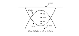
初期状態における上識別点電圧Vmと中央識別点電圧Vthと下識別点電圧Vsの各位置が、図6のようになっていると仮定する。すなわち、3点はアイ開口部内部にあるが、中央識別点電圧Vthは最適位置から若干上にずれている。
【0073】
この状態において、Hレベルエラー数CmとLレベルエラー数Csを計数すると、Cm<Cmin、Cs<Cminとなるので、ステップ401の一番目の判定がY(Yes)となり、アイ開口部の縁を検出するため、VmをΔVmだけ上にあげ、かつVsをΔVsだけ下に下げる(各識別点の幅を広げる)操作を行う(ステップ402)。この操作により、図7の状態になる。
【0074】
このとき、Hレベルエラー数Cm、Lレベルエラー数Csとも最小計測値Cminを下回っているので、計測時間内に計数するエラーパルスの数を増やして計測精度を上げるために計測時間TsampをΔTsampだけ長くする(ステップ403)。
【0075】
次に、図7において、上識別点電圧Vmと下識別点電圧Vsはアイ開口部の外側にずれているので、Hレベルエラー数CmとLレベルエラー数Csを計数すると、Cmax>Cm>Cs>Cminとなる。この結果、ステップ401の一番目の判定とステップ404の2番目の判定はN(No)となり、ステップ407の3番目の判定がY(Yes)となり、上識別点電圧Vmと中央識別点電圧Vthと下識別点電圧Vsを3点同時にΔVthだけだけ下げる制御を行うことにより(ステップ408)、図8の状態になる。
【0076】
このときも、Hレベルエラー数Cm、Lレベルエラー数Csは、最大計測値Cmaxを上回っていないので計測精度を上げるために計測時間TsampをΔTsampだけ長くする(ステップ409)。
【0077】
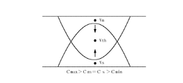
図8では、中央識別点電圧Vthは最適位置近傍あるが、まだ、上識別点電圧Vmと下識別点電圧Vsはアイ開口部の縁を検出しているとは言えない。このときのHレベルエラー数CmとLレベルエラー数Csの計数結果は、Cmax>Cm=Cs>Cminとなり、図5のフローチャートでは、ステップ401の一番目からステップ410の4番目の判定が全てN(No)となり、アイ開口部の縁を検出するため、上識別点電圧VmをΔVmだけ下げ、かつ下識別点電圧VsをΔVsだけ上げる(各識別点の幅を縮める)(ステップ413)。
【0078】
また同様に計測精度を上げるために計測時間TsampをΔTsampだけ長くする(ステップ414)。
【0079】
以上の操作を繰り返し行うことで、上識別点電圧Vmと下識別点電圧Vsでのエラー計測数が、Cmax>Cm=Cs≒Cminを満足する状態における中央識別点電圧Vthが最適識別点となる(図9)。
【0080】
図5において、Hレベルエラー数Cm、Lレベルエラー数Csのいずれかが最大計測値Cmaxを越えた場合は(ステップ404でYes)、上識別点電圧VmをΔVmだけ下げ、かつ下識別点電圧VsをΔVsだけ上げる(各識別点の幅を縮める)とともに(ステップ405)、計測時間TsampをΔTsampだけ短くする(ステップ406)。これにより、悪い状態からすばやく脱出することができ、またカウンタのオーバーフローを防ぐことができる。
【0081】
以上のような動作により、本実施の形態によれば、中央識別点電圧Vthが最適識別点となることで、図26に示すように、識別点固定の場合に比べてエラーレートの改善が図られるものである。
【0082】
図4における、識別点の制御とエラー計測時間の制御はそれぞれに単独で行ってもよいし、複数同時に行ってもよい。
【0083】
すなわち、上識別点電圧VmをΔVmだけ下げ、かつ下識別点電圧VsをΔVsだけ上げる(各識別点の幅を縮める)制御と、上識別点電圧Vmと中央識別点電圧Vthと下識別点Vsを3点同時にΔVthだけ下げる制御を同時に行ってもよい。
【0084】
例えば、図5においてHレベルエラー数Cm、Lレベルエラー数Csのいずれかが最大計測値Cmaxを越えた場合は、上識別点電圧VmをΔVmだけ下げ、かつ下識別点電圧VsをΔVsだけ上げる(各識別点の幅を縮める)とともに、計測時間TsampをΔTsampだけ短くする制御に加え、上識別点電圧Vmと中央識別点電圧Vthと下識別点電圧Vsを3点同時にΔVthだけ下げる制御を同時に行ったほうが、悪い状態からより早く脱出することができるであろう。
【0085】
また、計測結果において、Hレベルエラー数CmとLレベルエラー数Csが、Cmax>Cm>Cs>Cminを満たす場合は、計測数としては適切な値であるので、計測時間Tsampをかえないようにしてもよい。
【0086】
図5において一番目の判定と2番目の判定は逆の順番でもよい。同様に3番目と4番目の判定の順序が入れ替わってもよい。
【0087】
また、一番目の判定(ステップ401)、と3番目、4番目の判定(ステップ407、410)(又は4番目、3番目の判定)、2番目の判定(ステップ404)の順序で実行してもよい。あるいは、2番目の判定(ステップ404)、と3番目又は4番目の判定(ステップ407、410)(又は4番目、3番目の判定)、一番目の判定の順序で実行してもよい。
【0088】
また、ΔVmとΔVsは等しくてもよいし等しくなくてもよい。ΔVmとΔVsを等しい値に設定した場合は、中央識別点Vthは、上識別点電圧Vmと下識別点Vsの中間に位置することになる。
【0089】
上記説明において、ΔVm、ΔVs、ΔVthの値は、制御の精度をどの程度に設定するかによって変化することは言うまでもない。例えば、一般的な例では、入力データ信号の1/10〜1/1000の範囲で設定する。さらに、計測時間Tsamp及びΔTsampの値についても、制御の精度をどの程度に設定するかによって変化する。一例として、計測時間Tsampは、光受信装置が動作するエラーレートの最低値(例えば、BER=10−2〜10−3)を計測できる時間から、ほぼエラーフリーとみなされるエラーレート(例えば、BER=10−12〜10−15)を計測できる時間までの範囲で可変される。加えて、ΔTsampは、一例として、上述した時間的範囲のさらに1/10〜1/1000程度の刻みで設定する。
【0090】
次に、本発明の第2の実施の形態について説明する。図10は、本発明の第2の実施の形態による識別電圧制御回路の構成を示す図、図11は第2の実施の形態における制御アルゴリズムの基本的考え方を示す図、図12は、第2の実施の形態における制御アルゴリズムを用いたフローチャートの一例である。
【0091】
この、第2の実施の形態では、上述した第1の実施の形態をさらに簡略化したものであり、第1の実施の形態における上下各識別点電圧Vm、Vs及び中央識別点電圧Vthの間隔保持をしたままで3識別点を同時に動かす過程を省略した構成としている。その他の上下各識別点電圧Vm、Vsを移動するステップ及びエラー計測時間Tsampを変更するステップについては、図5の対応するステップと同じである。
【0092】
この第2の実施の形態による識別電圧制御回路10では、中央識別点電圧Vthは、演算処理部30により上下識別点Vm、Vsの間の任意に定められた点に設定される。アナログ電圧に変換後、分圧回路60を用いることにより、上下識別点電圧Vm、Vsの間の任意定められた点に設定する構成としている。
【0093】
次に、本発明の第3の実施の形態について説明する。図13は、本発明の第3の実施の形態による識別電圧制御回路の構成を示す図、図14は第3の実施の形態における制御アルゴリズムの基本的考え方を示す図、図15は、第3の実施の形態における制御アルゴリズムを用いたフローチャートの一例である。
【0094】
この第3の実施の形態では、第1の実施の形態による識別電圧制御回路10において、計測時間設定部40aに固定の計測時間が設定されており、エラーカウント部20における計数時間を固定し、エラー計測時間Tsampの変更を行わない構成としている。
【0095】
次に、本発明の第4の実施の形態について説明する。図16は、本発明の第4の実施の形態による識別電圧制御回路の構成を示す図、図17は第4の実施の形態における制御アルゴリズムの基本的考え方を示す図、図18は、第4の実施の形態における制御アルゴリズムを用いたフローチャートの一例である。
【0096】
この第4の実施の形態では、第2の実施の形態による識別電圧制御回路10の構成に加えて、エラーカウント部20における計数時間を固定し、エラー計測時間Tsampの変更を行わない構成としている。
【0097】
なお、第1から第4の実施の形態による識別電圧制御回路10における制御は、制御回路の各機能をハードウェア的に実現することは勿論として、各機能を備えるコンピュータプログラムである識別電圧制御プログラムを、コンピュータ処理装置のメモリにロードされることで実現することができる。この識別電圧制御プログラムは、磁気ディスク、半導体メモリその他の記録媒体600に格納される。そして、その記録媒体からコンピュータ処理装置にロードされ、コンピュータ処理装置の動作を制御することにより、上述した識別電圧制御回路10の各機能を実現する。
【0098】
上記の実施の形態では、識別電圧制御回路10をデジタル回路で実現した形態を説明したが、以下の第5から第7の実施の形態では、同様の機能を備える識別電圧制御回路をアナログ回路によって実現した形態を示す。
【0099】
まず、識別電圧制御回路をアナログ回路によって実現した第5の実施の形態について説明する。図20は、本発明の第5実施の形態による識別電圧制御回路の構成を示す図、図21は第5の実施の形態における制御アルゴリズムの基本的考え方を示す図である。この第5の実施の形態では、上識別点電圧Vm、下識別点電圧Vs、中央識別点電圧Vthの間隔が最適な位置になるようにアナログ的に制御するものである。
【0100】
この第5の実施の形態による識別電圧制御回路10Aは、HレベルエラーパルスとLレベルエラーパルスをそのレベルエラーの数に応じた直流電圧に変換するD/A変換部50Aと、演算部30Aとで構成される。また、演算部30Aは、演算増幅器301A、302Aとで構成され、D/A変換部50Aは、平均値検出回路501A〜503A及び論理和回路504Aとで構成される。
【0101】
以下、上記識別電圧制御回路10Aの動作について、図21を参照して説明する。D/A変換部50Aでは、平均値検出回路501AにおいてHレベルのエラーパルスの数に応じた直流電圧(Hレベルエラー電圧Cm)と、平均値検出回路502AにおいてLレベルのエラーパルスの数に応じた直流電圧(Lレベルエラー電圧Cs)と、HレベルとLレベルのエラーパルスの論理和のエラーパルスの数に応じた直流電圧(HLレベルエラー電圧C)とに変換して出力する。
【0102】
演算部30Aでは、演算増幅器301AがHレベルエラー電圧CmとLレベルエラー電圧Csの差電圧に比例する電圧を中央識別点電圧Vthとして与え、演算増幅器302AがHLレベルエラー電圧Cに逆比例した電圧を上識別点電圧Vmとして、HLレベルエラー電圧Cに比例した電圧を下識別点電圧Vsとして与える処理が行われる。これらの処理は同時に行われる。
【0103】
すなわち、上記において、Hレベルエラー数>Lレベルエラー数の場合、Hレベルエラー電圧Cm>Lレベルエラー電圧Csとなって中央識別点電圧Vthが下がると同時に、HLレベルエラー電圧Cも発生するので、上識別点電圧Vmが下がり、かつ下識別点電圧Vsが上がる。この結果、各識別点の間隔が狭くなる。
【0104】
また、各識別点の間隔制御において、間隔を広げる速度と狭める速度に差をつけたい場合には、HレベルとLレベルのエラーパルスの論理和のエラーパルスの数に応じた直流電圧に変換する過程において、充電時定数と放電時定数に差を設ければよい。
【0105】
上記の第5の実施の形態では、HレベルとLレベルのエラー数の計測結果に応じて、上識別点電圧Vm、下識別点電圧Vs及び中央識別点電圧Vthの3つの識別点の間隔が制御され、各識別点を最適な位置に調整することが可能となる。
【0106】
次に、識別電圧制御回路をアナログ回路によって実現した第6の実施の形態について説明する。図22は、本発明の第6の実施の形態による識別電圧制御回路の構成を示す図である。この第6の実施の形態では、上識別点電圧Vm、下識別点電圧Vs、中央識別点電圧Vthの間隔がを制御し、かつ各識別点の間隔を保持したまま3つの識別点を移動することにより、各識別点が最適な位置になるようにアナログ的に制御するものである。
【0107】
この第6の実施の形態による識別電圧制御回路10Bは、HレベルエラーパルスとLレベルエラーパルスをそのレベルエラーの数に応じた直流電圧に変換するD/A変換部50Bと、演算部30Bとで構成される。また、演算部30Bは、演算増幅器301B、302B、303Bとで構成され、D/A変換部50Aは、平均値検出回路501B〜503B及び論理和回路504Bとで構成される。ここで、演算部30B以外の構成は上記第5の実施の形態と同じである。
【0108】
演算部30Bでは、演算増幅器301BがHレベルエラー電圧CmとLレベルエラー電圧Csの差電圧に比例する電圧を中央識別点電圧Vthとして与え、演算増幅器302BがHLレベルエラー電圧Cと中央識別点電圧Vthの差電圧に比例した電圧を上識別点電圧Vmとして与え、演算増幅器303BがHLレベルエラー電圧Cと、Hレベルエラー電圧CmとLレベルエラー電圧Csの差電圧に逆比例する電圧との差電圧に比例した電圧を下識別点電圧Vsとして与える処理が行われる。
【0109】
上記ような構成により、中央識別点電圧Vthが上下に変化した場合には、上識別点電圧Vmと下識別点電圧Vsがそれに連動して上下に変化する。これにより、上記の第6の実施の形態では、HレベルとLレベルのエラー数の計測結果に応じて、上識別点電圧Vm、下識別点電圧Vs及び中央識別点電圧Vthの3つの識別点の間隔の制御がなされると共に、各識別点の間隔を保ちつつ3つの識別点を移動する制御がなされ、各識別点を最適な位置に調整することが可能となる。
【0110】
最後に、識別電圧制御回路をアナログ回路によって実現した第7の実施の形態について説明する。図23は、本発明の第7実施の形態による識別電圧制御回路の構成を示す図、図24は第7の実施の形態における制御アルゴリズムの基本的考え方を示す図である。この第7の実施の形態では、上識別点電圧Vm、下識別点電圧Vs、中央識別点電圧Vthの間隔が最適な位置になるようにアナログ的に制御するものである。
【0111】
この第7の実施の形態による識別電圧制御回路10Cは、HレベルエラーパルスとLレベルエラーパルスをそのレベルエラーの数に応じた直流電圧に変換するD/A変換部50Cと、演算部30Cとで構成される。また、演算部30Cは、演算増幅器301C、302Cと分圧器303Cとで構成され、D/A変換部50Aは、平均値検出回路501Cと502Cとで構成される。
【0112】
この識別電圧制御回路10Cでは、上識別点電圧Vmと下識別点電圧Vsの間隔制御のみを行い、中央点識別電圧Vthについては、上識別点電圧Vmと下識別点電圧Vsを分圧器303Cによって比例配分することで与えている。この分圧器303Cの分圧比にについては任意に設定することが可能である。
【0113】
上記第7の実施の形態によれば、Hレベルエラー電圧Cmが発生すると、上識別点電圧Vmが下がるように制御され、Lレベルエラー電圧Csが発生すると下識別点電圧Vsが上がるように制御される。これにより、上識別点電圧Vm、下識別点電圧Vs、中央識別点電圧Vthの間隔が最適な位置になるように制御される。
【0114】
なお、上記第5から第7の実施の形態においても、第1の実施の形態と同様に、Hレベルエラー電圧CmとLレベルエラー電圧Csの大きさによって、計測時間を設定するような構成とすることも可能である。
【0115】
以上好ましい実施の形態及び実施例をあげて本発明を説明したが、本発明は必ずしも上記実施の形態及び実施例に限定されるものではなく、その技術的思想の範囲内において様々に変形して実施することができる。
【0116】
【発明の効果】
以上説明したように本発明の識別電圧付与機能付きCDRの識別電圧制御回路と識別電圧制御方法によれば、以下のような効果が達成される。
【0117】
第1に、各受光レベルで識別位置を最適に制御することができるので、識別点が固定されていた従来の識別回路に比べてエラーレート特性が改善され、フロアーを生じることがなくなる。
【0118】
第2に、アイ開口部の内縁を検出するので識別点Vthを最適位置に制御することができる。
【0119】
第3に、エラーカウント部の計測結果をもとに、計測時間を調整しているので、計測精度を上げることができ、また、悪い状態からすばやく脱出することができる。
【0120】
第4に、計測したエラーの数に応じて、計測時間を変更するので、いたずらに大規模なカウンタを用いる必要がない。
【図面の簡単な説明】
【図1】 本発明の第1の実施の形態による識別電圧付加機能付きCDRの識別電圧制御回路の構成を示すブロック図である。
【図2】 本発明の第1の実施の形態における識別電圧付加機能付きCDRの構成を示すブロック図である。
【図3】 本発明の本発明による識別電圧制御回路を適用した光受信装置の構成を示すブロック図である。
【図4】 本発明の第1の実施の形態による識別電圧制御回路の演算処理部における制御アルゴリズムの基本的考え方を示す図である。
【図5】 本発明の第1の実施の形態による識別電圧制御回路の動作を説明するフローチャートである。
【図6】 図5のフローチャート各過程におけるアイ開口部と上識別点電圧と中央識別点と下識別点Vとの位置関係を示す図である。
【図7】 図5のフローチャート各過程におけるアイ開口部と上識別点電圧と中央識別点と下識別点Vとの位置関係を示す図である。
【図8】 図5のフローチャート各過程におけるアイ開口部と上識別点電圧と中央識別点と下識別点Vとの位置関係を示す図である。
【図9】 図5のフローチャート各過程におけるアイ開口部と上識別点電圧と中央識別点と下識別点Vとの位置関係を示す図である。
【図10】 本発明の第2の実施の形態による識別電圧付加機能付きCDRの識別電圧制御回路の構成を示すブロック図である。
【図11】 本発明の第2の実施の形態による識別電圧制御回路の演算処理部における制御アルゴリズムの基本的考え方を示す図である。
【図12】 本発明の第2の実施の形態による識別電圧制御回路の動作を説明するフローチャートである。
【図13】 本発明の第3の実施の形態による識別電圧付加機能付きCDRの識別電圧制御回路の構成を示すブロック図である。
【図14】 本発明の第3の実施の形態による識別電圧制御回路の演算処理部における制御アルゴリズムの基本的考え方を示す図である。
【図15】 本発明の第3の実施の形態による識別電圧制御回路の動作を説明するフローチャートである。
【図16】 本発明の第4の実施の形態による識別電圧付加機能付きCDRの識別電圧制御回路の構成を示すブロック図である。
【図17】 本発明の第4の実施の形態による識別電圧制御回路の演算処理部における制御アルゴリズムの基本的考え方を示す図である。
【図18】 本発明の第4の実施の形態による識別電圧制御回路の動作を説明するフローチャートである。
【図19】 送信後の光受信波形の例を示す図である。
【図20】 本発明の第5実施の形態によるアナログ的な識別電圧制御回路の構成を示すブロック図である。
【図21】 第5の実施の形態における制御アルゴリズムの基本的考え方を示す図である。
【図22】 本発明の第6の実施の形態によるアナログ的な識別電圧制御回路の構成を示すブロック図である。
【図23】 本発明の第7の実施の形態によるアナログ的な識別電圧制御回路の構成を示すブロック図である。
【図24】 第7の実施の形態における制御アルゴリズムの基本的考え方を示す図である。
【図25】 送信後の光受信波形の例を示す図である。
【図26】 エラーレートの改善効果を示す図である。
【符号の説明】
10、10A、10B、10C 識別電圧制御回路
20 エラーカウント部
30 演算処理部
40 計測時間設定部
50、50A、50B、50C D/A変換部
100 識別電圧付加機能付きCDR
200 光受信装置
210 光/電気変換回路
30A、30B、30C 演算部
301A、302A、301B、302B、303B、301C、302C 演算増幅器
501A、502A、503A、501B、502B、503B、501C、502C 平均値検出回路
504A、504B 論理和回路
303C 分圧器[0001]
BACKGROUND OF THE INVENTION
The present invention relates to a control circuit, an identification voltage control method, and an identification voltage control program for providing an optimum identification voltage to a clock data recovery circuit in a clock data recovery circuit with an identification voltage application function.
[0002]
[Prior art]
In recent optical transmission systems including optical amplifiers and WDM (wavelength multiplex transmission), there are an increasing number of factors that degrade optical reception waveforms as compared to conventional optical transmission systems. Examples include accumulation of noise caused by ASE (amplified spontaneous emission) generated by optical fiber amplifiers, waveform degradation due to dispersion of optical fibers and nonlinear effects, the effect of which became significant due to the increase in optical signal power in the optical fiber, Crosstalk and the like from adjacent channels in wavelength multiplex transmission are raised.
[0003]
As shown in FIG. 19, the optical reception waveform immediately after transmission is a region where the optical input data signal can be reliably identified as 1 or 0 and the eye opening is large, but the optical reception waveform after 600 km transmission is shown in FIG. As such, the eye opening is very small.
[0004]
Even if there is such degradation of the optical reception waveform, the identification circuit of the reception circuit is required to perform optimum identification. Since the eye opening portion of the optical reception waveform varies depending on the received light power, the optimum value of the identification position for identifying 1 or 0 of the optical reception waveform varies depending on the received light power. There is a relatively large margin for the identification position against the waveform deterioration, and even if it is fixed to a value adjusted by the manufacturer at the time of product shipment, there is no practical problem.
[0005]
[Problems to be solved by the invention]
However, in an optical transmission system including an optical amplifier and WDM (wavelength multiplex transmission), as described above, the factors that deteriorate the optical reception waveform have increased. Therefore, in the conventional identification circuit in which the identification position is fixed, error rate characteristics Therefore, it becomes difficult to ensure the quality of the transmission path (upper side in FIG. 26).
[0006]
In view of such a situation, various identification circuits that optimally control the identification position in hardware have been considered. However, since arithmetic processing is performed, it is necessary to design circuit parameters precisely and not much. There was a disadvantage that fine control was impossible.
[0007]
In order to overcome such drawbacks, the object of the present invention is to optimally control the identification position at each light receiving level by using digital arithmetic processing in the identification voltage control circuit, and the identification point is fixed. An object of the present invention is to propose an identification voltage control circuit and an identification voltage control method for a clock data recovery circuit with an identification voltage application function, which has improved error rate characteristics compared to conventional identification circuits and eliminates the occurrence of a floor.
[0008]
A second object of the present invention is to provide an identification voltage control circuit and an identification voltage control for a clock data reproduction circuit with an identification voltage applying function capable of controlling the central identification point to an optimum position by detecting the inner edge of the eye opening. To propose a method.
[0009]
The third object of the present invention is to adjust the measurement time based on the measurement result of the error count unit, so that the measurement accuracy can be improved and the identification voltage can be quickly escaped from a bad state. An object is to propose an identification voltage control circuit and an identification voltage control method for a clock data recovery circuit with a function.
[0010]
The fourth object of the present invention is to change the measurement time according to the number of measured errors, so that it is not necessary to use a large-scale counter unnecessarily. And to propose an identification voltage control method.
[0013]
[0014]
[0015]
[0016]
[0019]
[0020]
Claim 6 The present invention relates to a clock data recovery circuit for converting a light input signal into an electric signal, extracting a clock component from the input data signal amplified to a predetermined amplitude, and identifying 1 or 0 of the input data signal at the timing of the clock In addition, in the identification voltage control circuit for applying an optimum identification voltage, an error count unit for counting the number of errors near the H level and the number of errors near the L level of the input data signal, and the H count based on the error count result, An arithmetic processing unit that changes the width of the upper discrimination point near the level and the central discrimination point or the lower discrimination point near the L level, and changes the measurement time of the number of errors based on the error count result, The center identification point is set to an optimum position while detecting the inner edge of the eye opening of the input data signal.
[0021]
Claim 7 The present invention relates to a clock data recovery circuit for converting a light input signal into an electric signal, extracting a clock component from the input data signal amplified to a predetermined amplitude, and identifying 1 or 0 of the input data signal at the timing of the clock In addition, in the identification voltage control circuit for applying an optimum identification voltage, an error count unit for counting the number of errors near the H level and the number of errors near the L level of the input data signal, and the H count based on the error count result, The width of the upper discrimination point near the level and the central discrimination point or the lower discrimination point near the L level is changed, and the interval between the upper and lower discrimination points and the central discrimination point is kept based on the error count result. And an arithmetic processing unit for simultaneously moving the three identification points, wherein the central identification point is set to an optimum position while detecting an inner edge of the eye opening of the input data signal. .
[0022]
Claim 8 The present invention relates to a clock data recovery circuit for converting a light input signal into an electric signal, extracting a clock component from the input data signal amplified to a predetermined amplitude, and identifying 1 or 0 of the input data signal at the timing of the clock In addition, in the identification voltage control circuit for applying an optimum identification voltage, an error count unit for counting the number of errors near the H level and the number of errors near the L level of the input data signal, and the H count based on the error count result, An arithmetic processing unit that changes the width of the upper discrimination point near the level and the central discrimination point or the lower discrimination point near the L level, and detects the inner discrimination point while detecting the inner edge of the eye opening of the input data signal. The optimal position is set.
[0025]
Claim 9 The present invention relates to a clock data recovery circuit for converting a light input signal into an electric signal, extracting a clock component from the input data signal amplified to a predetermined amplitude, and identifying 1 or 0 of the input data signal at the timing of the clock An error count unit for counting and processing the number of errors near the H level and the number of errors near the L level of the input data signal in the clock data recovery circuit with an identification voltage addition function to which a function for applying an identification voltage is added. Based on the error count result, the width between the upper discrimination point near the H level and the central discrimination point or the lower discrimination point near the L level is changed, and based on the error count result, the upper and lower discrimination points and An arithmetic processing unit that moves the three identification points at the same time while maintaining the interval between the central identification points, and changes the measurement time of the number of errors based on the error count result; Provided, characterized by comprising an identification voltage control circuit for setting the optimum position of the center decision point while detecting the inner edge of the eye opening of the input data signal.
[0026]
[0027]
[0028]
[0031]
[0032]
[0033]
Claim 15 The present invention is read and executed by a computer device, and controls the computer device to convert a light input signal into an electric signal and extract a clock component from an input data signal amplified to a predetermined amplitude. In the identification voltage control program for assigning an optimum identification voltage to the clock data recovery circuit that identifies 1 or 0 of the input data signal at the timing, the number of errors near the H level and the number of errors near the L level of the input data signal are calculated. Counting is performed, and based on the error count result, the width of the upper discrimination point near the H level and the central discrimination point or the lower discrimination point near the L level is changed. Detecting the inner edge of the eye opening of the input data signal including the step of simultaneously moving the three identification points while maintaining the distance between the identification point and the central identification point Characterized in that to realize the function of setting the central decision point to the optimum position while.
[0034]
Claim 16 The present invention is read and executed by a computer device, and controls the computer device to convert a light input signal into an electric signal and extract a clock component from an input data signal amplified to a predetermined amplitude. In the identification voltage control program for assigning an optimum identification voltage to the clock data recovery circuit that identifies 1 or 0 of the input data signal at the timing, the number of errors near the H level and the number of errors near the L level of the input data signal are calculated. An eye opening portion of the input data signal including a step of changing the width between the upper discrimination point near the H level and the central discrimination point or the lower discrimination point near the L level based on the error count result. It is characterized in that a function for setting the central discrimination point to the optimum position while detecting the inner edge of the image is realized.
[0037]
Claim 17 According to the present invention, an optical / electrical conversion circuit that converts an optical input signal into an electrical signal and outputs it as an input data signal, and extracts a clock component from the input data signal amplified to a predetermined amplitude, and at the timing of the clock In an optical receiving apparatus including a clock data recovery circuit for identifying 1 or 0 of an input data signal, the clock data recovery circuit having an identification voltage adding function to which a function of applying an identification voltage is added, an H of the input data signal An error count unit for counting the number of errors in the vicinity of the level and the number of errors in the vicinity of the L level, and based on the error count result, an upper discrimination point near the H level and a central discrimination point, or a lower discrimination point near the L level The three discrimination points are moved at the same time while maintaining the distance between the upper and lower discrimination points and the center discrimination point based on the error count result. An identification voltage control circuit for setting a central identification point at an optimum position while detecting an inner edge of an eye opening of the input data signal, and an arithmetic processing unit that changes a measurement time of the number of errors based on an error count result It is characterized by having.
[0038]
Claim 18 According to the present invention, an optical / electrical conversion circuit that converts an optical input signal into an electrical signal and outputs it as an input data signal, and extracts a clock component from the input data signal amplified to a predetermined amplitude, and at the timing of the clock In an optical receiving apparatus including a clock data recovery circuit for identifying 1 or 0 of an input data signal, the clock data recovery circuit having an identification voltage adding function to which a function of applying an identification voltage is added, an H of the input data signal An error count unit for counting the number of errors in the vicinity of the level and the number of errors in the vicinity of the L level, and based on the error count result, an upper discrimination point near the H level and a central discrimination point, or a lower discrimination point near the L level An arithmetic processing unit that changes a measurement time of the number of errors based on the error count result, and an eye opening of the input data signal Characterized by comprising an identification voltage control circuit for setting the central decision point to the optimum position while detecting the inner edge.
[0039]
Claim 19 According to the present invention, an optical / electrical conversion circuit that converts an optical input signal into an electrical signal and outputs it as an input data signal, and extracts a clock component from the input data signal amplified to a predetermined amplitude, and at the timing of the clock In an optical receiving apparatus including a clock data recovery circuit for identifying 1 or 0 of an input data signal, the clock data recovery circuit having an identification voltage adding function to which a function of applying an identification voltage is added, an H of the input data signal An error count unit for counting the number of errors in the vicinity of the level and the number of errors in the vicinity of the L level, and based on the error count result, an upper discrimination point near the H level and a central discrimination point, or a lower discrimination point near the L level Based on the error count result, the distance between the upper and lower discrimination points and the center discrimination point is maintained, and the three discrimination points are moved simultaneously. And a processing unit, characterized by comprising an identification voltage control circuit for setting the optimum position of the center decision point while detecting the inner edge of the eye opening of the input data signal.
[0040]
[0041]
[0042]
[0043]
Claim 23 In the identification voltage control circuit of the present invention, the arithmetic unit divides a voltage corresponding to the upper identification point near the H level and a voltage corresponding to the lower identification point near the L level by an arbitrary voltage dividing ratio, and A voltage divider that outputs a voltage corresponding to the discrimination point is provided.
[0044]
[0055]
DETAILED DESCRIPTION OF THE INVENTION
Hereinafter, embodiments of the present invention will be described in detail with reference to the drawings.
[0056]
FIG. 1 is a block diagram showing a configuration of an identification voltage control circuit of a CDR with an identification voltage adding function according to the first embodiment of the present invention.
[0057]
In FIG. 1,
[0058]
The
[0059]
The identification
[0060]
The
[0061]
The
(1) A process of changing the width of the discrimination point near the H level (upper discrimination point) and the central discrimination point or the discrimination point (lower discrimination point) near the L level
(2) The process of moving the three discrimination points simultaneously while maintaining the intervals between the upper and lower discrimination points and the central discrimination point
(3) One or a plurality of processes for changing the counting time are executed according to the number of errors counted.
[0062]
The measurement
[0063]
The D /
[0064]
In the above configuration, the identification voltage control circuit has been described as a separate circuit from the
[0065]
With reference to FIG. 2, the configuration of the
[0066]
In FIG. 2, a
[0067]
Here, the
[0068]
FIG. 3 shows a configuration of an optical receiver to which the identification
[0069]
The operation of the identification voltage control circuit according to the embodiment of the present invention will be described with reference to FIGS.
[0070]
FIG. 4 is a diagram showing a basic concept of a control algorithm in the
[0071]
here,
Number of H level errors: Cm
Number of L level errors: Cs
Maximum measured value: Cmax (Cmax>Cmin> 0)
Minimum measured value: Cmin (Cmin> = 0)
H level identification point voltage: Vm
L level identification point voltage: Vs
Central identification point voltage: Vth (Vm>Vth> Vs)
Error measurement time: Tsamp
It is defined as
[0072]
Assume that the positions of the upper discrimination point voltage Vm, the central discrimination point voltage Vth, and the lower discrimination point voltage Vs in the initial state are as shown in FIG. That is, although the three points are inside the eye opening, the central discrimination point voltage Vth is slightly shifted from the optimum position.
[0073]
In this state, when the number of H level errors Cm and the number of L level errors Cs are counted, Cm <Cmin and Cs <Cmin are satisfied. Therefore, the first determination in
[0074]
At this time, since the number of H level errors Cm and the number of L level errors Cs are below the minimum measurement value Cmin, the measurement time Tsamp is set to ΔTsamp in order to increase the number of error pulses counted within the measurement time and increase the measurement accuracy. Increase the length (step 403).
[0075]
Next, in FIG. 7, since the upper discrimination point voltage Vm and the lower discrimination point voltage Vs are shifted to the outside of the eye opening, when the H level error number Cm and the L level error number Cs are counted, Cmax>Cm> Cs > Cmin. As a result, the first determination in
[0076]
Also at this time, since the number of H level errors Cm and the number of L level errors Cs do not exceed the maximum measured value Cmax, the measurement time Tsamp is increased by ΔTsamp in order to increase the measurement accuracy (step 409).
[0077]
In FIG. 8, the center discrimination point voltage Vth is in the vicinity of the optimal position, but it cannot be said that the upper discrimination point voltage Vm and the lower discrimination point voltage Vs have detected the edge of the eye opening. The counting results of the H level error number Cm and the L level error number Cs at this time are Cmax> Cm = Cs> Cmin. In the flowchart of FIG. In order to detect the edge of the eye opening, the upper discrimination point voltage Vm is lowered by ΔVm and the lower discrimination point voltage Vs is raised by ΔVs (the width of each discrimination point is reduced) (step 413).
[0078]
Similarly, in order to increase the measurement accuracy, the measurement time Tsamp is lengthened by ΔTsamp (step 414).
[0079]
By repeating the above operation, the central discrimination point voltage Vth in the state where the number of error measurements at the upper discrimination point voltage Vm and the lower discrimination point voltage Vs satisfies Cmax> Cm = Cs≈Cmin becomes the optimum discrimination point. (FIG. 9).
[0080]
In FIG. 5, when either the H level error number Cm or the L level error number Cs exceeds the maximum measured value Cmax (Yes in Step 404), the upper discrimination point voltage Vm is lowered by ΔVm and the lower discrimination point voltage is set. Vs is increased by ΔVs (the width of each identification point is reduced) (step 405), and the measurement time Tsamp is shortened by ΔTsamp (step 406). Thereby, it is possible to quickly escape from a bad state and to prevent the counter from overflowing.
[0081]
Through the operation as described above, according to the present embodiment, since the central discrimination point voltage Vth becomes the optimum discrimination point, the error rate can be improved as compared with the case where the discrimination point is fixed as shown in FIG. It is what
[0082]
In FIG. 4, the control of the identification points and the control of the error measurement time may be performed individually or in combination.
[0083]
That is, control for lowering the upper discrimination point voltage Vm by ΔVm and raising the lower discrimination point voltage Vs by ΔVs (reducing the width of each discrimination point), upper discrimination point voltage Vm, central discrimination point voltage Vth, and lower discrimination point Vs It is also possible to simultaneously perform control for lowering three points by ΔVth.
[0084]
For example, in FIG. 5, when either the H level error count Cm or the L level error count Cs exceeds the maximum measured value Cmax, the upper discrimination point voltage Vm is lowered by ΔVm and the lower discrimination point voltage Vs is increased by ΔVs. In addition to the control for shortening the measurement time Tsamp by ΔTsamp (at the same time reducing the width of each discrimination point), the control for simultaneously reducing the upper discrimination point voltage Vm, the central discrimination point voltage Vth, and the lower discrimination point voltage Vs by ΔVth simultaneously. If you do, you will be able to escape earlier from the bad.
[0085]
In the measurement result, when the number of H level errors Cm and the number of L level errors Cs satisfy Cmax>Cm>Cs> Cmin, the measurement number is an appropriate value, so that the measurement time Tsamp is not changed. May be.
[0086]
In FIG. 5, the first determination and the second determination may be reversed. Similarly, the order of the third and fourth determinations may be switched.
[0087]
Also, the first determination (step 401), the third determination, the fourth determination (
[0088]
Further, ΔVm and ΔVs may or may not be equal. When ΔVm and ΔVs are set to the same value, the center discrimination point Vth is positioned between the upper discrimination point voltage Vm and the lower discrimination point Vs.
[0089]
In the above description, it goes without saying that the values of ΔVm, ΔVs, and ΔVth vary depending on how much control accuracy is set. For example, in a general example, it is set in the range of 1/10 to 1/1000 of the input data signal. Furthermore, the values of the measurement times Tsamp and ΔTsamp also vary depending on how much control accuracy is set. As an example, the measurement time Tsamp is the lowest error rate (for example, BER = 10) at which the optical receiver operates. -2 -10 -3 ) Can be measured from an error rate (for example, BER = 10) that is considered almost error-free. -12 -10 -15 ) Is variable in the range up to the time that can be measured. In addition, ΔTsamp is set, for example, in steps of about 1/10 to 1/1000 of the time range described above.
[0090]
Next, a second embodiment of the present invention will be described. FIG. 10 is a diagram showing the configuration of the identification voltage control circuit according to the second embodiment of the present invention, FIG. 11 is a diagram showing the basic concept of the control algorithm in the second embodiment, and FIG. It is an example of the flowchart using the control algorithm in the embodiment.
[0091]
In the second embodiment, the first embodiment described above is further simplified, and the intervals between the upper and lower discrimination point voltages Vm and Vs and the central discrimination point voltage Vth in the first embodiment. The process of moving the three identification points simultaneously while maintaining the configuration is omitted. The other steps of moving the upper and lower discrimination point voltages Vm and Vs and the step of changing the error measurement time Tsamp are the same as the corresponding steps in FIG.
[0092]
In the discrimination
[0093]
Next, a third embodiment of the present invention will be described. FIG. 13 is a diagram showing a configuration of an identification voltage control circuit according to the third embodiment of the present invention, FIG. 14 is a diagram showing a basic concept of a control algorithm in the third embodiment, and FIG. It is an example of the flowchart using the control algorithm in the embodiment.
[0094]
In the third embodiment, in the identification
[0095]
Next, a fourth embodiment of the present invention will be described. FIG. 16 is a diagram showing a configuration of an identification voltage control circuit according to the fourth embodiment of the present invention, FIG. 17 is a diagram showing a basic concept of a control algorithm in the fourth embodiment, and FIG. It is an example of the flowchart using the control algorithm in the embodiment.
[0096]
In the fourth embodiment, in addition to the configuration of the identification
[0097]
The identification
[0098]
In the above embodiment, the identification
[0099]
First, a fifth embodiment in which the identification voltage control circuit is realized by an analog circuit will be described. FIG. 20 is a diagram showing a configuration of an identification voltage control circuit according to the fifth embodiment of the present invention, and FIG. 21 is a diagram showing a basic concept of a control algorithm in the fifth embodiment. In the fifth embodiment, the control is performed in an analog manner so that the intervals of the upper discrimination point voltage Vm, the lower discrimination point voltage Vs, and the central discrimination point voltage Vth are optimal positions.
[0100]
The identification
[0101]
Hereinafter, the operation of the identification
[0102]
In the
[0103]
That is, in the above, when the number of H level errors> the number of L level errors, the H level error voltage Cm> L level error voltage Cs and the central discrimination point voltage Vth decreases, and at the same time, the HL level error voltage C is generated. The upper discrimination point voltage Vm decreases and the lower discrimination point voltage Vs increases. As a result, the interval between the identification points is narrowed.
[0104]
In addition, in the interval control of each discrimination point, when it is desired to make a difference between the speed of expanding the interval and the speed of narrowing, it is converted into a DC voltage corresponding to the number of error pulses of the logical sum of the H level and L level error pulses. In the process, a difference may be provided between the charge time constant and the discharge time constant.
[0105]
In the fifth embodiment, the intervals between the three identification points, that is, the upper identification point voltage Vm, the lower identification point voltage Vs, and the central identification point voltage Vth are determined according to the measurement results of the number of errors at the H level and the L level. Controlled, each discrimination point can be adjusted to an optimum position.
[0106]
Next, a sixth embodiment in which the identification voltage control circuit is realized by an analog circuit will be described. FIG. 22 is a diagram showing a configuration of an identification voltage control circuit according to the sixth embodiment of the present invention. In the sixth embodiment, the intervals of the upper discrimination point voltage Vm, the lower discrimination point voltage Vs, and the central discrimination point voltage Vth are controlled, and three discrimination points are moved while maintaining the intervals of the discrimination points. Thus, the control is performed in an analog manner so that each discrimination point is in an optimum position.
[0107]
The identification
[0108]
In the
[0109]
With the above configuration, when the central discrimination point voltage Vth changes up and down, the upper discrimination point voltage Vm and the lower discrimination point voltage Vs change up and down in conjunction with it. As a result, in the sixth embodiment, the three discrimination points of the upper discrimination point voltage Vm, the lower discrimination point voltage Vs, and the central discrimination point voltage Vth according to the measurement results of the number of errors at the H level and the L level. And the control of moving the three identification points while maintaining the interval between the respective identification points, so that each identification point can be adjusted to an optimum position.
[0110]
Finally, a seventh embodiment in which the identification voltage control circuit is realized by an analog circuit will be described. FIG. 23 is a diagram showing a configuration of an identification voltage control circuit according to the seventh embodiment of the present invention, and FIG. 24 is a diagram showing a basic concept of a control algorithm in the seventh embodiment. In the seventh embodiment, the control is performed in an analog manner so that the intervals of the upper discrimination point voltage Vm, the lower discrimination point voltage Vs, and the center discrimination point voltage Vth are optimal positions.
[0111]
The identification
[0112]
In this discrimination
[0113]
According to the seventh embodiment, when the H level error voltage Cm is generated, the upper identification point voltage Vm is controlled to decrease, and when the L level error voltage Cs is generated, the lower identification point voltage Vs is controlled to increase. Is done. As a result, control is performed so that the intervals of the upper discrimination point voltage Vm, the lower discrimination point voltage Vs, and the central discrimination point voltage Vth are optimal positions.
[0114]
In the fifth to seventh embodiments, as in the first embodiment, the measurement time is set according to the magnitudes of the H level error voltage Cm and the L level error voltage Cs. It is also possible to do.
[0115]
Although the present invention has been described with reference to the preferred embodiments and examples, the present invention is not necessarily limited to the above-described embodiments and examples, and various modifications can be made within the scope of the technical idea. Can be implemented.
[0116]
【The invention's effect】
As described above, according to the identification voltage control circuit and the identification voltage control method of the CDR with the identification voltage application function of the present invention, the following effects are achieved.
[0117]
First, since the identification position can be optimally controlled at each light receiving level, the error rate characteristic is improved as compared with the conventional identification circuit in which the identification point is fixed, and a floor is not generated.
[0118]
Second, since the inner edge of the eye opening is detected, the discrimination point Vth can be controlled to the optimum position.
[0119]
Thirdly, since the measurement time is adjusted based on the measurement result of the error count unit, the measurement accuracy can be increased, and the user can quickly escape from a bad state.
[0120]
Fourth, since the measurement time is changed according to the number of measured errors, it is not necessary to use a large-scale counter.
[Brief description of the drawings]
FIG. 1 is a block diagram showing a configuration of an identification voltage control circuit of a CDR with an identification voltage adding function according to a first embodiment of the present invention.
FIG. 2 is a block diagram showing a configuration of a CDR with an identification voltage addition function according to the first embodiment of the present invention.
FIG. 3 is a block diagram showing a configuration of an optical receiving apparatus to which an identification voltage control circuit according to the present invention is applied.
FIG. 4 is a diagram showing a basic concept of a control algorithm in an arithmetic processing unit of the identification voltage control circuit according to the first embodiment of the present invention.
FIG. 5 is a flowchart for explaining the operation of the identification voltage control circuit according to the first embodiment of the present invention;
6 is a diagram showing a positional relationship among an eye opening, an upper discrimination point voltage, a center discrimination point, and a lower discrimination point V in each process of the flowchart of FIG. 5;
7 is a diagram showing a positional relationship among an eye opening, an upper discrimination point voltage, a center discrimination point, and a lower discrimination point V in each process of the flowchart of FIG. 5;
8 is a diagram showing a positional relationship among an eye opening, an upper discrimination point voltage, a center discrimination point, and a lower discrimination point V in each process of the flowchart of FIG.
9 is a diagram showing a positional relationship among an eye opening, an upper discrimination point voltage, a center discrimination point, and a lower discrimination point V in each process of the flowchart of FIG.
FIG. 10 is a block diagram showing a configuration of an identification voltage control circuit of a CDR with an identification voltage addition function according to a second embodiment of the present invention.
FIG. 11 is a diagram showing a basic concept of a control algorithm in an arithmetic processing unit of an identification voltage control circuit according to a second embodiment of the present invention.
FIG. 12 is a flowchart for explaining the operation of the identification voltage control circuit according to the second embodiment of the present invention;
FIG. 13 is a block diagram showing a configuration of an identification voltage control circuit of a CDR with an identification voltage adding function according to a third embodiment of the present invention.
FIG. 14 is a diagram showing a basic concept of a control algorithm in an arithmetic processing unit of an identification voltage control circuit according to a third embodiment of the present invention.
FIG. 15 is a flowchart for explaining the operation of the identification voltage control circuit according to the third embodiment of the present invention;
FIG. 16 is a block diagram showing a configuration of an identification voltage control circuit of a CDR with an identification voltage adding function according to a fourth embodiment of the present invention.
FIG. 17 is a diagram illustrating a basic concept of a control algorithm in an arithmetic processing unit of an identification voltage control circuit according to a fourth embodiment of the present invention.
FIG. 18 is a flowchart for explaining the operation of the identification voltage control circuit according to the fourth embodiment of the present invention;
FIG. 19 is a diagram illustrating an example of an optical reception waveform after transmission.
FIG. 20 is a block diagram showing a configuration of an analog identification voltage control circuit according to a fifth embodiment of the present invention.
FIG. 21 is a diagram showing a basic concept of a control algorithm in the fifth embodiment.
FIG. 22 is a block diagram showing a configuration of an analog identification voltage control circuit according to a sixth embodiment of the present invention.
FIG. 23 is a block diagram showing a configuration of an analog identification voltage control circuit according to a seventh embodiment of the present invention.
FIG. 24 is a diagram showing a basic concept of a control algorithm in the seventh embodiment.
FIG. 25 is a diagram illustrating an example of an optical reception waveform after transmission.
FIG. 26 is a diagram illustrating an effect of improving an error rate.
[Explanation of symbols]
10, 10A, 10B, 10C Identification voltage control circuit
20 Error count section
30 arithmetic processing unit
40 Measurement time setting section
50, 50A, 50B, 50C D / A converter
100 CDR with identification voltage addition function
200 Optical receiver
210 Optical / electrical conversion circuit
30A, 30B, 30C arithmetic unit
301A, 302A, 301B, 302B, 303B, 301C, 302C operational amplifier
501A, 502A, 503A, 501B, 502B, 503B, 501C, 502C Average value detection circuit
504A, 504B OR circuit
303C voltage divider
Claims (24)
入力データ信号のHレベル近傍のエラー数とLレベル近傍のエラー数を計数処理し、
前記エラー計数結果に基づいて、Hレベル近傍の上識別点と中央識別点又は、Lレベル近傍の下識別点との幅を変化させ、
前記エラー計数結果に基づいて、前記上下各識別点及び中央識別点の間隔保持をしたままで、3識別点を同時に動かす過程
前記エラー計数結果に基づいて、エラー数の計測時間を変化させる過程とを含み、
前記入力データ信号のアイ開口部の内縁を検出しながら中央識別点を最適位置に設定することを特徴とする識別電圧制御方法。Optimal identification for a clock data recovery circuit that converts an optical input signal into an electrical signal, extracts a clock component from the input data signal amplified to a predetermined amplitude, and identifies 1 or 0 of the input data signal at the timing of the clock In an identification voltage control method for applying a voltage,
Count the number of errors near the H level of the input data signal and the number of errors near the L level,
Based on the error count result, the width of the upper discrimination point near the H level and the central discrimination point or the lower discrimination point near the L level is changed,
Based on the error count result, the process of simultaneously moving the three discrimination points while maintaining the interval between the upper and lower discrimination points and the central discrimination point, and the process of changing the error count measurement time based on the error count result; Including
A discrimination voltage control method, wherein a central discrimination point is set at an optimum position while detecting an inner edge of an eye opening of the input data signal.
入力データ信号のHレベル近傍のエラー数とLレベル近傍のエラー数を計数処理し、
前記エラー計数結果に基づいて、Hレベル近傍の上識別点と中央識別点又は、Lレベル近傍の下識別点との幅を変化させ、
前記エラー計数結果に基づいて、エラー数の計測時間を変化させる過程とを含み、
前記入力データ信号のアイ開口部の内縁を検出しながら中央識別点を最適位置に設定することを特徴とする識別電圧制御方法。Optimal identification for a clock data recovery circuit that converts an optical input signal into an electrical signal, extracts a clock component from the input data signal amplified to a predetermined amplitude, and identifies 1 or 0 of the input data signal at the timing of the clock In an identification voltage control method for applying a voltage,
Count the number of errors near the H level of the input data signal and the number of errors near the L level,
Based on the error count result, the width of the upper discrimination point near the H level and the central discrimination point or the lower discrimination point near the L level is changed,
Changing the measurement time of the number of errors based on the error count result,
A discrimination voltage control method, wherein a central discrimination point is set at an optimum position while detecting an inner edge of an eye opening of the input data signal.
入力データ信号のHレベル近傍のエラー数とLレベル近傍のエラー数を計数処理し、
前記エラー計数結果に基づいて、Hレベル近傍の上識別点と中央識別点又は、Lレベル近傍の下識別点との幅を変化させ、
前記エラー計数結果に基づいて、前記上下各識別点及び中央識別点の間隔保持をしたままで、3識別点を同時に動かす過程とを含み、
前記入力データ信号のアイ開口部の内縁を検出しながら中央識別点を最適位置に設定することを特徴とする識別電圧制御方法。Optimal identification for a clock data recovery circuit that converts an optical input signal into an electrical signal, extracts a clock component from the input data signal amplified to a predetermined amplitude, and identifies 1 or 0 of the input data signal at the timing of the clock In an identification voltage control method for applying a voltage,
Count the number of errors near the H level of the input data signal and the number of errors near the L level,
Based on the error count result, the width of the upper discrimination point near the H level and the central discrimination point or the lower discrimination point near the L level is changed,
Based on the error count result, and simultaneously moving the three discrimination points while maintaining the interval between the upper and lower discrimination points and the central discrimination point,
A discrimination voltage control method, wherein a central discrimination point is set at an optimum position while detecting an inner edge of an eye opening of the input data signal.
入力データ信号のHレベル近傍のエラー数とLレベル近傍のエラー数を計数処理し、
前記エラー計数結果に基づいて、Hレベル近傍の上識別点と中央識別点又は、Lレベル近傍の下識別点との幅を変化させる過程を含み、
前記入力データ信号のアイ開口部の内縁を検出しながら中央識別点を最適位置に設定することを特徴とする識別電圧制御方法。Optimal identification for a clock data recovery circuit that converts an optical input signal into an electrical signal, extracts a clock component from the input data signal amplified to a predetermined amplitude, and identifies 1 or 0 of the input data signal at the timing of the clock In an identification voltage control method for applying a voltage,
Count the number of errors near the H level of the input data signal and the number of errors near the L level,
Changing the width between the upper discrimination point near the H level and the central discrimination point or the lower discrimination point near the L level based on the error count result,
A discrimination voltage control method, wherein a central discrimination point is set at an optimum position while detecting an inner edge of an eye opening of the input data signal.
入力データ信号のHレベル近傍のエラー数とLレベル近傍のエラー数を計数処理するエラーカウント部と、
前記エラー計数結果に基づいて、Hレベル近傍の上識別点と中央識別点又は、Lレベル近傍の下識別点との幅を変化させ、
前記エラー計数結果に基づいて、前記上下各識別点及び中央識別点の間隔保持をしたままで、3識別点を同時に動し、
前記エラー計数結果に基づいて、エラー数の計測時間を変化させる演算処理部とを備え、
前記入力データ信号のアイ開口部の内縁を検出しながら中央識別点を最適位置に設定することを特徴とする識別電圧制御回路。Optimal identification for a clock data recovery circuit that converts an optical input signal into an electrical signal, extracts a clock component from the input data signal amplified to a predetermined amplitude, and identifies 1 or 0 of the input data signal at the timing of the clock In the identification voltage control circuit for applying a voltage,
An error count unit for counting the number of errors near the H level and the number of errors near the L level of the input data signal;
Based on the error count result, the width of the upper discrimination point near the H level and the central discrimination point or the lower discrimination point near the L level is changed,
Based on the error count result, while maintaining the distance between the upper and lower identification points and the central identification point, the three identification points are moved simultaneously,
An arithmetic processing unit that changes the measurement time of the number of errors based on the error count result,
An identification voltage control circuit, wherein a central identification point is set at an optimum position while detecting an inner edge of an eye opening of the input data signal.
入力データ信号のHレベル近傍のエラー数とLレベル近傍のエラー数を計数処理するエラーカウント部と、
前記エラー計数結果に基づいて、Hレベル近傍の上識別点と中央識別点又は、Lレベル近傍の下識別点との幅を変化させ、
前記エラー計数結果に基づいて、エラー数の計測時間を変化させる演算処理部とを備え、
前記入力データ信号のアイ開口部の内縁を検出しながら中央識別点を最適位置に設定することを特徴とする識別電圧制御回路。Optimal identification for a clock data recovery circuit that converts an optical input signal into an electrical signal, extracts a clock component from the input data signal amplified to a predetermined amplitude, and identifies 1 or 0 of the input data signal at the timing of the clock In the identification voltage control circuit for applying a voltage,
An error count unit for counting the number of errors near the H level and the number of errors near the L level of the input data signal;
Based on the error count result, the width of the upper discrimination point near the H level and the central discrimination point or the lower discrimination point near the L level is changed,
An arithmetic processing unit that changes the measurement time of the number of errors based on the error count result,
An identification voltage control circuit, wherein a central identification point is set at an optimum position while detecting an inner edge of an eye opening of the input data signal.
入力データ信号のHレベル近傍のエラー数とLレベル近傍のエラー数を計数処理するエラーカウント部と、
前記エラー計数結果に基づいて、Hレベル近傍の上識別点と中央識別点又は、Lレベル近傍の下識別点との幅を変化させ、
前記エラー計数結果に基づいて、前記上下各識別点及び中央識別点の間隔保持をしたままで、3識別点を同時に動かす演算処理部とを備え、
前記入力データ信号のアイ開口部の内縁を検出しながら中央識別点を最適位置に設定することを特徴とする識別電圧制御回路。Optimal identification for a clock data recovery circuit that converts an optical input signal into an electrical signal, extracts a clock component from the input data signal amplified to a predetermined amplitude, and identifies 1 or 0 of the input data signal at the timing of the clock In the identification voltage control circuit for applying a voltage,
An error count unit for counting the number of errors near the H level and the number of errors near the L level of the input data signal;
Based on the error count result, the width of the upper discrimination point near the H level and the central discrimination point or the lower discrimination point near the L level is changed,
Based on the error count result, the arithmetic processing unit that simultaneously moves the three identification points while maintaining the interval between the upper and lower identification points and the central identification point,
An identification voltage control circuit, wherein a central identification point is set at an optimum position while detecting an inner edge of an eye opening of the input data signal.
入力データ信号のHレベル近傍のエラー数とLレベル近傍のエラー数を計数処理するエラーカウント部と、
前記エラー計数結果に基づいて、Hレベル近傍の上識別点と中央識別点又は、Lレベル近傍の下識別点との幅を変化させる演算処理部とを備え、
前記入力データ信号のアイ開口部の内縁を検出しながら中央識別点を最適位置に設定することを特徴とする識別電圧制御回路。Optimal identification for a clock data recovery circuit that converts an optical input signal into an electrical signal, extracts a clock component from the input data signal amplified to a predetermined amplitude, and identifies 1 or 0 of the input data signal at the timing of the clock In the identification voltage control circuit for applying a voltage,
An error count unit for counting the number of errors near the H level and the number of errors near the L level of the input data signal;
An arithmetic processing unit that changes a width between an upper discrimination point near the H level and a central discrimination point or a lower discrimination point near the L level based on the error count result;
An identification voltage control circuit, wherein a central identification point is set at an optimum position while detecting an inner edge of an eye opening of the input data signal.
入力データ信号のHレベル近傍のエラー数とLレベル近傍のエラー数を計数処理するエラーカウント部と、
前記エラー計数結果に基づいて、Hレベル近傍の上識別点と中央識別点又は、Lレベル近傍の下識別点との幅を変化させ、
前記エラー計数結果に基づいて、前記上下各識別点及び中央識別点の間隔保持をしたままで、3識別点を同時に動し、
前記エラー計数結果に基づいて、エラー数の計測時間を変化させる演算処理部とを備え、
前記入力データ信号のアイ開口部の内縁を検出しながら中央識別点を最適位置に設定する識別電圧制御回路を備えたことを特徴とする識別電圧付加機能付きクロックデータ再生回路。A clock data recovery circuit for converting an optical input signal into an electrical signal, extracting a clock component from an input data signal amplified to a predetermined amplitude, and identifying 1 or 0 of the input data signal at the timing of the clock, In the clock data recovery circuit with an identification voltage addition function to which a function for applying voltage is added,
An error count unit for counting the number of errors near the H level and the number of errors near the L level of the input data signal;
Based on the error count result, the width of the upper discrimination point near the H level and the central discrimination point or the lower discrimination point near the L level is changed,
Based on the error count result, while maintaining the distance between the upper and lower identification points and the central identification point, the three identification points are moved simultaneously,
An arithmetic processing unit that changes the measurement time of the number of errors based on the error count result,
A clock data recovery circuit with an identification voltage addition function, comprising: an identification voltage control circuit for setting a central identification point at an optimum position while detecting an inner edge of an eye opening of the input data signal.
入力データ信号のHレベル近傍のエラー数とLレベル近傍のエラー数を計数処理するエラーカウント部と、
前記エラー計数結果に基づいて、Hレベル近傍の上識別点と中央識別点又は、Lレベル近傍の下識別点との幅を変化させ、
前記エラー計数結果に基づいて、エラー数の計測時間を変化させる演算処理部とを備え、
前記入力データ信号のアイ開口部の内縁を検出しながら中央識別点を最適位置に設定する識別電圧制御回路を備えたことを特徴とする識別電圧付加機能付きクロックデータ再生回路。A clock data recovery circuit for converting an optical input signal into an electrical signal, extracting a clock component from an input data signal amplified to a predetermined amplitude, and identifying 1 or 0 of the input data signal at the timing of the clock, In the clock data recovery circuit with an identification voltage addition function to which a function for applying voltage is added,
An error count unit for counting the number of errors near the H level and the number of errors near the L level of the input data signal;
Based on the error count result, the width of the upper discrimination point near the H level and the central discrimination point or the lower discrimination point near the L level is changed,
An arithmetic processing unit that changes the measurement time of the number of errors based on the error count result,
A clock data recovery circuit with an identification voltage addition function, comprising: an identification voltage control circuit for setting a central identification point at an optimum position while detecting an inner edge of an eye opening of the input data signal.
入力データ信号のHレベル近傍のエラー数とLレベル近傍のエラー数を計数処理するエラーカウント部と、
前記エラー計数結果に基づいて、Hレベル近傍の上識別点と中央識別点又は、Lレベル近傍の下識別点との幅を変化させ、
前記エラー計数結果に基づいて、前記上下各識別点及び中央識別点の間隔保持をしたままで、3識別点を同時に動かす演算処理部とを備え、
前記入力データ信号のアイ開口部の内縁を検出しながら中央識別点を最適位置に設定する識別電圧制御回路を備えたことを特徴とする識別電圧付加機能付きクロックデータ再生回路。A clock data recovery circuit for converting an optical input signal into an electrical signal, extracting a clock component from an input data signal amplified to a predetermined amplitude, and identifying 1 or 0 of the input data signal at the timing of the clock, In the clock data recovery circuit with an identification voltage addition function to which a function for applying voltage is added,
An error count unit for counting the number of errors near the H level and the number of errors near the L level of the input data signal;
Based on the error count result, the width of the upper discrimination point near the H level and the central discrimination point or the lower discrimination point near the L level is changed,
Based on the error count result, the arithmetic processing unit that simultaneously moves the three identification points while maintaining the interval between the upper and lower identification points and the central identification point,
A clock data recovery circuit with an identification voltage addition function, comprising: an identification voltage control circuit for setting a central identification point at an optimum position while detecting an inner edge of an eye opening of the input data signal.
入力データ信号のHレベル近傍のエラー数とLレベル近傍のエラー数を計数処理するエラーカウント部と、
前記エラー計数結果に基づいて、Hレベル近傍の上識別点と中央識別点又は、Lレベル近傍の下識別点との幅を変化させる演算処理部とを備え、
前記入力データ信号のアイ開口部の内縁を検出しながら中央識別点を最適位置に設定する識別電圧制御回路を備えたことを特徴とする識別電圧付加機能付きクロックデータ再生回路。A clock data recovery circuit for converting an optical input signal into an electrical signal, extracting a clock component from an input data signal amplified to a predetermined amplitude, and identifying 1 or 0 of the input data signal at the timing of the clock, In the clock data recovery circuit with an identification voltage addition function to which a function for applying voltage is added,
An error count unit for counting the number of errors near the H level and the number of errors near the L level of the input data signal;
An arithmetic processing unit that changes a width between an upper discrimination point near the H level and a central discrimination point or a lower discrimination point near the L level based on the error count result;
A clock data recovery circuit with an identification voltage addition function, comprising: an identification voltage control circuit for setting a central identification point at an optimum position while detecting an inner edge of an eye opening of the input data signal.
入力データ信号のHレベル近傍のエラー数とLレベル近傍のエラー数を計数処理し、
前記エラー計数結果に基づいて、Hレベル近傍の上識別点と中央識別点又は、Lレベル近傍の下識別点との幅を変化させ、
前記エラー計数結果に基づいて、前記上下各識別点及び中央識別点の間隔保持をしたままで、3識別点を同時に動かす過程
前記エラー計数結果に基づいて、エラー数の計測時間を変化させる過程とを含み、
前記入力データ信号のアイ開口部の内縁を検出しながら中央識別点を最適位置に設定する機能を実現することを特徴とする識別電圧制御プログラム。The computer device is read and executed, and the computer device is controlled to convert the optical input signal into an electrical signal, extract the clock component from the input data signal amplified to a predetermined amplitude, and input data at the timing of the clock In an identification voltage control program for applying an optimum identification voltage to a clock data recovery circuit for identifying 1 or 0 of a signal,
Count the number of errors near the H level of the input data signal and the number of errors near the L level,
Based on the error count result, the width of the upper discrimination point near the H level and the central discrimination point or the lower discrimination point near the L level is changed,
Based on the error count result, the process of simultaneously moving the three discrimination points while maintaining the interval between the upper and lower discrimination points and the central discrimination point, and the process of changing the error count measurement time based on the error count result; Including
An identification voltage control program for realizing a function of setting a central identification point to an optimum position while detecting an inner edge of an eye opening of the input data signal.
入力データ信号のHレベル近傍のエラー数とLレベル近傍のエラー数を計数処理し、
前記エラー計数結果に基づいて、Hレベル近傍の上識別点と中央識別点又は、Lレベル近傍の下識別点との幅を変化させ、
前記エラー計数結果に基づいて、エラー数の計測時間を変化させる過程とを含み、
前記入力データ信号のアイ開口部の内縁を検出しながら中央識別点を最適位置に設定する機能を実現することを特徴とする識別電圧制御プログラム。The computer device is read and executed, and the computer device is controlled to convert the optical input signal into an electrical signal, extract the clock component from the input data signal amplified to a predetermined amplitude, and input data at the timing of the clock In an identification voltage control program for applying an optimum identification voltage to a clock data recovery circuit for identifying 1 or 0 of a signal,
Count the number of errors near the H level of the input data signal and the number of errors near the L level,
Based on the error count result, the width of the upper discrimination point near the H level and the central discrimination point or the lower discrimination point near the L level is changed,
Changing the measurement time of the number of errors based on the error count result,
An identification voltage control program for realizing a function of setting a central identification point to an optimum position while detecting an inner edge of an eye opening of the input data signal.
入力データ信号のHレベル近傍のエラー数とLレベル近傍のエラー数を計数処理し、
前記エラー計数結果に基づいて、Hレベル近傍の上識別点と中央識別点又は、Lレベル近傍の下識別点との幅を変化させ、
前記エラー計数結果に基づいて、前記上下各識別点及び中央識別点の間隔保持をしたままで、3識別点を同時に動かす過程とを含み、
前記入力データ信号のアイ開口部の内縁を検出しながら中央識別点を最適位置に設定する機能を実現することを特徴とする識別電圧制御プログラム。The computer device is read and executed, and the computer device is controlled to convert the optical input signal into an electrical signal, extract the clock component from the input data signal amplified to a predetermined amplitude, and input data at the timing of the clock In an identification voltage control program for applying an optimum identification voltage to a clock data recovery circuit for identifying 1 or 0 of a signal,
Count the number of errors near the H level of the input data signal and the number of errors near the L level,
Based on the error count result, the width of the upper discrimination point near the H level and the central discrimination point or the lower discrimination point near the L level is changed,
Based on the error count result, and simultaneously moving the three discrimination points while maintaining the interval between the upper and lower discrimination points and the central discrimination point,
An identification voltage control program for realizing a function of setting a central identification point to an optimum position while detecting an inner edge of an eye opening of the input data signal.
入力データ信号のHレベル近傍のエラー数とLレベル近傍のエラー数を計数処理し、
前記エラー計数結果に基づいて、Hレベル近傍の上識別点と中央識別点又は、Lレベル近傍の下識別点との幅を変化させ過程を含み、
前記入力データ信号のアイ開口部の内縁を検出しながら中央識別点を最適位置に設定する機能を実現することを特徴とする識別電圧制御プログラム。The computer device is read and executed, and the computer device is controlled to convert the optical input signal into an electrical signal, extract the clock component from the input data signal amplified to a predetermined amplitude, and input data at the timing of the clock In an identification voltage control program for applying an optimum identification voltage to a clock data recovery circuit for identifying 1 or 0 of a signal,
Count the number of errors near the H level of the input data signal and the number of errors near the L level,
Changing the width between the upper discrimination point near the H level and the central discrimination point or the lower discrimination point near the L level based on the error count result,
An identification voltage control program for realizing a function of setting a central identification point to an optimum position while detecting an inner edge of an eye opening of the input data signal.
所定の振幅まで増幅された入力データ信号からクロック成分を抽出し、そのクロックのタイミングで入力データ信号の1又は0を識別するクロックデータ再生回路であって、識別電圧を付与する機能が追加された識別電圧付加機能付きクロックデータ再生回路とを備える光受信装置において、
入力データ信号のHレベル近傍のエラー数とLレベル近傍のエラー数を計数処理するエラーカウント部と、
前記エラー計数結果に基づいて、Hレベル近傍の上識別点と中央識別点又は、Lレベル近傍の下識別点との幅を変化させ、
前記エラー計数結果に基づいて、前記上下各識別点及び中央識別点の間隔保持をしたままで、3識別点を同時に動し、
前記エラー計数結果に基づいて、エラー数の計測時間を変化させる演算処理部とを備え、
前記入力データ信号のアイ開口部の内縁を検出しながら中央識別点を最適位置に設定する識別電圧制御回路を備えたことを特徴とする光受信装置。An optical / electrical conversion circuit that converts an optical input signal into an electrical signal and outputs it as an input data signal;
A clock data recovery circuit that extracts a clock component from an input data signal amplified to a predetermined amplitude and identifies 1 or 0 of the input data signal at the timing of the clock, and has a function of applying an identification voltage In an optical receiver comprising a clock data recovery circuit with an identification voltage addition function,
An error count unit for counting the number of errors near the H level and the number of errors near the L level of the input data signal;
Based on the error count result, the width of the upper discrimination point near the H level and the central discrimination point or the lower discrimination point near the L level is changed,
Based on the error count result, while maintaining the distance between the upper and lower identification points and the central identification point, the three identification points are moved simultaneously,
An arithmetic processing unit that changes the measurement time of the number of errors based on the error count result,
An optical receiving apparatus comprising: an identification voltage control circuit that sets a central identification point at an optimum position while detecting an inner edge of an eye opening of the input data signal.
入力データ信号のHレベル近傍のエラー数とLレベル近傍のエラー数を計数処理するエラーカウント部と、
前記エラー計数結果に基づいて、Hレベル近傍の上識別点と中央識別点又は、Lレベル近傍の下識別点との幅を変化させ、
前記エラー計数結果に基づいて、エラー数の計測時間を変化させる演算処理部とを備え、 前記入力データ信号のアイ開口部の内縁を検出しながら中央識別点を最適位置に設定する識別電圧制御回路を備えたことを特徴とする光受信装置。An optical / electrical conversion circuit that converts an optical input signal into an electrical signal and outputs it as an input data signal, and extracts a clock component from the input data signal amplified to a predetermined amplitude, and 1 of the input data signal at the timing of the clock Or a clock data recovery circuit for identifying 0, and a clock data recovery circuit with an identification voltage addition function to which a function of applying an identification voltage is added,
An error count unit for counting the number of errors near the H level and the number of errors near the L level of the input data signal;
Based on the error count result, the width of the upper discrimination point near the H level and the central discrimination point or the lower discrimination point near the L level is changed,
An identification voltage control circuit comprising: an arithmetic processing unit that changes a measurement time of the number of errors based on the error count result, and setting a central discrimination point at an optimum position while detecting an inner edge of an eye opening of the input data signal An optical receiver characterized by comprising:
入力データ信号のHレベル近傍のエラー数とLレベル近傍のエラー数を計数処理するエラーカウント部と、
前記エラー計数結果に基づいて、Hレベル近傍の上識別点と中央識別点又は、Lレベル近傍の下識別点との幅を変化させ、
前記エラー計数結果に基づいて、前記上下各識別点及び中央識別点の間隔保持をしたままで、3識別点を同時に動かす演算処理部とを備え、
前記入力データ信号のアイ開口部の内縁を検出しながら中央識別点を最適位置に設定する識別電圧制御回路を備えたことを特徴とする光受信装置。An optical / electrical conversion circuit that converts an optical input signal into an electrical signal and outputs it as an input data signal, and extracts a clock component from the input data signal amplified to a predetermined amplitude, and 1 of the input data signal at the timing of the clock Or a clock data recovery circuit for identifying 0, and a clock data recovery circuit with an identification voltage addition function to which a function of applying an identification voltage is added,
An error count unit for counting the number of errors near the H level and the number of errors near the L level of the input data signal;
Based on the error count result, the width of the upper discrimination point near the H level and the central discrimination point or the lower discrimination point near the L level is changed,
Based on the error count result, the arithmetic processing unit that simultaneously moves the three identification points while maintaining the interval between the upper and lower identification points and the central identification point,
An optical receiving apparatus comprising: an identification voltage control circuit that sets a central identification point at an optimum position while detecting an inner edge of an eye opening of the input data signal.
入力データ信号のHレベル近傍のエラー数とLレベル近傍のエラー数を計数処理するエラーカウント部と、
前記エラー計数結果に基づいて、Hレベル近傍の上識別点と中央識別点又は、Lレベル近傍の下識別点との幅を変化させる演算処理部とを備え、
前記入力データ信号のアイ開口部の内縁を検出しながら中央識別点を最適位置に設定する識別電圧制御回路を備えたことを特徴とする光受信装置。An optical / electrical conversion circuit that converts an optical input signal into an electrical signal and outputs it as an input data signal, and extracts a clock component from the input data signal amplified to a predetermined amplitude, and 1 of the input data signal at the timing of the clock Or a clock data recovery circuit for identifying 0, and a clock data recovery circuit with an identification voltage addition function to which a function of applying an identification voltage is added,
An error count unit for counting the number of errors near the H level and the number of errors near the L level of the input data signal;
An arithmetic processing unit that changes a width between an upper discrimination point near the H level and a central discrimination point or a lower discrimination point near the L level based on the error count result;
An optical receiving apparatus comprising: an identification voltage control circuit that sets a central identification point at an optimum position while detecting an inner edge of an eye opening of the input data signal.
入力データ信号のHレベル近傍のエラー数とLレベル近傍のエラー数に応じた電圧を生成するD/A変換部と、
前記エラー数に応じた電圧に基づいて、Hレベル近傍の上識別点と中央識別点又は、Lレベル近傍の下識別点に対応する電圧を、各識別点の幅を変化させながら出力する演算部とを備え、
前記入力データ信号のアイ開口部の内縁を検出しながら中央識別点を最適位置に設定することを特徴とする識別電圧制御回路。Optimal identification for a clock data recovery circuit that converts an optical input signal into an electrical signal, extracts a clock component from the input data signal amplified to a predetermined amplitude, and identifies 1 or 0 of the input data signal at the timing of the clock In the identification voltage control circuit for applying a voltage,
A D / A converter that generates a voltage according to the number of errors near the H level and the number of errors near the L level of the input data signal;
An arithmetic unit that outputs a voltage corresponding to the upper and central discrimination points near the H level or the lower discrimination point near the L level while changing the width of each discrimination point based on the voltage corresponding to the number of errors. And
An identification voltage control circuit, wherein a central identification point is set at an optimum position while detecting an inner edge of an eye opening of the input data signal.
Hレベルエラー数に対応する電圧とLレベルエラー数に対応する電圧の差電圧に比例する電圧を中央識別点に対応する電圧として与える第1の演算増幅器と、
HLレベルエラー数に対応する電圧に逆比例した電圧を上識別点に対応する電圧とし、HLレベルエラー数に対応する電圧に比例した電圧を下識別点に対応する電圧として与える第2の演算増幅器を備えることを特徴とする請求項21に記載の識別電圧制御回路。The computing unit is
A first operational amplifier that provides a voltage proportional to a difference voltage between a voltage corresponding to the number of H level errors and a voltage corresponding to the number of L level errors as a voltage corresponding to the central discrimination point;
A second operational amplifier that provides a voltage inversely proportional to the voltage corresponding to the number of HL level errors as a voltage corresponding to the upper identification point and a voltage proportional to the voltage corresponding to the number of HL level errors as a voltage corresponding to the lower identification point The identification voltage control circuit according to claim 21 , further comprising:
前記Hレベル近傍の上識別点に対応する電圧とLレベル近傍の下識別点に対応する電圧を任意の分圧比で分圧して前記中央識別点に対応する電圧を出力する分圧器を備えることを特徴とする請求項21に記載の識別電圧制御回路。The computing unit is
A voltage divider for dividing the voltage corresponding to the upper discrimination point near the H level and the voltage corresponding to the lower discrimination point near the L level at an arbitrary voltage dividing ratio and outputting a voltage corresponding to the central discrimination point; The identification voltage control circuit according to claim 21 , wherein:
入力データ信号のHレベル近傍のエラー数とLレベル近傍のエラー数に応じた電圧を生成するD/A変換部と、
前記エラー数に応じた電圧に基づいて、Hレベル近傍の上識別点と中央識別点又は、Lレベル近傍の下識別点に対応する電圧を、各識別点の幅を変化させながら、前記上下各識別点及び中央識別点の間隔保持をしたままで3識別点を同時に動かして出力する演算部とを備え、
前記入力データ信号のアイ開口部の内縁を検出しながら中央識別点を最適位置に設定することを特徴とする識別電圧制御回路。Optimal identification for a clock data recovery circuit that converts an optical input signal into an electrical signal, extracts a clock component from the input data signal amplified to a predetermined amplitude, and identifies 1 or 0 of the input data signal at the timing of the clock In the identification voltage control circuit for applying a voltage,
A D / A converter that generates a voltage according to the number of errors near the H level and the number of errors near the L level of the input data signal;
Based on the voltage corresponding to the number of errors, the upper and lower identification points in the vicinity of the H level and the voltages corresponding to the lower identification points in the vicinity of the L level, while changing the width of each identification point, A calculation unit that simultaneously moves and outputs the three identification points while maintaining the interval between the identification point and the central identification point;
An identification voltage control circuit, wherein a central identification point is set at an optimum position while detecting an inner edge of an eye opening of the input data signal.
Priority Applications (3)
| Application Number | Priority Date | Filing Date | Title |
|---|---|---|---|
| JP2001076455A JP3652995B2 (en) | 2001-03-16 | 2001-03-16 | Identification voltage control circuit, identification voltage control method, optical receiver, identification voltage control program for clock data recovery circuit |
| EP02005365A EP1241845A3 (en) | 2001-03-16 | 2002-03-14 | Control of decision thresholds in a receiver of an optical transmission system |
| US10/097,394 US7218686B2 (en) | 2001-03-16 | 2002-03-15 | Decision threshold voltage control circuit and decision threshold voltage controlling method of clock and data recovery circuit, optical receiver, and decision threshold voltage control program |
Applications Claiming Priority (1)
| Application Number | Priority Date | Filing Date | Title |
|---|---|---|---|
| JP2001076455A JP3652995B2 (en) | 2001-03-16 | 2001-03-16 | Identification voltage control circuit, identification voltage control method, optical receiver, identification voltage control program for clock data recovery circuit |
Publications (2)
| Publication Number | Publication Date |
|---|---|
| JP2002281094A JP2002281094A (en) | 2002-09-27 |
| JP3652995B2 true JP3652995B2 (en) | 2005-05-25 |
Family
ID=18933382
Family Applications (1)
| Application Number | Title | Priority Date | Filing Date |
|---|---|---|---|
| JP2001076455A Expired - Fee Related JP3652995B2 (en) | 2001-03-16 | 2001-03-16 | Identification voltage control circuit, identification voltage control method, optical receiver, identification voltage control program for clock data recovery circuit |
Country Status (3)
| Country | Link |
|---|---|
| US (1) | US7218686B2 (en) |
| EP (1) | EP1241845A3 (en) |
| JP (1) | JP3652995B2 (en) |
Families Citing this family (11)
| Publication number | Priority date | Publication date | Assignee | Title |
|---|---|---|---|---|
| WO2004098120A1 (en) * | 2003-05-01 | 2004-11-11 | Mitsubishi Denki Kabushiki Kaisha | Clock data recovery circuit |
| US7590175B2 (en) | 2003-05-20 | 2009-09-15 | Rambus Inc. | DFE margin test methods and circuits that decouple sample and feedback timing |
| US7336749B2 (en) * | 2004-05-18 | 2008-02-26 | Rambus Inc. | Statistical margin test methods and circuits |
| US7627029B2 (en) | 2003-05-20 | 2009-12-01 | Rambus Inc. | Margin test methods and circuits |
| US7408981B2 (en) * | 2003-05-20 | 2008-08-05 | Rambus Inc. | Methods and circuits for performing margining tests in the presence of a decision feedback equalizer |
| JP3881001B2 (en) * | 2003-06-03 | 2007-02-14 | 富士通株式会社 | Optical signal receiving apparatus and binarization discrimination point control method thereof |
| GB2402841B (en) * | 2003-06-10 | 2005-05-11 | Whereonearth Ltd | A method of providing location based information to a mobile terminal within a communications network |
| US7643759B2 (en) * | 2005-01-12 | 2010-01-05 | Sumitomo Electric Industries, Ltd. | Signal-quality evaluation device, signal adjustment method, optical-signal evaluation system, and optical transmission system |
| US8249447B2 (en) * | 2008-04-29 | 2012-08-21 | Menara Networks, Inc. | Systems and methods for optical receiver decision threshold optimization |
| WO2010067448A1 (en) * | 2008-12-11 | 2010-06-17 | 富士通株式会社 | Reception device, transmission device, and transmission method |
| US8713380B2 (en) * | 2011-05-03 | 2014-04-29 | SanDisk Technologies, Inc. | Non-volatile memory and method having efficient on-chip block-copying with controlled error rate |
Family Cites Families (21)
| Publication number | Priority date | Publication date | Assignee | Title |
|---|---|---|---|---|
| FR2511566A1 (en) * | 1981-08-12 | 1983-02-18 | Thomson Csf | THRESHOLD OPTICAL RECEIVER FOR DIGITAL RATE DIGITAL TRANSMISSION SYSTEM |
| JPS60178751A (en) | 1984-02-24 | 1985-09-12 | Fujitsu Ltd | Detection circuit for signal deterioration |
| JP2571408B2 (en) | 1987-12-11 | 1997-01-16 | 富士通株式会社 | Test methods for communication systems |
| US4823360A (en) * | 1988-02-12 | 1989-04-18 | Northern Telecom Limited | Binary data regenerator with adaptive threshold level |
| JP2530904B2 (en) * | 1988-02-22 | 1996-09-04 | 富士通株式会社 | Optimal discrimination level control method |
| JPH0454043A (en) | 1990-06-22 | 1992-02-21 | Fujitsu Ltd | Reception data identification circuit |
| US5521941A (en) * | 1990-11-29 | 1996-05-28 | Motorola, Inc. | Automatic threshold control for multi-level signals |
| JP2598913Y2 (en) * | 1992-07-27 | 1999-08-23 | ミツミ電機株式会社 | Data slicer |
| JPH0810851B2 (en) | 1993-01-11 | 1996-01-31 | 日本電気株式会社 | Waveform identification device |
| US5425056A (en) * | 1993-03-23 | 1995-06-13 | Motorola, Inc. | Method and apparatus for generating threshold levels in a radio communication device for receiving four-level signals |
| FR2731125B1 (en) * | 1995-02-28 | 1997-05-16 | Sgs Thomson Microelectronics | CIRCUIT FOR PROCESSING AN ASYNCHRONOUS SIGNAL PERIODICALLY PRESENTING SYNCHRONIZATION SALVES |
| JP3551393B2 (en) | 1995-03-20 | 2004-08-04 | 富士通株式会社 | Identification circuit |
| US5670951A (en) * | 1995-07-17 | 1997-09-23 | Motorola, Inc. | Radio communication device and method for generating threshold levels in a radio communication device for receiving four-level signals |
| JPH09205466A (en) * | 1996-01-29 | 1997-08-05 | Kokusai Electric Co Ltd | Symbol determination device |
| JPH1093641A (en) * | 1996-09-12 | 1998-04-10 | Nec Corp | Multivalued fsk demodulation window comparator |
| JP3863265B2 (en) * | 1997-10-16 | 2006-12-27 | 富士通株式会社 | Optical receiver and clock extraction circuit |
| US6188737B1 (en) * | 1999-11-24 | 2001-02-13 | Nortel Networks Limited | Method and apparatus for regenerating data |
| CA2328251C (en) * | 1999-12-15 | 2004-05-25 | Nec Corporation | Automatic identification level control circuit, identification level control method, automatic identification phase control circuit, identification phase control method, optical receiver, and optical communication system |
| JP3657209B2 (en) | 2000-10-26 | 2005-06-08 | 三菱電機株式会社 | Anomaly detection circuit for optical receiver and optical receiver |
| JP3731505B2 (en) * | 2001-07-18 | 2006-01-05 | 日本電気株式会社 | Optical receiver, optical data signal waveform optimization method, and optical data signal waveform optimization program |
| JP3856101B2 (en) * | 2001-09-03 | 2006-12-13 | 日本電気株式会社 | Optical receiver having reception waveform shaping function |
-
2001
- 2001-03-16 JP JP2001076455A patent/JP3652995B2/en not_active Expired - Fee Related
-
2002
- 2002-03-14 EP EP02005365A patent/EP1241845A3/en not_active Withdrawn
- 2002-03-15 US US10/097,394 patent/US7218686B2/en not_active Expired - Fee Related
Also Published As
| Publication number | Publication date |
|---|---|
| JP2002281094A (en) | 2002-09-27 |
| US7218686B2 (en) | 2007-05-15 |
| EP1241845A3 (en) | 2006-08-02 |
| EP1241845A2 (en) | 2002-09-18 |
| US20020131531A1 (en) | 2002-09-19 |
Similar Documents
| Publication | Publication Date | Title |
|---|---|---|
| JP3731505B2 (en) | Optical receiver, optical data signal waveform optimization method, and optical data signal waveform optimization program | |
| JP3652995B2 (en) | Identification voltage control circuit, identification voltage control method, optical receiver, identification voltage control program for clock data recovery circuit | |
| US5418660A (en) | Information processing apparatus for processing reproduction signal having nonlinear characteristics | |
| TWI389467B (en) | Automatic gain control method and device | |
| US6324144B1 (en) | Apparatus for correcting asymmetry of reproduction signals and method therefor | |
| US5570335A (en) | Reproducing waveform correction circuit for optical information recording/reproducing system | |
| US8427715B2 (en) | Image reading apparatus and image forming apparatus | |
| US8508810B2 (en) | Image reading apparatus and image forming apparatus | |
| KR20060046531A (en) | Automatic leveling circuit | |
| CN114696910B (en) | Optical communication conversion circuit and method | |
| US6324145B1 (en) | Digital data reproducing apparatus and reproduction signal binarization level correcting method | |
| US20060279440A1 (en) | Frequency detector in phase locked loop circuit and frequency error detecting method | |
| US6118393A (en) | EFM signal frame period detecting circuit, and system for controlling the frequency of the bit synchronizing clock signal used for reproducing the EFM signal | |
| US7693246B2 (en) | Frequency control device and information reproduction apparatus | |
| JP4137120B2 (en) | Preamplifier circuit, clock switching circuit, and optical receiver using the same | |
| US6917233B1 (en) | Limiting amplifier and method for amplifying an input signal | |
| KR102563390B1 (en) | Method for automatically adjusting the magnetic field measurement step and range of a geomagnetic sensor | |
| KR101061137B1 (en) | High speed adaptive equalizer and its control method | |
| JP4099994B2 (en) | Phase-locked loop circuit | |
| KR20260060074A (en) | Pixel array and vision sensor using pixel array and control method of vision sensor | |
| US7336571B2 (en) | Method and arrangement for compensating scanning disturbances on optical recording media | |
| CN1123004C (en) | Disturbance detection in a data signal | |
| JPH0736500B2 (en) | AGC control method | |
| US8068404B2 (en) | Signal value holding apparatus, signal value holding method, signal value control system, signal value control method, playback apparatus, and playback method | |
| JP2664221B2 (en) | Information playback device |
Legal Events
| Date | Code | Title | Description |
|---|---|---|---|
| A131 | Notification of reasons for refusal |
Free format text: JAPANESE INTERMEDIATE CODE: A131 Effective date: 20040212 |
|
| A521 | Written amendment |
Free format text: JAPANESE INTERMEDIATE CODE: A523 Effective date: 20040408 |
|
| A02 | Decision of refusal |
Free format text: JAPANESE INTERMEDIATE CODE: A02 Effective date: 20041029 |
|
| A521 | Written amendment |
Free format text: JAPANESE INTERMEDIATE CODE: A523 Effective date: 20041129 |
|
| RD01 | Notification of change of attorney |
Free format text: JAPANESE INTERMEDIATE CODE: A7421 Effective date: 20041129 |
|
| A521 | Written amendment |
Free format text: JAPANESE INTERMEDIATE CODE: A523 Effective date: 20041209 |
|
| A911 | Transfer to examiner for re-examination before appeal (zenchi) |
Free format text: JAPANESE INTERMEDIATE CODE: A911 Effective date: 20050118 |
|
| TRDD | Decision of grant or rejection written | ||
| A01 | Written decision to grant a patent or to grant a registration (utility model) |
Free format text: JAPANESE INTERMEDIATE CODE: A01 Effective date: 20050208 |
|
| A61 | First payment of annual fees (during grant procedure) |
Free format text: JAPANESE INTERMEDIATE CODE: A61 Effective date: 20050224 |
|
| R150 | Certificate of patent or registration of utility model |
Free format text: JAPANESE INTERMEDIATE CODE: R150 |
|
| FPAY | Renewal fee payment (event date is renewal date of database) |
Free format text: PAYMENT UNTIL: 20080304 Year of fee payment: 3 |
|
| FPAY | Renewal fee payment (event date is renewal date of database) |
Free format text: PAYMENT UNTIL: 20090304 Year of fee payment: 4 |
|
| FPAY | Renewal fee payment (event date is renewal date of database) |
Free format text: PAYMENT UNTIL: 20090304 Year of fee payment: 4 |
|
| FPAY | Renewal fee payment (event date is renewal date of database) |
Free format text: PAYMENT UNTIL: 20100304 Year of fee payment: 5 |
|
| LAPS | Cancellation because of no payment of annual fees |