JP3661801B2 - Ii−vi 族化合物半導体単結晶体の転位密度測定方法 - Google Patents
Ii−vi 族化合物半導体単結晶体の転位密度測定方法 Download PDFInfo
- Publication number
- JP3661801B2 JP3661801B2 JP14392395A JP14392395A JP3661801B2 JP 3661801 B2 JP3661801 B2 JP 3661801B2 JP 14392395 A JP14392395 A JP 14392395A JP 14392395 A JP14392395 A JP 14392395A JP 3661801 B2 JP3661801 B2 JP 3661801B2
- Authority
- JP
- Japan
- Prior art keywords
- single crystal
- dislocation density
- znse
- substrate
- compound semiconductor
- Prior art date
- Legal status (The legal status is an assumption and is not a legal conclusion. Google has not performed a legal analysis and makes no representation as to the accuracy of the status listed.)
- Expired - Fee Related
Links
- 239000013078 crystal Substances 0.000 title claims description 36
- 238000000034 method Methods 0.000 title claims description 18
- 239000004065 semiconductor Substances 0.000 title description 8
- 150000001875 compounds Chemical class 0.000 title description 7
- 238000001739 density measurement Methods 0.000 title description 3
- 239000000758 substrate Substances 0.000 claims description 25
- 238000005530 etching Methods 0.000 claims description 13
- MODGUXHMLLXODK-UHFFFAOYSA-N [Br].CO Chemical compound [Br].CO MODGUXHMLLXODK-UHFFFAOYSA-N 0.000 claims description 9
- 238000005498 polishing Methods 0.000 claims description 3
- SBIBMFFZSBJNJF-UHFFFAOYSA-N selenium;zinc Chemical compound [Se]=[Zn] SBIBMFFZSBJNJF-UHFFFAOYSA-N 0.000 claims 3
- PFNQVRZLDWYSCW-UHFFFAOYSA-N (fluoren-9-ylideneamino) n-naphthalen-1-ylcarbamate Chemical compound C12=CC=CC=C2C2=CC=CC=C2C1=NOC(=O)NC1=CC=CC2=CC=CC=C12 PFNQVRZLDWYSCW-UHFFFAOYSA-N 0.000 description 23
- OKKJLVBELUTLKV-UHFFFAOYSA-N Methanol Chemical compound OC OKKJLVBELUTLKV-UHFFFAOYSA-N 0.000 description 6
- 238000002844 melting Methods 0.000 description 4
- 230000008018 melting Effects 0.000 description 4
- 239000000463 material Substances 0.000 description 2
- 238000001000 micrograph Methods 0.000 description 2
- WKBOTKDWSSQWDR-UHFFFAOYSA-N Bromine atom Chemical compound [Br] WKBOTKDWSSQWDR-UHFFFAOYSA-N 0.000 description 1
- 239000004809 Teflon Substances 0.000 description 1
- 229920006362 Teflon® Polymers 0.000 description 1
- 239000006061 abrasive grain Substances 0.000 description 1
- 238000000137 annealing Methods 0.000 description 1
- GDTBXPJZTBHREO-UHFFFAOYSA-N bromine Substances BrBr GDTBXPJZTBHREO-UHFFFAOYSA-N 0.000 description 1
- 229910052794 bromium Inorganic materials 0.000 description 1
- 230000000694 effects Effects 0.000 description 1
- 238000011835 investigation Methods 0.000 description 1
- 238000004519 manufacturing process Methods 0.000 description 1
- 238000000691 measurement method Methods 0.000 description 1
- 239000000155 melt Substances 0.000 description 1
- 239000002244 precipitate Substances 0.000 description 1
- 239000002994 raw material Substances 0.000 description 1
- 238000001947 vapour-phase growth Methods 0.000 description 1
Images

Landscapes
- Recrystallisation Techniques (AREA)
- Semiconductor Lasers (AREA)
- Led Devices (AREA)
- Sampling And Sample Adjustment (AREA)
Description
【産業上の利用分野】
本発明は、青色発光デバイスの材料として期待されるセレン化亜鉛(ZnSe)等のII-VI 族化合物半導体単結晶中の転位密度を測定する方法に関する。
【0002】
【従来の技術】
II-VI 族化合物半導体の一種であるセレン化亜鉛(ZnSe)は、従来、気相成長法や高圧溶融法により製造されているが、これら製造法によって得られた単結晶は結晶学的には不完全であり転位と呼ばれる結晶内の不完全部分を含んでいる。この転位の単位面積当りの数を転位密度と呼ぶが、これは青色発光デバイスの発光寿命等と密接な関係を持ち、エピタキシャル成長用基板として適当であるか否かを判断する上で非常に重要な特性の一つである。
【0003】
これまでZnSe単結晶の転位密度を計測する方法は、単結晶体の(111)面および(110)面を計測する方法が知られているが、まだ(100)面に対する計測方法は知られておらず、エピタキシャル成長する結晶方位が(100)面である場合でも、その方位に配位した単結晶基板から転位密度に関する情報を直接知ることができなかった。
【0004】
このため、例えば高圧溶融法で得られた大口径で長尺のバルク結晶体からエピタキシャル成長用基板の方位面出しと、転位密度調査用単結晶の方位面出しとの2種類のスライスが必要であった。
【0005】
【発明が解決しようとする課題】
前述のように従来の転位密度計測方法では、直接的に(100)面での転位密度を測定できないため、例えばZnSe単結晶基板(100)面上にエピタキシャル成長を行う場合に、基板自体として使用可能な基板であるか否かの判断を短時間で行えないという欠点を有していた。
【0006】
したがって本発明の目的は、青色発光デバイスの材料として期待されるZnSeを含めて、II-VI 族化合物半導体結晶体の(100)面上の転位密度を直接計測する方法を提供することにある。
【0007】
【課題を解決するための手段】
本発明者らは上記目的を達成すべく鋭意研究した結果、希薄臭素メタノール溶液を用いてZnSe単結晶基板の(100)面を食刻すれば、転位部分が鮮明な食刻像として得られるので、転位密度が測定でき、しかもこの方法がZnSe単結晶以外のII-VI 族化合物半導体単結晶体にも適用できることを見いだし本発明に到達した。
【0008】
すなわち本発明は第1に、ZnSe単結晶体の(100)面をスライスして得た基板に、表面研磨および鏡面エッチング処理を施した後、臭素メタノール溶液に浸漬することによって食刻せしめ、得られた食刻像から該(100)面上の転位を計測することを特徴とするZnSe単結晶体の転位密度測定方法;第2に、前記臭素メタノール溶液が0 . 1〜1容積%の臭素メタノール溶液である、第1記載のZnSe単結晶体の転位密度測定方法を提供するものである。
【0009】
【作用】
本発明において原料として用いるZnSe単結晶基板は、まず垂直ブリッジマン炉または垂直徐冷炉を用いて高圧溶融法によるZnSe多結晶を種結晶として該種結晶上に育成することにより単結晶を得る。すなわち前者では溶融体の入ったるつぼを温度勾配のついた電気炉中を降下させて結晶を育成し、後者では上下方向に温度勾配のついた電気炉中にるつぼを置き温度勾配のついたまま徐冷してるつぼ下面より結晶を析出成長させる。
【0010】
次いでこの単結晶をスライサーで(100)方位に切り出したものを遊離砥粒を介在させて行うラッピングにより研磨し、さらに表面を鏡面仕上げするために鏡面エッチングして所定形状に切り出したものである。
【0011】
本発明では、単結晶基板を0.1容積%の臭素メタノール溶液に浸漬することにより基板表面を食刻させるが、食刻条件としては室温で溶液を攪拌しながら80〜150秒程度浸漬すれば鮮明な食刻像が得られるので、これから転位密度を計測することができる。
【0012】
【実施例】
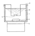
図1は本実施例に用いられた単結晶基板食刻装置を示す模式断面図、図2はZnSe単結晶基板を食刻した後の腐食部分を示す顕微鏡写真で同図(a)は400倍、同図(b)は1000倍に拡大したものであって、これらを参照して以下説明する。
【0013】
あらかじめ高圧溶融法によって得られたZnSe単結晶体から(100)面をスライスして5mm角×1mm厚の基板を切り取り、該基板の表面を研磨した後、鏡面エッチング処理を施したものを供試基板とした。
【0014】
図1に示す単結晶基板食刻装置の反応槽1に入れられた常温(約20℃)の1容積%臭素メタノール溶液6に上記ZnSe基板5が浸漬するようにテフロン製バスケット2に入れて反応槽中にセットした。
【0015】
反応槽底部にはあらかじめ攪拌子3が設けられてあり、反応槽下部にあるマグネチックスターラー4で撹拌子3を250rpm の速度で120秒回転させ、食刻処理を行った。
【0016】
上記食刻処理を施したZnSe基板を反応槽より取り出し、メタノール中で超音波洗浄し乾燥した後、ノマルスキー微分干渉顕微鏡で腐食部分(転位部分)を観察した。
【0017】
観察したZnSe基板上の転位部分を図2(a)の400倍、同図(b)の1000倍の写真として示したが、これらから単位面積当りの転位密度を容易に計測することができた。
【0018】
なお、ZnSe以外のII-VI 族化合物半導体単結晶についても食刻処理を試みたが、ZnSeの場合とほぼ同様の結果が得られた。
【0019】
【発明の効果】
以上説明したように、従来II-VI 族化合物半導体単結晶の(100)面における転位密度を直接計測する手段がなかったが、本発明の方法によれば、簡易な装置を用いて(100)面に食刻処理を施すことにより明確鮮明になった転位を計測できるので、短時間で(100)面の転位密度が測定され、II-VI 族半導体のエピタキシャル成長基板としての適否が容易に判断できるようになった。
【図面の簡単な説明】
【図1】実施例に用いられた単結晶基板食刻装置を示す模式断面図である。
【図2】ZnSe単結晶基板を食刻した後の腐食部分を示す顕微鏡写真で(a)は400倍、(b)は1000倍の拡大写真である。
【符号の説明】
1 反応槽
2 バスケット
3 攪拌子
4 マグネチックスターラー
5 ZnSe基板
6 臭素メタノール溶液
Claims (2)
- ZnSe単結晶体の(100)面をスライスして得た基板に、表面研磨および鏡面エッチング処理を施した後、臭素メタノール溶液に浸漬することによって食刻せしめ、得られた食刻像から該(100)面上の転位を計測することを特徴とするZnSe単結晶体の転位密度測定方法。
- 前記臭素メタノール溶液が0 . 1〜1容積%の臭素メタノール溶液である、請求項1記載のZnSe単結晶体の転位密度測定方法。
Priority Applications (1)
| Application Number | Priority Date | Filing Date | Title |
|---|---|---|---|
| JP14392395A JP3661801B2 (ja) | 1995-05-18 | 1995-05-18 | Ii−vi 族化合物半導体単結晶体の転位密度測定方法 |
Applications Claiming Priority (1)
| Application Number | Priority Date | Filing Date | Title |
|---|---|---|---|
| JP14392395A JP3661801B2 (ja) | 1995-05-18 | 1995-05-18 | Ii−vi 族化合物半導体単結晶体の転位密度測定方法 |
Publications (2)
| Publication Number | Publication Date |
|---|---|
| JPH08316586A JPH08316586A (ja) | 1996-11-29 |
| JP3661801B2 true JP3661801B2 (ja) | 2005-06-22 |
Family
ID=15350249
Family Applications (1)
| Application Number | Title | Priority Date | Filing Date |
|---|---|---|---|
| JP14392395A Expired - Fee Related JP3661801B2 (ja) | 1995-05-18 | 1995-05-18 | Ii−vi 族化合物半導体単結晶体の転位密度測定方法 |
Country Status (1)
| Country | Link |
|---|---|
| JP (1) | JP3661801B2 (ja) |
Families Citing this family (3)
| Publication number | Priority date | Publication date | Assignee | Title |
|---|---|---|---|---|
| FR2813392B1 (fr) * | 2000-08-28 | 2002-12-06 | Snecma Moteurs | Procede de revelation structurale pour superalliages monocristallins |
| KR20120092673A (ko) * | 2009-11-18 | 2012-08-21 | 쓰리엠 이노베이티브 프로퍼티즈 컴파니 | Ⅱ-ⅵ족 반도체를 위한 신규한 습식 에칭제 및 방법 |
| CN114184613A (zh) * | 2021-12-07 | 2022-03-15 | 江苏天鼎检测科技有限公司 | 一种能够清晰显示出碳化物的方法 |
-
1995
- 1995-05-18 JP JP14392395A patent/JP3661801B2/ja not_active Expired - Fee Related
Also Published As
| Publication number | Publication date |
|---|---|
| JPH08316586A (ja) | 1996-11-29 |
Similar Documents
| Publication | Publication Date | Title |
|---|---|---|
| JP3491402B2 (ja) | 単結晶製造方法及びその単結晶製造装置 | |
| EP2733239B1 (en) | Sic single crystal and manufacturing process therefor | |
| JPH05262599A (ja) | SiC単結晶およびその成長方法 | |
| CA2519885A1 (en) | Indium phosphide substrate, indium phosphide single crystal and process for producing them | |
| US11319646B2 (en) | Gallium arsenide single crystal substrate | |
| US12247318B2 (en) | Method for producing SiC single crystal and method for suppressing dislocations in SiC single crystal | |
| WO2023209867A1 (ja) | Iii-v族化合物半導体単結晶基板およびその製造方法 | |
| JP3491429B2 (ja) | 炭化珪素単結晶の製造方法 | |
| EP1420440B1 (en) | An epitaxial wafer and a method for producing it | |
| JP3661801B2 (ja) | Ii−vi 族化合物半導体単結晶体の転位密度測定方法 | |
| JPH0797299A (ja) | SiC単結晶の成長方法 | |
| JPH0977595A (ja) | 炭化珪素単結晶の製造方法 | |
| US20060260536A1 (en) | Vessel for growing a compound semiconductor single crystal, compound semiconductor single crystal, and process for fabricating the same | |
| JP4184622B2 (ja) | 炭化珪素単結晶インゴットの製造方法 | |
| JP2003068744A (ja) | シリコンウエーハの製造方法及びシリコンウエーハ並びにsoiウエーハ | |
| JP3872838B2 (ja) | 結晶成長方法 | |
| JP4200690B2 (ja) | GaAsウェハの製造方法 | |
| JPH09199559A (ja) | 半導体単結晶膜の結晶欠陥評価方法 | |
| JP3560180B2 (ja) | ZnSeホモエピタキシャル単結晶膜の製造法 | |
| JP2004099390A (ja) | 化合物半導体単結晶の製造方法及び化合物半導体単結晶 | |
| JPH10297997A (ja) | 炭化珪素単結晶の製造方法 | |
| JPH10152393A (ja) | バルク結晶の成長方法及びバルク結晶成長用種結晶 | |
| JP3969319B2 (ja) | 燐化物単結晶ウェーハの評価方法 | |
| JP6989897B2 (ja) | タンタル酸リチウム結晶における転位評価方法 | |
| JP2023145595A (ja) | リン化インジウム基板及び半導体エピタキシャルウエハ |
Legal Events
| Date | Code | Title | Description |
|---|---|---|---|
| A131 | Notification of reasons for refusal |
Free format text: JAPANESE INTERMEDIATE CODE: A131 Effective date: 20040127 |
|
| RD02 | Notification of acceptance of power of attorney |
Free format text: JAPANESE INTERMEDIATE CODE: A7422 Effective date: 20040206 |
|
| RD04 | Notification of resignation of power of attorney |
Free format text: JAPANESE INTERMEDIATE CODE: A7424 Effective date: 20040318 |
|
| A521 | Written amendment |
Free format text: JAPANESE INTERMEDIATE CODE: A523 Effective date: 20040326 |
|
| TRDD | Decision of grant or rejection written | ||
| A01 | Written decision to grant a patent or to grant a registration (utility model) |
Free format text: JAPANESE INTERMEDIATE CODE: A01 Effective date: 20050315 |
|
| A61 | First payment of annual fees (during grant procedure) |
Free format text: JAPANESE INTERMEDIATE CODE: A61 Effective date: 20050316 |
|
| R150 | Certificate of patent or registration of utility model |
Free format text: JAPANESE INTERMEDIATE CODE: R150 |
|
| FPAY | Renewal fee payment (event date is renewal date of database) |
Free format text: PAYMENT UNTIL: 20080401 Year of fee payment: 3 |
|
| S531 | Written request for registration of change of domicile |
Free format text: JAPANESE INTERMEDIATE CODE: R313531 |
|
| S533 | Written request for registration of change of name |
Free format text: JAPANESE INTERMEDIATE CODE: R313533 |
|
| FPAY | Renewal fee payment (event date is renewal date of database) |
Free format text: PAYMENT UNTIL: 20080401 Year of fee payment: 3 |
|
| R350 | Written notification of registration of transfer |
Free format text: JAPANESE INTERMEDIATE CODE: R350 |
|
| FPAY | Renewal fee payment (event date is renewal date of database) |
Free format text: PAYMENT UNTIL: 20090401 Year of fee payment: 4 |
|
| FPAY | Renewal fee payment (event date is renewal date of database) |
Free format text: PAYMENT UNTIL: 20090401 Year of fee payment: 4 |
|
| FPAY | Renewal fee payment (event date is renewal date of database) |
Free format text: PAYMENT UNTIL: 20100401 Year of fee payment: 5 |
|
| FPAY | Renewal fee payment (event date is renewal date of database) |
Free format text: PAYMENT UNTIL: 20110401 Year of fee payment: 6 |
|
| LAPS | Cancellation because of no payment of annual fees |