JP3673435B2 - Package for storing semiconductor elements - Google Patents
Package for storing semiconductor elements Download PDFInfo
- Publication number
- JP3673435B2 JP3673435B2 JP27689099A JP27689099A JP3673435B2 JP 3673435 B2 JP3673435 B2 JP 3673435B2 JP 27689099 A JP27689099 A JP 27689099A JP 27689099 A JP27689099 A JP 27689099A JP 3673435 B2 JP3673435 B2 JP 3673435B2
- Authority
- JP
- Japan
- Prior art keywords
- signal
- notch
- signal lead
- terminal
- substrate
- Prior art date
- Legal status (The legal status is an assumption and is not a legal conclusion. Google has not performed a legal analysis and makes no representation as to the accuracy of the status listed.)
- Expired - Fee Related
Links
Images

Landscapes
- Lead Frames For Integrated Circuits (AREA)
Description
【0001】
【発明の属する技術分野】
本発明は、IC,LSI等の半導体素子を収納するための半導体素子収納用パッケージに関する。
【0002】
【従来の技術】
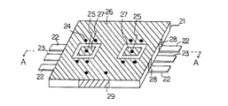
従来の半導体素子収納用パッケージ(以下、半導体パッケージという)を図5および図6に示す。これらの図において、21はアルミナセラミックス等の誘電体材料から成り、半導体パッケージの本体を成す誘電体基板、22は、誘電体基板21の半導体素子の載置面(上面)と反対側の面(下面)に接合され、スルーホール24を通して接地用メタライズ層26に接続された接地用端子、23は、誘電体基板21の下面に接合され、スルーホール25を通して信号用メタライズ層27に接続された信号用リード端子、24は接地用のスルーホール、25は信号用のスルーホールである。
【0003】
また、26は、誘電体基板21の半導体素子の載置面に被着形成された接地用メタライズ層、27は、半導体素子の入出力用の電極と結線されるボンディングワイヤ等の信号線接続用の信号用メタライズ層、28は、誘電体基板21の側端面に被着形成され、接地用端子22に接続された接地用側面メタライズ層、29は、誘電体基板21の他の側端面に被着形成されて電磁シールド用として機能する接地用側面メタライズ層である。
【0004】
そして、IC,LSI等の半導体素子は、誘電体基板21の上面中央部の接地用メタライズ層26上に載置固定され、その入出力用の電極は、フリップチップ接続構造,ボンディングワイヤ等の信号線により信号用メタライズ層27と接続される。なお、半導体素子が載置された誘電体基板21上面の周縁部に、蓋体の周縁部を接合して封止する場合もあるがその蓋体については図示していない。
【0005】
また、他の従来例として、RF(Radio Frequency :高周波)信号入出力端子に対応する部分が誘電体で形成された基板と、基板上にマイクロ波集積回路を囲むように設けられ、少なくともRF信号入出力端子に対応する部分が誘電体で形成される蓋体が被せられた壁体とを備えて成るマイクロ波パッケージにおいて、RF信号入出力端子に壁体の誘電体に対してギャップを設けることにより、RF信号入出力端子のストリップ線路間の結合容量によりRF信号の伝搬をさせて、抵抗の増大を防止し伝搬損が低減するものが提案されている(従来例1:特開平5−3401号公報)。
【0006】
【発明が解決しようとする課題】
しかしながら、図5,図6に示した従来例においては、誘電体基板21に接地用のスルーホール24を形成した構成となっているため、高周波信号用の半導体パッケージでは、スルーホール24とスルーホール25との間に誘電体が存在しており、そのため電磁シールド性が劣化し、高周波信号の誘電体による挿入損失(インサーションロス:insertion loss)が発生していた。
【0007】
また、外部の高周波信号等の電磁波に対する電磁シールドとして、誘電体基板21の側端面に接地用側面メタライズ層29を形成することで、電磁シールド性を強化することは可能だが、この接地用側面メタライズ層29は誘電体基板21の側端面に部分的にしか形成できなかった。それは、このような誘電体基板21は大きな母基板から多数個取りして製造することが多く、その場合キャスタレーション部にのみメタライズ層の被着が可能なためである。さらに、個々の誘電体基板21を母基板から分割した後に、誘電体基板21の側端面にメタライズ層用の金属ペーストを印刷塗布することは作業性が悪く、製造工程において手間が掛かり時間的ロスも大きいため、生産性および歩留りの低下を招いていた。
【0008】
上記従来例1においては、高周波信号がスルーホール間において漏出することにより、アイソレーションおよびインサーションのロスが増大していた。即ち、誘電体端面に高周波信号が漏出し、さらに外部からのノイズが容易に侵入して使用する高周波信号に影響を及ぼして損失を増大させていた。
【0009】
従って、本発明は上記事情に鑑みて完成されたものであり、その目的は、信号用のスルーホールと接地用のスルーホール間に存在する誘電体による電磁シールド性の劣化を抑制して高周波信号の挿入損失を小さくし、高周波信号の伝搬速度を向上させるとともに、製造時の作業性を向上させて生産性及び製造歩留りを良好なものとすることにある。
【0010】
【課題を解決するための手段】
本発明の半導体素子収納用パッケージは、上面の中央部に半導体素子の搭載部を、上面の周縁部にその上下を貫通する端子部材嵌着用の切欠部を有する金属基板と、該金属基板の前記切欠部と略同じ大きさの誘電体基板に、上下面を貫通する貫通導体が形成されるとともに、上下面にそれぞれ前記貫通導体に接続された信号用メタライズ層が形成され、かつ下面側の前記信号用メタライズ層に前記誘電体基板の外側に延びる信号用リード端子が接合されるとともに、下面側の前記信号用メタライズ層および前記信号用リード端子の周囲から周縁部にかけてメタライズ層が被着され、さらに前記信号用リード端子が外側に延びる側の側面に隣接する両側面にメタライズ層が被着されて成り、前記信号用リード端子が前記切欠部から前記金属基板の外側へ延びるように前記切欠部に嵌着された端子部材と、前記金属基板の下面に前記端子部材の前記信号用リード端子をそれぞれ切欠部側で取り囲むように接合されるとともに、該信号用リード端子に隣接して略平行に配設される接地用リード端子を有する接地金属板とを具備することを特徴とする。
【0011】
本発明は、上記構成により、信号経路と接地電位部との間に存在する誘電体が少なくなるように構成することで、信号経路部と接地電位部とが誘電体を介して電磁結合,容量結合し電磁シールド性が劣化するのを抑制して、高周波信号の損失を小さくするとともに高周波信号の伝搬速度を向上させることができる。また、製造時の作業性を向上させて生産性及び製造歩留りを良好なものとするという作用効果も有する。
【0012】
また本発明の半導体素子収納用パッケージは、内側に半導体素子を収容するとともに、側部の下面にその側部を貫通する切欠部を有する金属枠体と、該金属枠体の前記切欠部と同じ断面積を有する誘電体基板に、上下面を貫通する貫通導体が形成されるとともに、上下面にそれぞれ前記貫通導体に接続された信号用メタライズ層が形成され、かつ下面側の前記信号用メタライズ層に前記誘電体基板の外側に延びる信号用リード端子が接合されるとともに、下面側の前記信号用メタライズ層および前記信号用リード端子の周囲から周縁部にかけてメタライズ層が被着され、さらに前記信号用リード端子が外側に延びる側の側面に隣接する両側面にメタライズ層が被着されて成り、前記信号用リード端子が前記切欠部から前記金属枠体の外側へ延びるように前記切欠部に嵌着された端子部材と、前記金属枠体の下面に前記端子部材の前記信号用リード端子をそれぞれ切欠部側で取り囲むように接合されるとともに、該信号用リード端子に隣接して略平行に配設される接地用リード端子を有し、かつその上面の中央部に前記半導体素子の搭載部を設けた金属基板とを具備することを特徴とする。
【0013】
このような構成により、上記電磁シールド性の向上効果に加え、端子部材を設置するための金属板が一枚で済み、さらに簡易で低コスト化された構成となり、また半導体素子を金属枠体で囲まれた空間内に収納することができるため全体が低背化される。
【0014】
【発明の実施の形態】
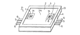
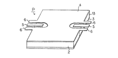
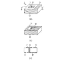
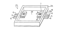
本発明の半導体パッケージPを図1〜図4に示す。図1は半導体パッケージPの上面側の斜視図、図2は半導体パッケージPの下面側の斜視図、図3(a)は半導体パッケージP用の端子部材の上面側の斜視図、図3(b)は前記端子部材の下面側の斜視図、図3(c)は(a)のB−B線における断面図、図4は本発明の他の実施形態による半導体パッケージP1の上面側の斜視図である。
【0015】
図1〜図3において、1は上下面を貫通するスルーホール,ビアホール等の貫通導体8が形成され、かつ該貫通導体8に接続して上下面にそれぞれ形成された信号用メタライズ層7,12を有する信号入力用の端子部材と信号出力用の端子部材であり、2は、上面の中央部に半導体素子の搭載部2aを、上面の周縁部に上下を貫通する端子部材1,1嵌着用の2つの切欠部1a,1aを有する金属基板である。また、3は、金属基板2の上面周辺部にロウ材等により接合される蓋体封止用のシールリングとしての金属枠体、4は、金属基板2の下面に端子部材1,1の信号用リード端子5,5を切欠部1a,1a側で取り囲むように接合されるとともに、信号用リード端子5,5に隣接して略平行に配設される接地用リード端子6を有する接地金属板である。
【0016】
また、5は、端子部材1,1の各々の下面側の信号用メタライズ層12に接合され、切欠部1a,1aと略同じ大きさの端子部材1,1用の誘電体基板の外側に延びる信号用リード端子、6は、各信号用リード端子5,5の両側に隣接して略平行に形成された接地用リード端子、7は、貫通導体8に接続して端子部材1上面に形成された信号用メタライズ層、8は、スルーホール,ビアホール等の貫通導体、13は、金属基板2の側面全体に被着され金属枠体3を金属基板2に接合させるためのメタライズ層である。なお、金属基板2の上面の中央部に半導体素子を載置させた後、金属枠体3上面に蓋体の周縁部を接合して封止するが、その蓋体については図示していない。
【0017】
本発明において、端子部材1,1はアルミナ(Al2 O3 )セラミックス,窒化アルミニウム(AlN)セラミックス,ムライト(3Al2 O3 ・2SiO2 )セラミックス,炭化珪素(SiC)セラミックス,フォルステライト(2MgO・SiO2 )セラミックス,ジルコニア(ZrO2 )セラミックス,ステアタイト(3MgO・4SiO2 ・H2 O)セラミックス,コーディエライト(2MgO・2Al2 O3 ・5SiO2 )セラミックス,ベリリア(BeO)セラミックス,石英,ガラス,ガラスセラミックス等の誘電体基板から成るのが良く、これらは高周波信号の誘電体損失(tanδ)が小さい。端子部材1,1は、金属基板2にそれらの相補形状に形成された切欠部1aに嵌合され、金属ロウ材等により接合される。
【0018】
また、図3(a)に示すように、端子部材1は、その上面の信号用リード端子5側の辺縁部に金属枠体3と接合させるためのメタライズ層9が被着され、その上面中央部には、上下面を貫通する貫通導体8と貫通導体8に接続して形成された信号用メタライズ層7を有する。端子部材1の信号用リード端子5側の側面に隣接する両側面には、金属基板2と接合させるためのメタライズ層10が被着される。また、同図(b),(c)に示すように、端子部材1の下面には、中心部より信号用リード端子5側の端部へ延びるように形成され信号用リード端子5に接続される信号用メタライズ層12と、信号用メタライズ層12の周囲から周縁部にかけて形成されるメタライズ層11とが被着されており、端子部材1の下面の中央部において信号用メタライズ層12が貫通導体8に接続される。
【0019】
この端子部材1は、図3の如く直方体状とされているが、直方体状に限らず円柱状,三角柱状等の多角柱状,錐状台形状等種々の形状とし得る。即ち、金属基板2の上下面で露出する面を有する形状であれば良い。
【0020】
金属基板2,接地金属板4および金属枠体3の材料は、銅(Cu)−タングステン(W)合金,SUS(ステンレス),鉄(Fe)−ニッケル(Ni)−コバルト(Co)合金(コバール),鉄(Fe)−ニッケル(Ni)合金,その他Cu−Mo,Cu,Ni,Mo,Fe,またはCuを主成分とするCu系合金等が好ましく、これらは電磁遮蔽(電磁シールド)性に優れる。
【0021】
本実施形態では、信号用リード端子5は、接地金属板4の主面方向に沿って半導体パッケージから外側に延びるように設けられているが、接地金属板4の主面に垂直な方向に沿って外側、例えば下側に延びるように設けても良い。その場合、接地用リード端子6も、接地金属板4の主面に垂直な方向に沿って信号用リード端子5に略平行に設けることができる。また、接地用リード端子6は信号用リード端子5の両側に隣接して略平行に設けられているが、信号用リード端子5の片側にのみ接地用リード端子6を設けることもできる。但し、信号用リード端子5の両側に接地用リード端子6を設けた方が好ましく、信号の損失が小さく伝送特性が良好となる。
【0022】
本発明の信号用メタライズ層7,12、およびメタライズ層9,10,11,13は、公知のW,Mo−Mn,Pd,Pt,Ti,Au等の金属または合金の粒子を含有する金属ペーストを塗布し焼成する、またはスパッタリング法によって被着形成される。Mo−Mnペーストを塗布焼成したものの場合、Niメッキを施し、Ag−Cu共晶合金ロウ材により他の部材と接合するか、またはNiメッキ,Auメッキを施し、Au−Sn合金ロウ材により他の部材と接合する。また、Ti層,Pt層,Au層の3層をスパッタリング法により成膜したものの場合、Au−Sn合金ロウ材により他の部材と接合する。
【0023】
貫通導体8はスルーホール,ビアホール等であり、端子部材1の所定の箇所に貫通孔を形成し、その貫通孔の内面に上記メタライズ層と同様に金属ペーストを塗布し焼成するか、または金属メッキ層を形成することによって、スルーホールが作製される。また、ビアホールとする場合、前記貫通孔の内部に金属ペーストを充填して焼成する、または貫通孔の内部に金属ペーストを充填焼成後さらに溶融金属を充填させるといった方法により形成し得る。
【0024】
本発明の第二の実施形態として、図4に示すような構成とし得る。この第二の実施形態では、図1の金属基板2がない代わりに、内側に半導体素子を収容するとともに側部を貫通する2つの切欠部14,14を有する金属枠体3aを設けたものである。また、金属枠体3aの切欠部14と同じ断面積を有する端子部材1が、切欠部14,14に嵌着されており、さらに金属枠体3aの下面に端子部材1,1の信号用リード端子5をそれぞれ切欠部14側で取り囲むように接合されるとともに、信号用リード端子5に隣接して略平行に配設される接地用リード端子6を有し、かつその上面の中央部に半導体素子の搭載部4bを設けた金属基板4aを具備する構成であり、他の構成は図1のものと同様である。この第二の実施形態によると、図1の金属基板2が不要となり、構成が簡易化されて低コストに製造可能となり、また金属枠体3aで囲まれた空間内に半導体素子を収納することができるので、全体が低背化されるものである。
【0025】
この第二の実施形態において、端子部材1の切欠部14に嵌着される部分は、切欠部14と同じ断面積を有しているが、それ以外の部分は切欠部14と全く同じ形状、大きさをしている必要はなく、例えば金属枠体3aから外側に端子部材1の一部が突出していても構わない。
【0026】
また、図1,図4の実施形態において、切欠部1a,切欠部14はそれぞれ2つあるが、2つに限らず、1つまたは2つ以上設けることができる。
【0027】
本発明において、信号用リード端子5と接地用リード端子6との間隔を、使用する高周波信号の波長の32分の1以上とすることが好ましく、波長の32分の1未満の場合、信号用リード端子5と接地用リード端子6とが容量結合,電磁結合し易くなり、高周波信号の損失が増大する。また、本発明の半導体パッケージは、10GHz以上の高周波帯域で使用するものに適している。
【0028】
かくして、本発明は、信号経路と接地電位部との間に存在する誘電体が少なくなるように構成することで、信号経路部と接地電位部とが誘電体を介して電磁結合,容量結合し電磁シールド性が劣化するのを抑制して、高周波信号の挿入損失を小さくするとともに高周波信号の伝搬速度を向上させ得る。また、製造時の作業性を向上させて生産性及び製造歩留りが高まるという作用効果も有する。
【0029】
尚、本発明は上記の実施形態に限定されるものではなく、本発明の要旨を逸脱しない範囲内で種々の変更は何等差し支えない。
【0030】
【発明の効果】
本発明は、上面の中央部に半導体素子の搭載部を、上面の周縁部にその上下を貫通する端子部材嵌着用の切欠部を有する金属基板と、前記切欠部と略同じ大きさの誘電体基板に、上下面を貫通する貫通導体が形成され、上下面にそれぞれ貫通導体に接続された信号用メタライズ層が形成され、かつ下面側の信号用メタライズ層に誘電体基板の外側に延びる信号用リード端子が接合されるとともに、下面側の信号用メタライズ層および信号用リード端子の周囲から周縁部にかけてメタライズ層が被着され、さらに信号用リード端子が外側に延びる側の側面に隣接する両側面にメタライズ層が被着されて成り、信号用リード端子が切欠部から金属基板の外側へ延びるように切欠部に嵌着された端子部材と、金属基板の下面に信号用リード端子をそれぞれ切欠部側で取り囲むように接合されるとともに、信号用リード端子に隣接して略平行に配設される接地用リード端子を有する接地金属板と、を具備することにより、信号経路部と接地電位部とが誘電体を介して電磁結合、容量結合し電磁シールド性が劣化するのを抑制し、高周波信号の挿入損失を小さくするとともに高周波信号の伝搬速度を向上させ、また製造時の作業性を向上させて生産性及び製造歩留りが高いものとなる。
【0031】
また本発明は、内側に半導体素子を収容するとともに、側部の下面にその側部を貫通する切欠部を有する金属枠体と、前記切欠部と同じ断面積を有する誘電体基板に、上下面を貫通する貫通導体が形成され、上下面にそれぞれ貫通導体に接続された信号用メタライズ層が形成され、かつ下面側の信号用メタライズ層に誘電体基板の外側に延びる信号用リード端子が接合されるとともに、下面側の信号用メタライズ層および信号用リード端子の周囲から周縁部にかけてメタライズ層が被着され、さらに信号用リード端子が外側に延びる側の側面に隣接する両側面にメタライズ層が被着されて成り、信号用リード端子が切欠部から金属枠体の外側へ延びるように切欠部に嵌着された端子部材と、金属枠体の下面に信号用リード端子をそれぞれ切欠部側で取り囲むように接合されるとともに、信号用リード端子に隣接して略平行に配設される接地用リード端子を有し、かつその上面の中央部に半導体素子の搭載部を設けた金属基板と、を具備することにより、上記の電磁シールド性の向上効果に加え、端子部材を設置するための金属板が一枚で済み、さらに簡易で低コスト化された構成となり、また半導体素子を金属枠体で囲まれた空間内に収納することができるため全体が低背化されるという作用効果を有する。
【図面の簡単な説明】
【図1】本発明の半導体パッケージの上面側の斜視図である。
【図2】本発明の半導体パッケージの下面側の図である。
【図3】本発明の半導体パッケージ用の端子部材を示し、(a)は端子部材の上面側の斜視図、(b)は端子部材の下面側の斜視図、(c)は(a)のB−B線における断面図である。
【図4】本発明の第二の実施形態による半導体パッケージの上面側の斜視図である。
【図5】従来の半導体パッケージの上面側の斜視図である。
【図6】図5のA−A線における断面図である。
【符号の説明】
1:端子部材
2:金属基板
3:金属枠体
3a:金属枠体
4:接地金属板
5:信号用リード端子
6:接地用リード端子
7:信号用メタライズ層
8:貫通導体
12:信号用メタライズ層[0001]
BACKGROUND OF THE INVENTION
The present invention relates to a semiconductor element housing package for housing semiconductor elements such as ICs and LSIs.
[0002]
[Prior art]
A conventional semiconductor element storage package (hereinafter referred to as a semiconductor package) is shown in FIGS. In these drawings,
[0003]
[0004]
A semiconductor element such as an IC or LSI is mounted and fixed on the
[0005]
As another conventional example, a portion corresponding to an RF (Radio Frequency) signal input / output terminal is provided with a substrate formed of a dielectric, and a microwave integrated circuit is provided on the substrate so as to surround at least an RF signal. In a microwave package comprising a wall body covered with a lid whose portion corresponding to an input / output terminal is formed of a dielectric, a gap is provided to the RF signal input / output terminal with respect to the dielectric of the wall body Therefore, an RF signal is propagated by a coupling capacitance between strip lines of an RF signal input / output terminal to prevent an increase in resistance and reduce propagation loss (conventional example 1: Japanese Patent Laid-Open No. 5-3401). Issue gazette).
[0006]
[Problems to be solved by the invention]
However, since the conventional example shown in FIGS. 5 and 6 has a structure in which the grounding through hole 24 is formed in the
[0007]
In addition, although the grounding
[0008]
In Conventional Example 1, the loss of isolation and insertion has increased due to leakage of high-frequency signals between through holes. That is, a high-frequency signal leaks to the dielectric end face, and noise from the outside easily penetrates and affects the high-frequency signal to be used, thereby increasing the loss.
[0009]
Therefore, the present invention has been completed in view of the above circumstances, and an object of the present invention is to suppress the deterioration of the electromagnetic shielding property due to the dielectric existing between the signal through hole and the ground through hole. The insertion loss is reduced, the propagation speed of the high-frequency signal is improved, and the workability at the time of manufacturing is improved to improve the productivity and the manufacturing yield.
[0010]
[Means for Solving the Problems]
The package for housing a semiconductor element of the present invention includes a metal substrate having a semiconductor element mounting portion at the center of the upper surface and a notch for fitting a terminal member passing through the upper and lower peripheral portions of the upper surface. A dielectric substrate having substantially the same size as the notch is formed with a through conductor penetrating the upper and lower surfaces, a signal metallization layer connected to the through conductor is formed on the upper and lower surfaces, respectively, and wherein the signal supplying metallized layer dielectric substrate signal lead terminals extending outwardly are joined in Rutotomoni, metallized layer from the periphery of the signal metallization layer and the signal lead terminals on the lower surface side to the peripheral portion is deposited, become more metallized layers on both side faces the signal lead terminal is adjacent to the side of the side extending outwardly is deposited, the metal substrate wherein the signal lead terminals from said notch A terminal member fitted into the notch so as to extend outward, and a signal lead connected to the lower surface of the metal substrate so as to surround the signal lead terminal of the terminal member on the notch side. And a ground metal plate having a ground lead terminal disposed substantially parallel to the terminal.
[0011]
The present invention is configured so that the dielectric existing between the signal path and the ground potential part is reduced by the above configuration, so that the signal path part and the ground potential part are electromagnetically coupled and capacitance via the dielectric. It is possible to suppress the deterioration of the electromagnetic shielding properties by coupling, thereby reducing the loss of the high frequency signal and improving the propagation speed of the high frequency signal. In addition, there is an effect that the workability at the time of manufacturing is improved to improve the productivity and the manufacturing yield.
[0012]
The package for housing a semiconductor element of the present invention houses a semiconductor element inside, and has a metal frame having a notch passing through the side on the lower surface of the side, and the same as the notch of the metal frame A dielectric substrate having a cross-sectional area is formed with through conductors penetrating the upper and lower surfaces, signal metallization layers connected to the through conductors are respectively formed on the upper and lower surfaces, and the signal metallization layer on the lower surface side said dielectric signal lead terminals extending outwardly of the substrate is bonded Rutotomoni, metallized layer is deposited from a periphery of the signal metallization layer and the signal lead terminals on the lower surface side to the peripheral portion, for further the signal become metallized layer on both side surfaces lead terminal adjacent to the side of the side extending outwardly is deposited, extending the signal lead terminals to the outside of the metal frame from the notch A terminal member fitted in the cutout portion, and the signal lead terminal of the terminal member so as to surround each of the signal lead terminals of the terminal member on the lower surface of the metal frame body on the cutout portion side. And a metal substrate provided with a mounting portion for mounting the semiconductor element at the center of the upper surface thereof.
[0013]
With such a configuration, in addition to the above-described effect of improving the electromagnetic shielding properties, only one metal plate is required for installing the terminal member, and the configuration is further simplified and reduced in cost, and the semiconductor element is made of a metal frame. Since it can be stored in the enclosed space, the overall height is reduced.
[0014]
DETAILED DESCRIPTION OF THE INVENTION
A semiconductor package P of the present invention is shown in FIGS. 1 is a perspective view of the upper surface side of the semiconductor package P, FIG. 2 is a perspective view of the lower surface side of the semiconductor package P, FIG. 3A is a perspective view of the upper surface side of the terminal member for the semiconductor package P, and FIG. ) Is a perspective view of the lower surface side of the terminal member, FIG. 3C is a sectional view taken along line BB of FIG. 4A, and FIG. 4 is a perspective view of the upper surface side of the semiconductor package P1 according to another embodiment of the present invention. It is.
[0015]
In FIG. 1 to FIG. 3, reference numeral 1 denotes a
[0016]
Further, 5 is joined to the
[0017]
In the present invention, the terminal members 1 and 1 are made of alumina (Al 2 O 3 ) ceramics, aluminum nitride (AlN) ceramics, mullite (3Al 2 O 3 .2SiO 2 ) ceramics, silicon carbide (SiC) ceramics, forsterite (2MgO.multidot. SiO 2) ceramics, zirconia (ZrO 2) ceramics, steatite (3MgO · 4SiO 2 · H 2 O) ceramics, cordierite (2MgO · 2Al 2 O 3 · 5SiO 2) ceramics, beryllia (BeO) ceramic, quartz, It is preferable to be made of a dielectric substrate such as glass or glass ceramic, which has a low dielectric loss (tan δ) of a high-frequency signal. The terminal members 1 and 1 are fitted into a notch 1a formed in a complementary shape on the metal substrate 2 and joined by a metal brazing material or the like.
[0018]
Further, as shown in FIG. 3A, the terminal member 1 has a metallized layer 9 attached to the edge of the upper surface of the terminal member 1 on the signal lead terminal 5 side to be bonded to the
[0019]
Although this terminal member 1 is formed in a rectangular parallelepiped shape as shown in FIG. 3, it is not limited to a rectangular parallelepiped shape, but may have various shapes such as a columnar shape, a polygonal columnar shape such as a triangular prism shape, and a truncated cone shape. That is, any shape having a surface exposed on the upper and lower surfaces of the metal substrate 2 may be used.
[0020]
The materials of the metal substrate 2, the ground metal plate 4 and the
[0021]
In the present embodiment, the signal lead terminal 5 is provided so as to extend outward from the semiconductor package along the main surface direction of the ground metal plate 4, but along the direction perpendicular to the main surface of the ground metal plate 4. It may be provided so as to extend outward, for example, downward. In this case, the
[0022]
The
[0023]
The through
[0024]
As a second embodiment of the present invention, a configuration as shown in FIG. 4 may be adopted. In the second embodiment, instead of the metal substrate 2 of FIG. 1, a metal frame 3 a having two
[0025]
In this second embodiment, the portion fitted into the
[0026]
In the embodiment of FIGS. 1 and 4, there are two
[0027]
In the present invention, the distance between the signal lead terminal 5 and the
[0028]
Thus, the present invention is configured such that the dielectric existing between the signal path and the ground potential part is reduced, so that the signal path part and the ground potential part are electromagnetically coupled and capacitively coupled via the dielectric. It is possible to suppress the deterioration of the electromagnetic shielding property, reduce the insertion loss of the high frequency signal, and improve the propagation speed of the high frequency signal. In addition, there is an effect that the workability at the time of manufacturing is improved and the productivity and the manufacturing yield are increased.
[0029]
In addition, this invention is not limited to said embodiment, A various change does not interfere in the range which does not deviate from the summary of this invention.
[0030]
【The invention's effect】
The present invention relates to a metal substrate having a semiconductor element mounting portion at the center of the upper surface, a notch portion for fitting a terminal member passing through the upper and lower edges of the upper surface, and a dielectric having approximately the same size as the notch portion. The substrate is formed with through conductors that penetrate the upper and lower surfaces, signal metallization layers connected to the through conductors are formed on the upper and lower surfaces, respectively, and the signal metallization layer on the lower surface side extends outside the dielectric substrate. lead terminals are joined Rutotomoni, metallized layer is deposited from the surrounding lower surface side signal metallization layer and the signal lead terminal toward the peripheral portion, both side surfaces further signal lead terminal is adjacent to the side of the side extending outwardly metallization layer is deposited on become, its a terminal member which is fitted in the notch so that the signal lead terminal extending from the notch to the outside of the metal substrate, a signal lead terminal for the lower surface of the metal substrate A grounding metal plate having a ground lead terminal disposed adjacent to and parallel to the signal lead terminal and being joined so as to surround each of the notch portions. Suppresses electromagnetic shielding and capacitive coupling with the ground potential part via a dielectric, thereby reducing electromagnetic shielding, reducing high-frequency signal insertion loss, improving high-frequency signal propagation speed, and manufacturing operations This improves the productivity and increases the production yield.
[0031]
The present invention also includes a metal frame having a cutout portion penetrating the side portion on the lower surface of the side portion and a dielectric substrate having the same cross-sectional area as the cutout portion. A signal metallization layer connected to the through-conductors is formed on the upper and lower surfaces, and a signal lead terminal extending outside the dielectric substrate is joined to the signal metallization layer on the lower surface side. In addition, the metallization layer is applied from the periphery of the signal metallization layer and the signal lead terminal on the lower surface side to the periphery, and the metallization layer is applied to both side surfaces adjacent to the side surface on the side where the signal lead terminal extends outward. made is wearing, a terminal member that is fitted to the cutout portion so as to extend to the outside of the metal frame from the signal lead terminal notch, the lead terminal signal to the lower surface of the metal frame, respectively notch A metal substrate having a ground lead terminal disposed so as to be adjacent to and in parallel with the signal lead terminal and having a semiconductor element mounting portion at the center of the upper surface thereof. In addition to the above-described effect of improving the electromagnetic shielding properties, a single metal plate for installing the terminal member is sufficient, and the structure is further simplified and reduced in cost, and the semiconductor element is made of metal. Since it can be accommodated in the space surrounded by the frame, it has the effect of reducing the overall height.
[Brief description of the drawings]
FIG. 1 is a perspective view of an upper surface side of a semiconductor package of the present invention.
FIG. 2 is a view of the lower surface side of the semiconductor package of the present invention.
3A and 3B show a terminal member for a semiconductor package according to the present invention, in which FIG. 3A is a perspective view of the upper surface side of the terminal member, FIG. 3B is a perspective view of the lower surface side of the terminal member, and FIG. It is sectional drawing in the BB line.
FIG. 4 is a perspective view of an upper surface side of a semiconductor package according to a second embodiment of the present invention.
FIG. 5 is a top perspective view of a conventional semiconductor package.
6 is a cross-sectional view taken along line AA in FIG.
[Explanation of symbols]
1: Terminal member 2: Metal substrate 3: Metal frame 3a: Metal frame 4: Ground metal plate 5: Signal lead terminal 6: Ground lead terminal 7: Signal metallization layer 8: Through conductor 12: Signal metallization layer
Claims (2)
該金属基板の前記切欠部と略同じ大きさの誘電体基板に、上下面を貫通する貫通導体が形成されるとともに、上下面にそれぞれ前記貫通導体に接続された信号用メタライズ層が形成され、かつ下面側の前記信号用メタライズ層に前記誘電体基板の外側に延びる信号用リード端子が接合されるとともに、下面側の前記信号用メタライズ層および前記信号用リード端子の周囲から周縁部にかけてメタライズ層が被着され、さらに前記信号用リード端子が外側に延びる側の側面に隣接する両側面にメタライズ層が被着されて成り、前記信号用リード端子が前記切欠部から前記金属基板の外側へ延びるように前記切欠部に嵌着された端子部材と、
前記金属基板の下面に前記端子部材の前記信号用リード端子をそれぞれ切欠部側で取り囲むように接合されるとともに、該信号用リード端子に隣接して略平行に配設される接地用リード端子を有する接地金属板とを具備することを特徴とする半導体素子収納用パッケージ。A metal substrate having a semiconductor element mounting portion at the center of the upper surface, and a peripheral portion of the upper surface having a notch for fitting a terminal member that penetrates the upper and lower sides thereof;
A dielectric substrate having substantially the same size as the notch of the metal substrate is formed with through conductors penetrating the upper and lower surfaces, and a signal metallization layer connected to the through conductors is formed on the upper and lower surfaces, respectively. metallized layer toward the peripheral portion and the lower surface of said the signal metallization layer dielectric signal lead terminals extending outwardly of the substrate is bonded Rutotomoni, from the periphery of the signal metallization layer and the signal lead terminals on the lower surface side There is deposited, become more metallized layers on both side faces the signal lead terminal is adjacent to the side of the side extending outwardly is adhered, the signal lead terminals extending outwardly of the metallic substrate from the notch A terminal member fitted in the notch,
The signal lead terminals of the terminal member are joined to the lower surface of the metal substrate so as to surround each of the notch portions, and ground lead terminals disposed substantially parallel to the signal lead terminals are provided. A package for housing a semiconductor element, comprising: a ground metal plate.
該金属枠体の前記切欠部と同じ断面積を有する誘電体基板に、上下面を貫通する貫通導体が形成されるとともに、上下面にそれぞれ前記貫通導体に接続された信号用メタライズ層が形成され、かつ下面側の前記信号用メタライズ層に前記誘電体基板の外側に延びる信号用リード端子が接合されるとともに、下面側の前記信号用メタライズ層および前記信号用リード端子の周囲から周縁部にかけてメタライズ層が被着され、さらに前記信号用リード端子が外側に延びる側の側面に隣接する両側面にメタライズ層が被着されて成り、前記信号用リード端子が前記切欠部から前記金属枠体の外側へ延びるように前記切欠部に嵌着された端子部材と、
前記金属枠体の下面に前記端子部材の前記信号用リード端子をそれぞれ切欠部側で取り囲むように接合されるとともに、該信号用リード端子に隣接して略平行に配設される接地用リード端子を有し、かつその上面の中央部に前記半導体素子の搭載部を設けた金属基板とを具備することを特徴とする半導体素子収納用パッケージ。A metal frame that houses a semiconductor element on the inside and has a notch penetrating the side on the lower surface of the side,
A dielectric substrate having the same cross-sectional area as the notch of the metal frame is formed with through conductors penetrating the upper and lower surfaces, and signal metallization layers connected to the through conductors are formed on the upper and lower surfaces, respectively. and metallized lower side of said the signal metallization layer dielectric signal lead terminals extending outwardly of the substrate is bonded Rutotomoni, from the periphery of the signal metallization layer and the signal lead terminals on the lower surface side to the peripheral portion layer is deposited, comprises is further deposited metallization layer on both sides by the signal lead terminal is adjacent to the side of the side extending outwardly, outside the metal frame the signal lead terminals from said notch A terminal member fitted into the notch so as to extend to
A ground lead terminal that is joined to the lower surface of the metal frame so as to surround the signal lead terminal of the terminal member on the cutout side, and is disposed substantially parallel to the signal lead terminal. And a metal substrate provided with a mounting portion of the semiconductor element at the center of the upper surface thereof.
Priority Applications (1)
| Application Number | Priority Date | Filing Date | Title |
|---|---|---|---|
| JP27689099A JP3673435B2 (en) | 1999-09-29 | 1999-09-29 | Package for storing semiconductor elements |
Applications Claiming Priority (1)
| Application Number | Priority Date | Filing Date | Title |
|---|---|---|---|
| JP27689099A JP3673435B2 (en) | 1999-09-29 | 1999-09-29 | Package for storing semiconductor elements |
Publications (2)
| Publication Number | Publication Date |
|---|---|
| JP2001102473A JP2001102473A (en) | 2001-04-13 |
| JP3673435B2 true JP3673435B2 (en) | 2005-07-20 |
Family
ID=17575834
Family Applications (1)
| Application Number | Title | Priority Date | Filing Date |
|---|---|---|---|
| JP27689099A Expired - Fee Related JP3673435B2 (en) | 1999-09-29 | 1999-09-29 | Package for storing semiconductor elements |
Country Status (1)
| Country | Link |
|---|---|
| JP (1) | JP3673435B2 (en) |
Families Citing this family (1)
| Publication number | Priority date | Publication date | Assignee | Title |
|---|---|---|---|---|
| JP4761713B2 (en) * | 2004-01-28 | 2011-08-31 | 京セラ株式会社 | Electronic component sealing substrate, multi-component electronic component sealing substrate, and method of manufacturing electronic device |
-
1999
- 1999-09-29 JP JP27689099A patent/JP3673435B2/en not_active Expired - Fee Related
Also Published As
| Publication number | Publication date |
|---|---|
| JP2001102473A (en) | 2001-04-13 |
Similar Documents
| Publication | Publication Date | Title |
|---|---|---|
| US4839717A (en) | Ceramic package for high frequency semiconductor devices | |
| JPH0846073A (en) | Semiconductor device | |
| JPH04336702A (en) | Package | |
| JPH07147352A (en) | Semiconductor integrated circuit device | |
| US5523621A (en) | Semiconductor device having a multilayer ceramic wiring substrate | |
| US10249564B2 (en) | Electronic component mounting substrate, electronic device, and electronic module | |
| JP2001189417A (en) | Semiconductor module package | |
| JP2728322B2 (en) | Semiconductor device | |
| JP3981645B2 (en) | Input/output terminal, semiconductor element storage package, and semiconductor device | |
| JPH11330298A (en) | Package with signal terminal and electronic device using the same | |
| JP2001102473A (en) | Package for storing semiconductor elements | |
| JP4009169B2 (en) | Semiconductor element storage package and semiconductor device | |
| JP2002190540A (en) | Package for storing semiconductor elements | |
| JP4206185B2 (en) | High frequency semiconductor device | |
| JP3398315B2 (en) | Package for storing high-frequency elements | |
| JP6744103B2 (en) | Package for storing semiconductor element and semiconductor device | |
| US7105924B2 (en) | Integrated circuit housing | |
| JP3720726B2 (en) | Semiconductor element storage package and semiconductor device | |
| JP2005285872A (en) | Semiconductor element storage package and semiconductor device | |
| JP2000183488A (en) | Hybrid module | |
| JPH11340370A (en) | High frequency module | |
| JP2004228532A (en) | I / O terminal and semiconductor element storage package and semiconductor device | |
| JP2004349568A (en) | I / O terminal and semiconductor element storage package and semiconductor device | |
| JP4127390B2 (en) | Semiconductor element storage package and semiconductor device | |
| JPH05144953A (en) | Electronic parts storage package |
Legal Events
| Date | Code | Title | Description |
|---|---|---|---|
| A977 | Report on retrieval |
Free format text: JAPANESE INTERMEDIATE CODE: A971007 Effective date: 20041221 |
|
| A131 | Notification of reasons for refusal |
Free format text: JAPANESE INTERMEDIATE CODE: A131 Effective date: 20041228 |
|
| A521 | Request for written amendment filed |
Free format text: JAPANESE INTERMEDIATE CODE: A523 Effective date: 20050228 |
|
| TRDD | Decision of grant or rejection written | ||
| A01 | Written decision to grant a patent or to grant a registration (utility model) |
Free format text: JAPANESE INTERMEDIATE CODE: A01 Effective date: 20050419 |
|
| A61 | First payment of annual fees (during grant procedure) |
Free format text: JAPANESE INTERMEDIATE CODE: A61 Effective date: 20050422 |
|
| R150 | Certificate of patent or registration of utility model |
Free format text: JAPANESE INTERMEDIATE CODE: R150 |
|
| FPAY | Renewal fee payment (event date is renewal date of database) |
Free format text: PAYMENT UNTIL: 20080428 Year of fee payment: 3 |
|
| FPAY | Renewal fee payment (event date is renewal date of database) |
Free format text: PAYMENT UNTIL: 20090428 Year of fee payment: 4 |
|
| FPAY | Renewal fee payment (event date is renewal date of database) |
Free format text: PAYMENT UNTIL: 20090428 Year of fee payment: 4 |
|
| FPAY | Renewal fee payment (event date is renewal date of database) |
Free format text: PAYMENT UNTIL: 20100428 Year of fee payment: 5 |
|
| FPAY | Renewal fee payment (event date is renewal date of database) |
Free format text: PAYMENT UNTIL: 20110428 Year of fee payment: 6 |
|
| FPAY | Renewal fee payment (event date is renewal date of database) |
Free format text: PAYMENT UNTIL: 20110428 Year of fee payment: 6 |
|
| FPAY | Renewal fee payment (event date is renewal date of database) |
Free format text: PAYMENT UNTIL: 20120428 Year of fee payment: 7 |
|
| LAPS | Cancellation because of no payment of annual fees |