JP3732012B2 - DC / DC converter using primary winding of transformer - Google Patents
DC / DC converter using primary winding of transformer Download PDFInfo
- Publication number
- JP3732012B2 JP3732012B2 JP23061298A JP23061298A JP3732012B2 JP 3732012 B2 JP3732012 B2 JP 3732012B2 JP 23061298 A JP23061298 A JP 23061298A JP 23061298 A JP23061298 A JP 23061298A JP 3732012 B2 JP3732012 B2 JP 3732012B2
- Authority
- JP
- Japan
- Prior art keywords
- voltage
- converter
- output
- transistor
- coil
- Prior art date
- Legal status (The legal status is an assumption and is not a legal conclusion. Google has not performed a legal analysis and makes no representation as to the accuracy of the status listed.)
- Expired - Fee Related
Links
Images


Landscapes
- Dc-Dc Converters (AREA)
Description
【0001】
【発明の属する技術分野】
内部にトランスを有するDC/DCコンバータに関するもので、特に、複数の出力を必要とするDC/DCコンバータに関する。
【0002】
【従来の技術】
図8、9に従来使用されているDC/DCコンバータの内部構成を示す。図8は、出力が1つであるDC/DCコンバータである。該DC/DCコンバータは、1次側コイルL1と2次側コイルL2で構成されたトランス1を有している。直流電圧が入力される1次側コイルL1にはNPN型トランジスタTr1のコレクタが接続している。該トランジスタTr1はベースに制御回路2が接続されるとともに、エミッタが接地されている。出力となる2次側コイルL2は、接点bがダイオードD1が接続されるとともに、接点aが接地されている。また、該ダイオードD1は出力端子3に接続するとともに、他端が接地されているコンデンサC1と接続する。このような構成のDC/DCコンバータにおいて、出力端子3の出力信号が制御回路2にフィードバックされる。
【0003】
尚、前記ダイオードD1はトランス1から出力端子3に電流が流れるように接続される。
【0004】
このような構成のDC/DCコンバータにおいて、1次側コイルL1に直流電圧が入力された時、制御回路2によりトランジスタTr1のベースにパルス電流が流される。トランジスタTr1にベース電流が流れたとき、トランジスタTr1のコレクタ・エミッタ間に電流が流れるので、このとき1次側コイルL1にも電流が流れる。また、トランジスタTr1のベースに電流が流れないとき、トランジスタTr1のコレクタ・エミッタ間にも電流が流れないので、1次側コイルL1に電流が流れない。
【0005】
このような動作を行うことにより、1次側コイルL1の電流値が変化するために、該1次側コイルL1が励起して磁場が発生し、この発生した磁場によって2次側コイルL2が励起される。このようにして、2次側コイルL2が1次側コイルL1によって、相互誘導され2次側にパルス電圧がかかる。このようにして発生したパルス電圧を、ダイオードD1とコンデンサC1によって整流し、直流電源として出力する。また、このとき出力される直流電圧は、コイルL1、L2の巻線比と、入力側の電圧によって決まる。
【0006】
上記のようなDC/DCコンバータの出力をもう1つ増加して出力電圧が2つとなるDC/DCコンバータの構成図を図9に示す。該DC/DCコンバータは、図8で示した出力が1つのDC/DCコンバータの2次側コイルL2の接点cに、ダイオードD2を介して、他端が接地されたコンデンサC2が接続されるとともに、出力端子4が接続される。このとき、制御回路2にフィードバックされる出力信号は、出力端子4より出力される出力信号である。
【0007】
このような構成のDC/DCコンバータにおける動作は、図8に示した出力端子が1つのDC/DCコンバータと同様の動作を行う。よって、2次側コイルL2が、1次側コイルL1によって相互誘導され、該コイルL2の接点b、cにパルス電圧がかかる。このようにして発生したパルス電圧を、それぞれダイオードD1、D2及びコンデンサC1、C2によって整流し、出力端子3、4よりDC電源としてが出力する。また、このとき出力端子3、4で出力される直流電圧は、1次側コイルに入力される直流電圧の電圧値以外に、それぞれ、1次側コイルと2次側コイルa−b間の巻線比、1次側コイルと2次側コイルa−c間の巻線比によって決まる。
【0008】
尚、前記ダイオードD1及びD2は、トランス1から出力端子3、4に向かって電流が流れるように接続されている。
【0009】
【発明が解決しようとする課題】
従来使用されているDC/DCコンバータは、図8と図9との関係のように、トランス1内の2次側コイルL2に接続する出力端子を増やすことによって、直流電源となる出力を増加させている。
【0010】
【課題を解決するための手段】
上記目的を達成するために、本発明のDC/DCコンバータでは、1次側のコイルに流れる電流をスイッチング素子によって断続して、2次側のコイルにパルス電圧を得て、このパルス電圧を第1のダイオードと第1のコンデンサで整流して第1の直流電圧電源として出力する第1の回路と、前記1次側のコイルに生じるパルス電圧を第2のダイオードと第2のコンデンサで整流して第2の直流電圧源として出力する第2の回路とを有し、前記第2の回路の出力側には更に抵抗の一端が接続され、該抵抗の他端とグランド間にツエナーダイオードが接続され、前記抵抗とツエナーダイオードの接続点から電圧を出力することを特徴とする。
【0011】
本発明は、従来のDC/DCコンバータの内部に備えているトランスを変更することなく、直流電源となる出力を増加することができるDC/DCコンバータを提供することを目的とする。
【0012】
また、本発明は、低コストで、かつ、形状も大きくすることなく、直流電源となる出力を増加することができるDC/DCコンバータを提供することを目的とする。
【0013】
【課題を解決するための手段】
請求項1に記載のDC/DCコンバータは、1次側のコイルの両端に、所定の直流電圧を印加し、1次側のコイルに流れる電流をスイッチング素子によって断続して、2次側のコイルにパルス電圧を得て、このパルス電圧を整流し、直流電圧電源として出力するDC/DCコンバータにおいて、前記1次側のコイルに生じるパルス電圧を整流し、直流電圧電源として出力することを特徴とする。
【0014】
前記トランスの1次側のコイルと前記スイッチング素子との接続部に整流回路を接続して、直流電圧電源を獲得することによって、同じトランスを用いた従来のDC/DCコンバータよりも1つ多い直流電圧電源を獲得する。
【0015】
前記スイッチング素子にトランジスタを用い、該トランジスタのベースに前記2次側のコイルの出力をフィードバックして前記トランジスタのON/OFFを制御する制御回路を接続することによって、前記2次側のコイルの出力を一定に保つ。
【0016】
更に、前記1次側のコイルに生じるパルス電圧を整流する整流回路の出力側に抵抗接続するとともに、該抵抗とアース間にツェナーダイオードとコンデンサを並列に接続したり、
前記整流回路の出力側にトランジスタのコレクタを接続し、該トランジスタのベース・コレクタ間に抵抗を接続し、更に、該トランジスタのベースとアース間にツェナーダイオードを接続するとともに、エミッタとアース間にコンデンサを接続したり、
また、前記整流回路の出力側に3端子レギュレータの入力端子を接続し、該3端子レギュレータの接地用端子を接地するとともに、該3端子レギュレータの出力端子とアース間にコンデンサを接続するなどして、
前記整流回路の出力側と直流電圧電源の出力との間に安定化回路を接続し、出力の安定化を図る。
【0017】
【発明の実施の形態】
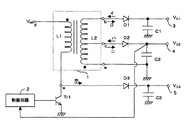
図1に第1の実施形態で使用するDC/DCコンバータの内部構成を示す。該DC/DCコンバータは、1次側コイルL1と2次側コイルL2で構成されたトランス1を有している。直流電圧が入力される1次側コイルL1にはNPN型トランジスタTr1のコレクタが接続している。該トランジスタTr1はベースに制御回路2が接続されるとともに、エミッタが接地されている。また、トランジスタTr1のコレクタにダイオードD3が接続し、更に、該ダイオードD3に出力端子5及び他端が接地されたコンデンサC3が接続される。
【0018】
2次側コイルL2は、接点b、cに、それぞれダイオードD1、D2が接続されるとともに、接点aが接地されている。また、ダイオードD1、D2は出力端子3、4に接続し、更に、それぞれ他端が接地されたコンデンサC1、C2と接続している。このようなDC/DCコンバータにおいて、出力端子4の出力信号が制御回路2にフィードバックされる。該制御回路2によって、前記出力信号に応じてトランジスタTr1のON/OFFのタイミング時間TONとTOFFを制御する。
【0019】
尚、前記ダイオードD1、D2、D3は、それぞれトランス1から出力端子3、4、5に向かって電流が流れるように接続されている。
【0020】
図3及び図4を用いて、本実施形態で使用するDC/DCコンバータの動作について説明する。図3は、該DC/DCコンバータの制御回路2のトランジスタTr1への入力信号波形とトランス1の接点b、c、eにおける電圧の変化を表している。又、図4は該DC/DCコンバータのTON及びTOFF時の等価回路を表す。
【0021】
制御回路2によって、図3(a)のような信号がトランジスタTr1のベースに与えられたとき、トランジスタTr1は、TONの間動作するとともに、TOFFの間停止している。また、1次側コイルL1の接点dには直流電圧VINが印加されるものとする。
【0022】
上記のように、トランジスタTr1が動作するとき、TONの間、図4(a)のように、1次側コイルL1に直接VINが印加された状態となるので、1次側コイルL1にエネルギーが蓄えられる。また、接点eが接地された状態となるので、接点eの電圧はLowとなる。更に、2次側コイルL2に逆方向の電圧がかかるため、b点及びc点の電圧はLowとなる。この逆方向の電圧によりイ及びハの方向に流れようとする電流は、ダイオードD1及びD2によって遮断される。
【0023】
TOFFのとき、トランジスタの動作が停止するとともに、ダイオードD1、D2、及びD3が作動し、図4(b)のように、2次側コイルL2の接点b、cに、それぞれ負荷Z1、Z2が接続するとともに、1次側コイルL1の接点eに負荷Z3が接続した状態となるので、TONの間に1次側コイルL1で蓄えられたエネルギーが放出される。コイルに蓄えられたエネルギーは、該コイルに接続した負荷Z1、Z2及びZ3に電圧として供給される。このとき、接点b、c、eから、それぞれロ、ニ、ホの方向に電流が流れ、また、接点b、c、eには、それぞれ出力直流電圧VO1、VO2、VO3がかかる。そのため、接点b、c、eの電圧はそれぞれHiとなる。また、このときトランジスタTr1のコレクタ・エミッタ間にかかる耐電圧VCEは、VO1となる。
【0024】
上記のような動作が繰り返されるため、接点b、c、eでの電圧の変化は図3(b)、(c)、(d)のようになる。このとき、図3(b)及び図3(c)のように変化する電圧において負の電圧となって表れる電圧が、それぞれダイオードD1及びD2によって図3(e)及び図3(f)のようにカットオフされる。また、接点b、c、eでの電圧は、それぞれダイオードD1、D2、D3及びコンデンサC1、C2、C3によって、整流され、直流電圧電源として、出力端子3、4、5より出力される。
【0025】
更に、上記のような動作を示すDC/DCコンバータの出力端子5に、抵抗R1を接続し、該抵抗R1の他端を出力端子6とするとともに、該出力端子6に接地されたツェナーダイオードDT1と接地されたコンデンサーC5とが並列に接続された安定化回路を図5(a)に示す。尚、ツェナーダイオードDT1は、接地側から出力端子6側に順バイアスがかかるように接続されている。
【0026】
このとき、ツェナーダイオードDT1にかかる逆バイアスが、ある一定の大きさの電圧を提供するので、出力端子5と出力端子6の間の回路が安定化回路7として動作するため、出力端子5から出力される直流電圧はより安定化された直流電圧として、出力端子6より出力される。
【0027】
図5(b)は、図5(a)とは別の安定化回路7を接続した例である。前記DC/DCコンバータの出力端子5に、NPN型トランジスタTr3のコレクタが接続し、該トランジスタTr3のコレクタ・ベース間に抵抗R2が接続されている。また、該トランジスタTr3のエミッタには、他端が接地されたコンデンサC6と出力端子6が接続するとともに、該トランジスタTr3のベースには、他端が接地されたツェナーダイオードDT2が接続されている。尚、ツェナーダイオードDT2は、接地側からトランジスタTr3のベース側に順バイアスがかかるように接続されている。
【0028】
このような構成の安定化回路7が出力端子5に接続されているとき、ツェナーダイオードDT2にかかる逆バイアスが一定となるので、トランジスタTr3のベース電圧が一定として、該トランジスタTr3のベース・エミッタ間の電圧を調整することができる。そのため、より安定した直流電圧を出力として、出力端子6より得ることができる。
【0029】
図5(c)は、図5(a)及び図5(b)とは別の安定化回路7を接続した例である。前記DC/DCコンバータの出力端子5に、3端子レギュレータ8の入力用端子を接続し、該3端子レギュレータの接地用端子を接地する。また、該3端子レギュレータの出力用端子には、他端が接地されたコンデンサーC7と出力端子6が接続されている。このように、安定化回路である3端子レギュレータ8を接続することによって、出力端子5より出力される直流電圧を更に安定化した直流電圧が、出力端子6より得られる。
【0030】
図2に第2の実施形態で使用するDC/DCコンバータの内部構成を示す。該DC/DCコンバータは、1次側コイルL1と2次側コイルL2で構成されたトランス1を有している。直流電圧が入力される1次側コイルL1にはPNP型トランジスタTr2のコレクタが接続しており、該1次側コイルL1の他点は接地されている。該トランジスタTr2はベースに制御回路2が接続されるとともに、エミッタには直流電圧VINがかかっている。また、トランジスタTr2のコレクタにダイオードD4が接続し、更に、該ダイオードD4に出力端子5及び他端が接地されたコンデンサC4が接続される。
【0031】
2次側コイルL2は、接点b、cに、それぞれダイオードD1、D2が接続されるとともに、接点aが接地されている。また、ダイオードD1、D2は出力端子3、4に接続し、更に、それぞれ他端が接地されたコンデンサC1、C2と接続している。このようなDC/DCコンバータにおいて、出力端子4の出力信号が制御回路2にフィードバックされる。該制御回路2によって、前記出力信号に応じてトランジスタTr2のON/OFFのタイミング時間TONとTOFFを制御する。
【0032】
尚、前記ダイオードD1、D2は、それぞれトランス1から出力端子3、4に向かって電流が流れるように接続され、また、前記ダイオードD4は出力端子5からトランス1に向かって電流が流れるように接続されている。
【0033】
図6及び図7を用いて、本実施形態で使用するDC/DCコンバータの動作について説明する。図6は、該DC/DCコンバータの制御回路2のトランジスタTr2への入力信号波形とトランス1の接点b、c、fにおける電圧の変化を表している。又、図7は該DC/DCコンバータのTON及びTOFF時の等価回路を表す。
【0034】
制御回路2によって、図6(a)のような信号がトランジスタTr2のベースに与えられたとき、トランジスタTr2は、TONの間動作するとともに、TOFFの間停止している。また、トランジスタTr2のエミッタには直流電圧VINが印加されるものとする。
【0035】
上記のように、トランジスタTr2が動作するとき、TONの間、図7(a)のように、1次側コイルL1に直接VINが印加された状態となるので、1次側コイルL1にエネルギーが蓄えられる。また、f点には電圧VINがかかった状態となるので、f点の電圧はHiとなる。このとき、ヘの方向に流れようとする電流は、ダイオードD4によって遮断される。更に、2次側コイルL2に逆方向の電圧がかかるため、接点b及びcの電圧はLowとなり、この逆方向の電圧のためにイ及びハの方向に流れようとする電流が、ダイオードD1及びD2によって遮断される。
【0036】
TOFFのとき、トランジスタの動作が停止するとともに、ダイオードD1、D2、及びD4が作動し、図7(b)のように2次側コイルL2の接点b、cに、それぞれ負荷Z1、Z2が接続するとともに、1次側コイルL1の接点fに負荷Z4が接続した状態となるので、TONの間に1次側コイルL1で蓄えられたエネルギーが放出される。コイルに蓄えられたエネルギーは、該コイルに接続した負荷Z1、Z2及びZ4に電圧として供給される。このとき、接点b、c、fからロ、ニ、トの方向に電流が流れ、また、接点b、c、fには、それぞれ出力直流電圧V04、V05、−V06がかかる。そのため、接点b及び接点cの電圧はそれぞれHiとなり、接点fの電圧はLowとなる。また、このときトランジスタTr2のコレクタ・エミッタ間にかかる耐電圧VCEは、VIN+V06となる。
【0037】
上記のような動作が繰り返されるため、接点b、c、fでの電圧の変化は図6(b)、(c)、(d)のようになる。このとき、図6(b)及び図6(c)のように変化する電圧において負の電圧となって表れる電圧が、それぞれダイオードD1及びD2によって図6(e)及び図6(f)のようにカットオフされ、図6(d)のように変化する電圧において正の電圧となって表れる電圧が、ダイオードD4によって図6(g)のようにカットオフされる。また、接点b、c、fでの電圧は、それぞれダイオードD1、D2、D4及びコンデンサC1、C2、C4によって、整流され、直流電圧電源として、出力端子3、4、5より出力される。
【0038】
【発明の効果】
本発明のDC/DCコンバータによると、1次側のコイルに表れるパルス電流を整流して、直流電源の出力として利用するので、従来のDC/DCコンバータのトランスの大きさを変更することなく、その出力を1つ増加することができる。
【0039】
本発明のDC/DCコンバータによると、トランスの大きさを変更することなく、同じ大きさのトランスを使用した従来のDC/DCコンバータの出力に1出力を増加したDC/DCコンバータとなるので、同じ数の出力を持った従来のDC/DCコンバータよりもその規模が小さくなり、且つ、コストダウンをはかることができる。
【0040】
本発明のDC/DCコンバータによると、1次側のコイルに接続したトランジスタのエミッタ・コレクタ間に負荷が接続された状態となるために、無負荷時に比べて停止時の該トランジスタのエミッタ・コレクタ間にかかる耐電圧が低くなり、従来のDC/DCコンバータに使用されるトランジスタよりもコレクタ・エミッタ間の耐電圧が低いトランジスタを使用することができるので、コストダウンをはかれる。
【0041】
本発明のDC/DCコンバータによると、1次側にかかるパルス電圧を整流する整流回路に安定化回路を接続することによって、より安定した出力の直流電圧が得られる。
【図面の簡単な説明】
【図1】第1の実施形態で使用するDC/DCコンバータの回路図。
【図2】第2の実施形態で使用するDC/DCコンバータの回路図。
【図3】第1の実施形態で使用するDC/DCコンバータの制御回路の入力信号波形と接点b、c、eの電圧波形。
【図4】第1の実施形態で使用するDC/DCコンバータのTON及びTOFF時の等価回路図。
【図5】本発明で使用するDC/DCコンバータの出力端子5に接続する安定化回路の回路図。
【図6】第2の実施形態で使用するDC/DCコンバータの制御回路の入力信号波形と接点b、c、fの電圧波形。
【図7】第2の実施形態で使用するDC/DCコンバータのTON及びTOFF時の等価回路図。
【図8】出力端子が1つである従来のDC/DCコンバータの回路図。
【図9】出力端子が2つである従来のDC/DCコンバータの回路図。
【符号の説明】
1 トランス
2 制御回路
3〜6 出力端子
7 安定化回路
8 3端子レギュレータ
C1〜C7 コンデンサ
D1〜D4 ダイオード
DT1,DT2 ツェナーダイオード
L1 1次側コイル
L2 2次側コイル
R1,R2 抵抗
Tr1,Tr3 NPN型トランジスタ
Tr2 PNP型トランジスタ[0001]
BACKGROUND OF THE INVENTION
The present invention relates to a DC / DC converter having a transformer inside, and particularly to a DC / DC converter that requires a plurality of outputs.
[0002]
[Prior art]
8 and 9 show the internal configuration of a DC / DC converter conventionally used. FIG. 8 shows a DC / DC converter with one output. The DC / DC converter has a
[0003]
The diode D1 is connected so that a current flows from the
[0004]
In the DC / DC converter having such a configuration, when a DC voltage is input to the primary coil L1, the
[0005]
By performing such an operation, since the current value of the primary coil L1 changes, the primary coil L1 is excited to generate a magnetic field, and the secondary coil L2 is excited by the generated magnetic field. Is done. In this way, the secondary coil L2 is mutually induced by the primary coil L1, and a pulse voltage is applied to the secondary side. The pulse voltage generated in this way is rectified by the diode D1 and the capacitor C1, and output as a DC power supply. The DC voltage output at this time is determined by the winding ratio of the coils L1 and L2 and the voltage on the input side.
[0006]
FIG. 9 shows a configuration diagram of a DC / DC converter in which the output of the DC / DC converter as described above is increased by one and the output voltage becomes two. In the DC / DC converter, the output shown in FIG. 8 is connected to the contact c of the secondary side coil L2 of one DC / DC converter through a diode D2 and connected to a capacitor C2 whose other end is grounded. The output terminal 4 is connected. At this time, the output signal fed back to the
[0007]
The operation of the DC / DC converter having such a configuration is the same as that of the DC / DC converter having one output terminal shown in FIG. Therefore, the secondary coil L2 is mutually induced by the primary coil L1, and a pulse voltage is applied to the contacts b and c of the coil L2. The pulse voltages generated in this way are rectified by the diodes D1 and D2 and the capacitors C1 and C2, respectively, and output as DC power from the output terminals 3 and 4. In addition, the DC voltage output at the output terminals 3 and 4 at this time is the winding between the primary side coil and the secondary side coil ab, respectively, in addition to the voltage value of the DC voltage input to the primary side coil. The line ratio is determined by the winding ratio between the primary side coil and the secondary side coil ac.
[0008]
The diodes D1 and D2 are connected so that a current flows from the
[0009]
[Problems to be solved by the invention]
Conventionally used DC / DC converters increase the output serving as a DC power source by increasing the number of output terminals connected to the secondary coil L2 in the
[0010]
[Means for Solving the Problems]
In order to achieve the above object, in the DC / DC converter of the present invention , the current flowing through the primary side coil is intermittently switched by the switching element to obtain the pulse voltage in the secondary side coil . A first circuit rectified by a first diode and a first capacitor and output as a first DC voltage power supply; and a pulse voltage generated in the primary coil is rectified by a second diode and a second capacitor. And a second circuit for outputting as a second DC voltage source, and one end of a resistor is further connected to the output side of the second circuit, and a Zener diode is connected between the other end of the resistor and the ground. The voltage is output from a connection point between the resistor and the Zener diode .
[0011]
An object of the present invention is to provide a DC / DC converter capable of increasing an output serving as a DC power source without changing a transformer provided in a conventional DC / DC converter.
[0012]
Another object of the present invention is to provide a DC / DC converter that can increase the output serving as a DC power supply at low cost and without increasing the shape.
[0013]
[Means for Solving the Problems]
The DC / DC converter according to
[0014]
By connecting a rectifier circuit to the connection between the coil on the primary side of the transformer and the switching element to obtain a DC voltage power supply, the DC current is one more than that of a conventional DC / DC converter using the same transformer. Acquire voltage power supply.
[0015]
By using a transistor as the switching element and connecting a control circuit for controlling the ON / OFF of the transistor by feeding back the output of the secondary coil to the base of the transistor, the output of the secondary coil Keep constant.
[0016]
Furthermore, a resistor is connected to the output side of the rectifier circuit that rectifies the pulse voltage generated in the primary coil, and a Zener diode and a capacitor are connected in parallel between the resistor and the ground.
A transistor collector is connected to the output side of the rectifier circuit, a resistor is connected between the base and collector of the transistor, a Zener diode is connected between the base of the transistor and ground, and a capacitor is connected between the emitter and ground. Or connect
Further, the input terminal of the three-terminal regulator is connected to the output side of the rectifier circuit, the ground terminal of the three-terminal regulator is grounded, and a capacitor is connected between the output terminal of the three-terminal regulator and the ground. ,
A stabilization circuit is connected between the output side of the rectifier circuit and the output of the DC voltage power supply to stabilize the output.
[0017]
DETAILED DESCRIPTION OF THE INVENTION
FIG. 1 shows the internal configuration of the DC / DC converter used in the first embodiment. The DC / DC converter has a
[0018]
In the secondary coil L2, the diodes D1 and D2 are connected to the contacts b and c, respectively, and the contact a is grounded. The diodes D1 and D2 are connected to the output terminals 3 and 4 and are further connected to capacitors C1 and C2 whose other ends are grounded. In such a DC / DC converter, the output signal of the output terminal 4 is fed back to the
[0019]
The diodes D1, D2, and D3 are connected so that current flows from the
[0020]
The operation of the DC / DC converter used in this embodiment will be described with reference to FIGS. FIG. 3 shows the waveform of the input signal to the transistor Tr1 of the
[0021]
When a signal as shown in FIG. 3A is given to the base of the transistor Tr1 by the
[0022]
As described above, when the transistor Tr1 operates, during T ON , as shown in FIG. 4A, V IN is directly applied to the primary side coil L1, so that the primary side coil L1 Energy is stored. Further, since the contact point e is grounded, the voltage at the contact point e is Low. Further, since a reverse voltage is applied to the secondary coil L2, the voltages at the points b and c are Low. Currents that flow in the directions of A and C due to the reverse voltage are blocked by the diodes D1 and D2.
[0023]
When T OFF , the operation of the transistor is stopped and the diodes D1, D2, and D3 are activated, and the loads Z1, Z2 are respectively applied to the contacts b, c of the secondary coil L2, as shown in FIG. 4B. There as well as connections, the load Z3 to contact e of the primary coil L1 is in a state of being connected, the energy stored in the primary coil L1 during T oN is emitted. The energy stored in the coil is supplied as a voltage to loads Z1, Z2, and Z3 connected to the coil. At this time, current flows from the contacts b, c, and e in the directions of B, D, and E, respectively, and output DC voltages V O1 , V O2 , and V O3 are applied to the contacts b, c, and e, respectively. Therefore, the voltages of the contacts b, c, e are Hi. At this time, the withstand voltage V CE applied between the collector and the emitter of the transistor Tr1 is V O1 .
[0024]
Since the above operation is repeated, the voltage changes at the contacts b, c, e are as shown in FIGS. 3B, 3C, and 3D. At this time, the voltages appearing as negative voltages in the voltage changing as shown in FIG. 3B and FIG. 3C are respectively shown in FIG. 3E and FIG. 3F by the diodes D1 and D2. Will be cut off. The voltages at the contacts b, c, e are rectified by the diodes D1, D2, D3 and the capacitors C1, C2, C3, respectively, and output from the
[0025]
Further, the resistor R1 is connected to the
[0026]
At this time, since the reverse bias applied to the Zener diode D T1 provides a certain voltage, the circuit between the
[0027]
FIG. 5B shows an example in which a stabilization circuit 7 different from that shown in FIG. The collector of an NPN transistor Tr3 is connected to the
[0028]
When the stabilization circuit 7 having such a configuration is connected to the
[0029]
FIG. 5C shows an example in which a stabilization circuit 7 different from those shown in FIGS. 5A and 5B is connected. The input terminal of the three-terminal regulator 8 is connected to the
[0030]
FIG. 2 shows the internal configuration of the DC / DC converter used in the second embodiment. The DC / DC converter has a
[0031]
In the secondary coil L2, the diodes D1 and D2 are connected to the contacts b and c, respectively, and the contact a is grounded. The diodes D1 and D2 are connected to the output terminals 3 and 4 and are further connected to capacitors C1 and C2 whose other ends are grounded. In such a DC / DC converter, the output signal of the output terminal 4 is fed back to the
[0032]
The diodes D1 and D2 are connected so that current flows from the
[0033]
The operation of the DC / DC converter used in this embodiment will be described with reference to FIGS. FIG. 6 shows the waveform of the input signal to the transistor Tr2 of the
[0034]
When a signal as shown in FIG. 6A is given to the base of the transistor Tr2 by the
[0035]
As described above, when the transistor Tr2 operates, during T ON , as shown in FIG. 7A, V IN is directly applied to the primary side coil L1, so that the primary side coil L1 Energy is stored. Further, since the voltage V IN is applied to the point f, the voltage at the point f becomes Hi. At this time, the current that tends to flow in the direction of F is blocked by the diode D4. Further, since a reverse voltage is applied to the secondary coil L2, the voltages at the contacts b and c become Low, and the current that flows in the directions A and C due to the reverse voltage is applied to the diodes D1 and D2. Blocked by D2.
[0036]
When T OFF , the operation of the transistor is stopped and the diodes D1, D2, and D4 are activated, and the loads Z1 and Z2 are respectively connected to the contacts b and c of the secondary coil L2 as shown in FIG. 7B. while connected, a state in which the load Z4 is connected to the contact f of the primary coil L1, the energy stored in the primary coil L1 during T oN is emitted. The energy stored in the coil is supplied as a voltage to loads Z1, Z2 and Z4 connected to the coil. At this time, current flows from the contacts b, c, and f in the direction of B, D, and G, and output DC voltages V 04 , V 05 , and −V 06 are applied to the contacts b, c, and f, respectively. Therefore, the voltage at the contact point b and the contact point c is Hi, and the voltage at the contact point f is Low. At this time, the withstand voltage V CE applied between the collector and emitter of the transistor Tr2 is V IN + V 06 .
[0037]
Since the operation as described above is repeated, the voltage changes at the contacts b, c, and f are as shown in FIGS. 6B, 6C, and 6D. At this time, the voltages appearing as negative voltages in the voltage changing as shown in FIGS. 6B and 6C are respectively shown in FIGS. 6E and 6F by the diodes D1 and D2. The voltage that appears as a positive voltage in the voltage that changes as shown in FIG. 6D is cut off as shown in FIG. 6G by the diode D4. The voltages at the contacts b, c, and f are rectified by the diodes D1, D2, and D4 and the capacitors C1, C2, and C4, respectively, and output from the
[0038]
【The invention's effect】
According to the DC / DC converter of the present invention, since the pulse current appearing in the primary side coil is rectified and used as the output of the DC power supply, without changing the size of the transformer of the conventional DC / DC converter, Its output can be increased by one.
[0039]
According to the DC / DC converter of the present invention, it becomes a DC / DC converter in which one output is increased to the output of a conventional DC / DC converter using a transformer of the same size without changing the size of the transformer. The scale is smaller than that of a conventional DC / DC converter having the same number of outputs, and the cost can be reduced.
[0040]
According to the DC / DC converter of the present invention, since the load is connected between the emitter and collector of the transistor connected to the primary side coil, the emitter and collector of the transistor at the time of stop compared to the case of no load. Since the withstand voltage applied between them is low and a transistor having a withstand voltage between the collector and the emitter lower than that of the transistor used in the conventional DC / DC converter can be used, the cost can be reduced.
[0041]
According to the DC / DC converter of the present invention, a more stable output DC voltage can be obtained by connecting a stabilization circuit to a rectifier circuit that rectifies the pulse voltage applied to the primary side.
[Brief description of the drawings]
FIG. 1 is a circuit diagram of a DC / DC converter used in a first embodiment.
FIG. 2 is a circuit diagram of a DC / DC converter used in the second embodiment.
FIG. 3 shows an input signal waveform of a DC / DC converter control circuit used in the first embodiment and voltage waveforms of contacts b, c and e.
FIG. 4 is an equivalent circuit diagram at the time of T ON and T OFF of the DC / DC converter used in the first embodiment.
FIG. 5 is a circuit diagram of a stabilization circuit connected to an
FIG. 6 shows an input signal waveform of a DC / DC converter control circuit used in the second embodiment and voltage waveforms of contacts b, c, and f.
FIG. 7 is an equivalent circuit diagram at the time of T ON and T OFF of the DC / DC converter used in the second embodiment.
FIG. 8 is a circuit diagram of a conventional DC / DC converter having one output terminal.
FIG. 9 is a circuit diagram of a conventional DC / DC converter having two output terminals.
[Explanation of symbols]
DESCRIPTION OF
Claims (1)
Priority Applications (1)
| Application Number | Priority Date | Filing Date | Title |
|---|---|---|---|
| JP23061298A JP3732012B2 (en) | 1998-08-17 | 1998-08-17 | DC / DC converter using primary winding of transformer |
Applications Claiming Priority (1)
| Application Number | Priority Date | Filing Date | Title |
|---|---|---|---|
| JP23061298A JP3732012B2 (en) | 1998-08-17 | 1998-08-17 | DC / DC converter using primary winding of transformer |
Publications (2)
| Publication Number | Publication Date |
|---|---|
| JP2000060123A JP2000060123A (en) | 2000-02-25 |
| JP3732012B2 true JP3732012B2 (en) | 2006-01-05 |
Family
ID=16910500
Family Applications (1)
| Application Number | Title | Priority Date | Filing Date |
|---|---|---|---|
| JP23061298A Expired - Fee Related JP3732012B2 (en) | 1998-08-17 | 1998-08-17 | DC / DC converter using primary winding of transformer |
Country Status (1)
| Country | Link |
|---|---|
| JP (1) | JP3732012B2 (en) |
Families Citing this family (1)
| Publication number | Priority date | Publication date | Assignee | Title |
|---|---|---|---|---|
| KR101710537B1 (en) * | 2015-07-09 | 2017-03-13 | 숭실대학교산학협력단 | Coupled-inductor boost-charge pump-flyback converter |
-
1998
- 1998-08-17 JP JP23061298A patent/JP3732012B2/en not_active Expired - Fee Related
Also Published As
| Publication number | Publication date |
|---|---|
| JP2000060123A (en) | 2000-02-25 |
Similar Documents
| Publication | Publication Date | Title |
|---|---|---|
| US8467201B2 (en) | Simplified primary triggering circuit for the switch in a switched-mode power supply | |
| JPH11122926A (en) | Self-oscillating switching power supply | |
| KR920008204B1 (en) | Switching controlled power circuit | |
| US4460955A (en) | Stabilizing power supply apparatus | |
| JP2000060123A (en) | Dc-to-dc converter using primary winding of transformer | |
| JP3447975B2 (en) | Switching power supply circuit | |
| US4176302A (en) | Vertical deflection output circuit | |
| US6188207B1 (en) | Switching power supply | |
| JP3475415B2 (en) | DC-DC converter | |
| JPH0315423B2 (en) | ||
| JP3500868B2 (en) | Switching regulator | |
| JP3427088B2 (en) | Switching power supply | |
| JPH0740720B2 (en) | Switching power supply for multi-scan television receiver | |
| JP2563188B2 (en) | Self-exciting converter with overcurrent protection | |
| JP2986979B2 (en) | Multi-output type switching power supply | |
| JPH11341805A (en) | Stabilized power supply circuit | |
| JP2000324814A (en) | Switching power supply | |
| JPH0231913Y2 (en) | ||
| JPH0756635Y2 (en) | Self-excited switching power supply circuit | |
| JP3468092B2 (en) | Switching power supply | |
| JPS6316311Y2 (en) | ||
| JPS6244367Y2 (en) | ||
| JP2006109543A (en) | Dc-dc converter | |
| JPS6223544B2 (en) | ||
| JPH01114370A (en) | switching power supply |
Legal Events
| Date | Code | Title | Description |
|---|---|---|---|
| A621 | Written request for application examination |
Free format text: JAPANESE INTERMEDIATE CODE: A621 Effective date: 20031216 |
|
| A977 | Report on retrieval |
Free format text: JAPANESE INTERMEDIATE CODE: A971007 Effective date: 20050224 |
|
| A131 | Notification of reasons for refusal |
Free format text: JAPANESE INTERMEDIATE CODE: A131 Effective date: 20050308 |
|
| A521 | Written amendment |
Free format text: JAPANESE INTERMEDIATE CODE: A523 Effective date: 20050509 |
|
| TRDD | Decision of grant or rejection written | ||
| A01 | Written decision to grant a patent or to grant a registration (utility model) |
Free format text: JAPANESE INTERMEDIATE CODE: A01 Effective date: 20051011 |
|
| A61 | First payment of annual fees (during grant procedure) |
Free format text: JAPANESE INTERMEDIATE CODE: A61 Effective date: 20051011 |
|
| R150 | Certificate of patent or registration of utility model |
Free format text: JAPANESE INTERMEDIATE CODE: R150 |
|
| FPAY | Renewal fee payment (event date is renewal date of database) |
Free format text: PAYMENT UNTIL: 20111021 Year of fee payment: 6 |
|
| LAPS | Cancellation because of no payment of annual fees |