JP3824497B2 - Light emitting element array - Google Patents
Light emitting element array Download PDFInfo
- Publication number
- JP3824497B2 JP3824497B2 JP2001119581A JP2001119581A JP3824497B2 JP 3824497 B2 JP3824497 B2 JP 3824497B2 JP 2001119581 A JP2001119581 A JP 2001119581A JP 2001119581 A JP2001119581 A JP 2001119581A JP 3824497 B2 JP3824497 B2 JP 3824497B2
- Authority
- JP
- Japan
- Prior art keywords
- wiring
- cell
- light emitting
- electrically connected
- electrode pad
- Prior art date
- Legal status (The legal status is an assumption and is not a legal conclusion. Google has not performed a legal analysis and makes no representation as to the accuracy of the status listed.)
- Expired - Lifetime
Links
Images


Classifications
-
- G—PHYSICS
- G09—EDUCATION; CRYPTOGRAPHY; DISPLAY; ADVERTISING; SEALS
- G09G—ARRANGEMENTS OR CIRCUITS FOR CONTROL OF INDICATING DEVICES USING STATIC MEANS TO PRESENT VARIABLE INFORMATION
- G09G3/00—Control arrangements or circuits, of interest only in connection with visual indicators other than cathode-ray tubes
- G09G3/04—Control arrangements or circuits, of interest only in connection with visual indicators other than cathode-ray tubes for presentation of a single character by selection from a plurality of characters, or by composing the character by combination of individual elements, e.g. segments using a combination of such display devices for composing words, rows or the like, in a frame with fixed character positions
- G09G3/06—Control arrangements or circuits, of interest only in connection with visual indicators other than cathode-ray tubes for presentation of a single character by selection from a plurality of characters, or by composing the character by combination of individual elements, e.g. segments using a combination of such display devices for composing words, rows or the like, in a frame with fixed character positions using controlled light sources
- G09G3/12—Control arrangements or circuits, of interest only in connection with visual indicators other than cathode-ray tubes for presentation of a single character by selection from a plurality of characters, or by composing the character by combination of individual elements, e.g. segments using a combination of such display devices for composing words, rows or the like, in a frame with fixed character positions using controlled light sources using electroluminescent elements
- G09G3/14—Semiconductor devices, e.g. diodes
-
- B—PERFORMING OPERATIONS; TRANSPORTING
- B41—PRINTING; LINING MACHINES; TYPEWRITERS; STAMPS
- B41J—TYPEWRITERS; SELECTIVE PRINTING MECHANISMS, i.e. MECHANISMS PRINTING OTHERWISE THAN FROM A FORME; CORRECTION OF TYPOGRAPHICAL ERRORS
- B41J2/00—Typewriters or selective printing mechanisms characterised by the printing or marking process for which they are designed
- B41J2/435—Typewriters or selective printing mechanisms characterised by the printing or marking process for which they are designed characterised by selective application of radiation to a printing material or impression-transfer material
- B41J2/447—Typewriters or selective printing mechanisms characterised by the printing or marking process for which they are designed characterised by selective application of radiation to a printing material or impression-transfer material using arrays of radiation sources
- B41J2/45—Typewriters or selective printing mechanisms characterised by the printing or marking process for which they are designed characterised by selective application of radiation to a printing material or impression-transfer material using arrays of radiation sources using light-emitting diode [LED] or laser arrays
-
- H—ELECTRICITY
- H10—SEMICONDUCTOR DEVICES; ELECTRIC SOLID-STATE DEVICES NOT OTHERWISE PROVIDED FOR
- H10H—INORGANIC LIGHT-EMITTING SEMICONDUCTOR DEVICES HAVING POTENTIAL BARRIERS
- H10H29/00—Integrated devices, or assemblies of multiple devices, comprising at least one light-emitting semiconductor element covered by group H10H20/00
- H10H29/10—Integrated devices comprising at least one light-emitting semiconductor component covered by group H10H20/00
- H10H29/14—Integrated devices comprising at least one light-emitting semiconductor component covered by group H10H20/00 comprising multiple light-emitting semiconductor components
Landscapes
- Physics & Mathematics (AREA)
- Engineering & Computer Science (AREA)
- Optics & Photonics (AREA)
- Health & Medical Sciences (AREA)
- General Health & Medical Sciences (AREA)
- Toxicology (AREA)
- Computer Hardware Design (AREA)
- General Physics & Mathematics (AREA)
- Theoretical Computer Science (AREA)
- Led Devices (AREA)
- Led Device Packages (AREA)
- Printers Or Recording Devices Using Electromagnetic And Radiation Means (AREA)
Description
【0001】
【発明の属する技術分野】
この発明は、いわゆる多層配線構造を有する発光素子アレイに関するものである。
【0002】
【従来の技術】
発光素子アレイは、複数の発光素子を直線状に配置したものである。発光素子としてLED(light emitting diode;発光ダイオード)を採用したものがLEDアレイである。LEDアレイは、例えば、電子写真プリンタの露光光源として使用されている。
【0003】
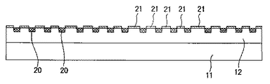
LEDアレイとしては、例えば、「LEDプリンタの設計」トリケップス社の第60頁に開示されている(図17および図18)。図17は、従来のLEDアレイの断面図である。図18は、従来のLEDアレイの上面図である。
【0004】
図17および図18に示されるように、このLEDアレイは、n型GaAs基板1上にn型GaAs0.6P0.4層2を形成し、Zn等のp型不純物の選択拡散により複数の発光部3をアレイ状に配置する。各発光部3のそれぞれのAl電極(個別電極)4は、それぞれの発光部3に電気的に接続されるように絶縁層6を挟んでp型GaAs0.6P0.4層3上に形成される。これらのAl電極4は、それぞれのワイヤボンド電極部(以下、電極パッドいう)7に電気的に接続されている。Au−Ge−Ni電極(共通電極)5は、n型GaAs基板1と電気的に接続されるように、その下方に形成される。
【0005】
図19は、従来の多層配線型LEDアレイのセルを示す図である。図20は、図19に示されるA部の拡大図である。
図19に示される多層配線型LEDアレイは、近年、発明者等により提案されたものであり、電極パッド数の低減を主要目的とし、さらに、発光素子の順方向電圧を小さくし消費電力を低減するとともに、ICチップのサイズを小さくし製造コストを低減することを目的としている。
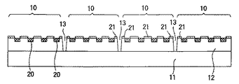
【0006】
図19に示されるように、多層配線型LEDアレイは、LED(発光素子)20に電気的に接続されるp側配線32とp側電極パッド33に電気的に接続される共通配線60とを層間絶縁膜50を介して積層したものである。この多層配線型LEDアレイでは、p側配線32と共通配線60とが直交するように形成されるとともに、LED(発光素子)20を構成する半導体層12が相互に分離(アイソレート)され、複数のブロック10に分割されている。
【0007】
多層配線型LEDアレイは、例えば、次のような方法により製造することができる。まず、高抵抗基板11上にn型の半導体層12が形成される。次に、素子分離溝13が形成され、半導体層がM個のブロック10に電気的に分離される。次に、拡散マスク21を介して選択的にp型不純物が拡散され、各ブロック毎にN個のLED(p側半導体領域(発光素子))20が形成される。
【0008】
次に、N個のLED20に1対1で接続されるp側電極31と、これらのp側電極31に1対1で接続されるp側配線32と、各ブロック10の1つのp側配線32が接続されるp側電極パッド33とが形成される。次に、拡散マスク21の一部が剥離され、各ブロックのn型の半導体層12に1対1で接続されるn側電極41が形成される。次に、n側電極41に1対1で接続されるn側配線42と、n側配線42に1対1で接続されるn側電極パッド43とが形成される。
【0009】
次に、各p側配線32の所定位置が露出する開口部51が層間絶縁膜50に形成される。次に、N個のブロック10にまたがるようにそれぞれのブロック10の1つのp側配線32に接続されるN個の共通配線60が形成される。
【0010】
この多層配線型LEDアレイによれば、n側電極41をLED(p型不純物拡散領域(発光素子))20に近接させて形成し、高抵抗基板11の抵抗成分による電圧降下の影響を小さくする。これにより、LEDの順方向電圧を小さくし、消費電力を低減することができる。また、ワイヤボンディング用のp側電極パッド33およびn側電極パッド43をセルの片側に配置することにより、チップサイズを小さくし、製造コストを低減することができる。
【0011】
【発明が解決しようとする課題】
しかしながら、従来の多層配線型LEDアレイには、p側電極パッド33とn側電極パッド43とを交互に配置すると、セルの右半分において、p側電極パッド33のp側配線32とn側電極パッド43のn側引出配線42とが重なるように形成されてしまう(図20)。この重なりは、
1)配線不良が発生する要因になる
2)これらを同一材料で構成することができない
3)これらを同一工程で形成することができない
といった問題を生じさせる。
【0012】
この発明は、かかる問題点を解決するためになされたものであり、配線不良の可能性を小さくし、信頼性を向上させるとともに、p側電極パッド、p側配線およびp側電極、並びに、n側電極パッドおよびn側配線を同一材料、同一工程で形成し、工程を簡略化することができる発光素子アレイを提供することにある。
【0013】
【課題を解決するための手段】
請求項1に係る発光素子アレイは、基板上に形成されるセル内の半導体層がエッチングにより形成される素子分離溝により分割される複数のブロックを備え、各ブロックは、選択拡散により半導体層にアレイ状に形成される複数の発光素子と、複数の発光素子のそれぞれに電気的に接続される複数の第1電極と、複数の第1電極のそれぞれに電気的に接続される複数の第1配線と、複数の第1配線のうち1つの第1配線が接続される第1電極パッドと、複数の発光素子に近接するように形成される第2電極と、第2電極に電気的に接続される第2配線と、第2配線に電気的に接続される第2電極パッドとをそれぞれ有し、セル内には、複数のブロックにまたがり形成されるブロック内の発光素子数と同数の共通配線であり、各ブロックそれぞれの1つの第1配線に層間絶縁膜の開口部を通して電気的に接続される複数の共通配線を有する多層配線構造の発光素子アレイにおいて、セル内の複数の第1電極パッドおよび複数の第2電極パッドは、同一ブロック内で前記第1配線と前記第2配線とが交差しないよう、該ブロック内の第1電極パッドと第2電極パッドがセル内の長手方向における中央を境界に対称かつ交互に配置されることを特徴とするものである。
【0014】
請求項2に係る発光素子アレイは、基板上に形成されるセル内の半導体層がエッチングにより形成される素子分離溝により分離される複数のブロックを備え、各ブロックは、選択拡散により半導体層にアレイ状に形成される複数の発光素子と、複数の発光素子のそれぞれに電気的に接続される複数の第1電極と、複数の第1電極のそれぞれに電気的に接続される複数の第1配線と、複数の第1配線のうち1つの第1配線が接続される第1電極パッドと、複数の発光素子に近接するように形成される第2電極と、第2電極の中央部に電気的に接続される第2配線と、第2配線に電気的に接続される第2電極パッドとをそれぞれ有し、セル内には、複数のブロックにまたがり形成されるブロック内の発光素子数と同数の共通配線であり、各ブロックそれぞれの1つの第1配線に層間絶縁膜の開口部を通して電気的に接続される複数の共通配線を有する多層配線構造の発光素子アレイにおいて、セル内の複数の第1電極パッドおよび複数の第2電極パッドは、同一ブロック内で前記第1配線と前記第2配線とが交差しないよう、該ブロック内の第1電極パッドと第2電極パッドがセル内の長手方向における中央を境界に対称かつ交互に配置されることを特徴とするものである。
【0017】
【発明の実施の形態】
以下、本発明に係る発光素子アレイの好ましい実施の形態を図面を参照して説明する。
実施の形態1および2において、多層配線型のLEDアレイを例とし、第1導電型をp型、第2導電型をn型としているが、第1導電型をn型、第2導電型をp型としてもよい。基板、電極、配線、不純物等の材料および組成は、実施の形態1および2のものに限られず、種々のものを採用することができる。
【0018】
発光素子アレイは、LEDアレイに限られず、例えば半導体レーザのような他の発光素子に適用することができる。さらに、例えばドライバICのような他の半導体素子にも適用することができる。
【0019】
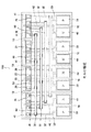
実施の形態1.
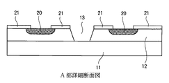
図2は、この発明に係る実施の形態1のLEDアレイの概念図である。図1は、図2に示されるセルの構成を示す図である。図3は、図1に示されるA部断面図である。
【0020】
図2に示されるように、LEDアレイは、その長手方向にリニア状に配置される複数のセル100から構成される多層配線型のLEDアレイである。
【0021】
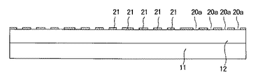
図1および図3に示されるように、この多層配線型のLEDアレイは、高抵抗基板11上に形成される第2導電型半導体層12を備える。高抵抗基板11としては、例えば半絶縁性GaAs基板を用いることができる。第2導電性の半導体層12としては、例えばエピキャピタル成長したn型AlGaAs層を用いることができる。セル100内の第2導電型半導体層12は、エッチングにより形成される素子分離溝13によりM個のブロック10に電気的に分離される。
【0022】
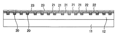
各ブロック10は、第2導電型半導体層12内における不純物の拡散によりpn接合を構成するN個のLED(第1導電型半導体領域(発光素子))20を有する。これらN個のLED20は、セル100の一方の側にセル100の長手方向に1列に配列される。不純物としては、例えばZnを用いることができる。
【0023】
各ブロック10は、1列に配列されるN個のLED20に電気的に接続されるN個のp側電極31と、これらのp側電極31のそれぞれに電気的に接続されるN個のp側配線32と、これらのp側配線32のうち1つのp側配線32と電気的に接続されるp側電極パッド33とを有する。
【0024】
N個のp側電極31は、それぞれのLED20に電気的に接続されるように絶縁膜(拡散マスク)21を挟んで形成される。N個のp側配線32は、セル100内の一方の側から他方の側に、セル100の長手方向と直交する方向に延在する。p側電極パッド33は、セル100内の他方の側に配置される。
【0025】
N個のp側電極31、N個のp側配線32およびp側電極パッド33は、後述するように、同一材料により同時に形成することができる。これらは、一体に形成することができる。これらは、例えばAu積層膜を用いることができる。なお、p側電極パッド33は、N個のp側電極31およびN個のp側配線32と別体として形成されてもよい。
【0026】
各ブロック10は、1つのn側電極41と、n側電極41に電気的に接続されるn側配線42と、n側配線42に電気的に接続されるn側電極パッド43とを有する。n側電極41は、N個のLED20に近接し沿うように、セル100の一方の側のLED20より外側に配置される。n側電極パッド43は、p側電極パッド33と1列に並ぶようにセル100の他方の側に配置されている。n側配線42は、n側電極41とn側電極パッド43とを電気的に接続するように、セル100内の一方の側から他方の側に、セル100の長手方向と直交する方向に延在する。
【0027】
n側電極41は、例えばAu合金膜を用いることができる。n側配線42およびn側電極パッド43は、後述するように、複数のp側電極31、複数のp側配線32およびp側電極パッド33と同一材料により同時に形成することができる。n側配線42およびn側電極パッド43は、一体に形成することができる。
【0028】
n側電極41は、複数のLED20に近接するように配置されるので、高抵抗基板11の抵抗成分による電圧降下の影響を小さくすることができる。したがって、LEDの順方向電圧を小さくし、消費電力を低減することができる。また、p側電極パッド33およびn側電極パッド43をセル100の他方の側に配置することにより、チップサイズを小さくし、製造コストを低減することができる。
【0029】
n側配線42は、n側電極41の中央部に接続されるように形成されるのが好ましい。これにより、図2におけるn側配線42の左右に配列されるN個のLED20とn側配線42との間のそれぞれの距離の差を小さくすることができるので、N個のLEDの発光エネルギ(明るさ)を均一化することができる。
【0030】
セル100内のM個のp側電極パッド33およびM個のn側電極パッド43は、セル100の長手方向における中央を境界に対称かつ交互に1列に配置される。これにより、セル100の中央から右側におけるn側配線42とp側配線32とがn側電極パッド43およびp側電極パッド33の近傍で重ならないように形成することができる。したがって、p側電極31、p側配線32、p側電極パッド33、n側配線42およびn側電極パッド43を同一材料により同時に形成することができる。
【0031】
セル100は、M個のブロック10にまたがるように層間絶縁膜50を介して形成されるN個(ブロック10内のLED20と同数)の共通配線60を有する。N個の共通配線60は、それぞれセル100の長手方向に延在する。N個の共通配線60は、M個のブロック10のそれぞれの1つのp側配線32に電気的に接続される。
【0032】
N個の共通配線60とそれぞれのM個のp側配線32とが交差する位置における層間絶縁膜50には、それぞれの共通配線60およびそれぞれのp側配線32が電気的に接続されるようにコンタクト孔51が形成されている。共通配線60としては、例えばAu積層膜を用いることができる。層間絶縁膜50としては、例えばポリイミド樹脂を用いることができる。
【0033】
M個のブロック10のそれぞれの1つのLED20および対応するp側電極パッド33は、p側電極31およびp側配線32を介して1つのコンタクト孔51を通る共通配線60に電気的に接続される。このため、共通配線60上に2つのコンタクト孔51を設け、一方のコンタクト孔51を通してLED20および共通配線60を電気的に接続し、他方のコンタクト孔51を通して共通配線60およびp側電極パッド33を電気的に接続する場合に比べ、コンタクト孔51の数を少なくすることができる。したがって、LEDアレイの歩留まりを向上させることができる。
【0034】
図4〜図14は、LEDアレイの製造工程を示す図である。図4〜図9は、セル100の断面図であり、図10〜図14は、セル100の上面図である。
【0035】
図4に示されるように、高抵抗基板11上に第2導電型半導体層12が形成され、半導体層12上に拡散マスク21が成膜され、複数のLED20のそれぞれの形成予定領域に開口20aが形成される。拡散マスク21としては、例えばSiN膜を用いることができる。SiN膜は、例えばCVD法により成膜することができる。LED20の形成予定領域の開口20aは、フォトリソグラフィ法またはエッチング法により形成することができる(拡散マスク成膜工程)。
【0036】
次に、図5に示されるように、開口20aを含む拡散マスク21上に拡散源膜22が成膜される。拡散源膜22としては、例えばZnO−SiO2膜を用いることができる。ZnO−SiO2膜は、例えばスパッタ法により成膜することができる(拡散源膜成膜工程)。
【0037】
次に、図6に示されるように、拡散源膜22上にアニールキャップ23が成膜される。アニールキャップ23としては、例えばAlN膜をを用いることができる。AlN膜は、例えばスパッタ法により成膜することができる(アニールキャップ成膜工程)。
【0038】
次に、図7に示されるように、第2導電型半導体層12に第1導電型不純物の拡散領域が選択拡散により形成するためのアニールが行われる。前述のように、第1導電型不純物としては、例えばZnを用いることができる。窒素大気圧下650℃で約3時間アニールすることにより複数のLED形成予定領域である開口20aに拡散領域を形成することができる。これにより、約1μmの拡散深さを有するLED20が形成される(選択拡散アニール工程)。
【0039】
次に、図8に示されるように、アニールキャップ23および拡散源膜22が剥離される。これらの剥離は、選択エッチングにより行うことができる(アニールキャップ/拡散源膜剥離工程)。
【0040】
次に、図9に示されるように、セル100内にその深さが高抵抗基板11に達する(M−1)個の素子分離溝13が形成され、セル100内の第2導電型半導体層12がM個のブロック10に電気的に分離される。素子分離溝13は、例えばリン酸化水をエッチャントとして第2導電型半導体層12を選択的にエッチングすることにより形成することができる(素子分離溝形成工程)。
【0041】
次に、図10に示されるように、後に形成されるn側電極パッド43と第2導電型半導体層12とのコンタクトを取るためにn側電極41の形成予定領域の拡散マスク21が剥離される。剥離は、フォトリソグラフィ法またはエッチング法により行うことができる(拡散マスク剥離工程)。
【0042】
次に、図11に示されるように、n側電極41が成膜される。n側電極41のパターンは、例えばリフトオフ法により形成される(n側電極成膜工程)。
【0043】
次に、図12に示されるように、複数のp側電極31、複数のp側配線32、複数のp側電極パッド33、複数のn側配線42および複数のn側電極パッド43が成膜される。各ブロック10のN個のp側電極31、N個のp側配線32およびp側電極パッド33は一体に成膜され、n側配線42およびn側電極パッド43は一体に成膜される。それぞれのパターンは、例えばリフトオフ法により形成することができる(p側電極等形成工程)。
【0044】
次に、図13に示されるように、層間絶縁膜50が形成される。層間絶縁膜50には、共通配線60のコンタクト孔51となる開口、LED20が形成されている領域の開口およびp側電極パッド33が形成されている領域の開口が形成される。層間絶縁膜50のこれらの開口のパターンは、フォトリソグラフィ法またはエッチング法により形成することができる(層間絶縁膜成膜)。
【0045】
次に、図14に示されるように、セル100内にN個の共通配線60が形成される。1個の共通配線60は、M個のブロック10のそれぞれの1つのLED20に対応するM個のコンタクト孔51を通し、それぞれのp側配線32に電気的に接続される。共通配線60のパターンは、例えばリフトオフ法により形成することができる(共通配線形成工程)。
【0046】
なお、図10〜図12に示される拡散マスク剥離工程、n側電極成膜工程およびp側電極等形成工程の工程順はこれに限るものではない。拡散マスク剥離工程をn側電極成膜工程よりも前に行えばよい。例えば、p側電極等形成工程、拡散マスク剥離工程、n側電極成膜工程の順に行うこともできる。
【0047】
また、p側電極等形成工程を、p側電極31、p側配線32およびp側電極パッド33を形成する工程と、n側配線42およびn側電極パッド43を形成する工程とに分けてもよい。この場合、いずれの工程を先に行ってもよい。
【0048】
実施の形態2.
図15は、この発明に係る実施の形態2のLEDアレイの概念図である。図16は、図15に示されるセルの構成を示す図である。
図15および図16に示されるように、実施の形態2のLEDアレイは、セル200内の複数のp側電極パッド33および複数のn側電極パッド43の配置が実施の形態1のLEDアレイと異なる。
【0049】
実施の形態2のセル200内の複数のp側電極パッド33および複数のn側電極パッド43は、セル200内の長手方向における中央を境界に対称かつ交互に配置される点で実施の形態1と共通する。しかし、実施の形態1の複数のp側電極パッド33および複数のn側電極パッド43は、セル100の長手方向に1列に配置されているのに対し、実施の形態2の複数のp側電極パッド33および複数のn側電極パッド43は、セル200の長手方向に2列に配置されている点が異なる。
【0050】
実施の形態2によれば、複数のp側電極パッド33および複数のn側電極パッド43は、セル200の長手方向に2列に配置されているため、パットサイズを大きくすることができる。したがって、ワイヤボンディングの信頼性を向上させることができる。
【0051】
【発明の効果】
この発明によれば、各ブロック内の第1電極パッドと第2電極パッドとの相対位置を変えることにより、各ブロックの第1配線および引出配線が交差しないように形成することができる。したがって、配線の交差による配線不良を防止し、LEDアレイの信頼性を向上させることができる。また、p側電極パッド、その第1配線およびp側電極、並びに、n側電極パッド及びその引出配線を同一材料、同一工程で形成し、工程を簡略化することができる。
【図面の簡単な説明】
【図1】 図2に示されるセルの構成を示す図である。
【図2】 この発明に係る実施の形態1のLEDアレイの概念図である。
【図3】 図2に示されるA部断面図である。
【図4】 拡散マスク成膜工程を示す図である。
【図5】 拡散源膜成膜工程を示す図である。
【図6】 アニールキャップ成膜工程を示す図である。
【図7】 選択拡散アニール工程を示す図である。
【図8】 アニールキャップ/拡散源膜剥離工程を示す図である。
【図9】 素子分離溝形成工程を示す図である。
【図10】 拡散マスク剥離工程を示す図である。
【図11】 n側電極成膜工程を示す図である。
【図12】 p側電極等形成工程を示す図である。
【図13】 層間絶縁膜成膜工程を示す図である。
【図14】 共通配線形成工程を示す図である。
【図15】 この発明に係る実施の形態2のLEDアレイの概念図である。
【図16】 図15に示されるセルの構成を示す図である。
【図17】 従来のLEDアレイの断面図である。
【図18】 従来のLEDのアレイの上面図である。
【図19】 従来の多層配線型LEDのセルの構成を示す図である。
【図20】 図19に示されるB部拡大図である。
【符号の説明】
10 ブロック
11 高抵抗基板
12 半導体層
13 素子分離溝
20 LED
31 p側電極
32 p側配線
33 p側電極
41 n側電極
42 n側配線
43 n側電極パッド
50 層間絶縁膜
51 コンタクト孔
60 共通配線
100 セル[0001]
BACKGROUND OF THE INVENTION
The present invention relates to a light emitting element array having a so-called multilayer wiring structure.
[0002]
[Prior art]
The light emitting element array is a plurality of light emitting elements arranged in a straight line. An LED array employs an LED (light emitting diode) as a light emitting element. The LED array is used as an exposure light source of an electrophotographic printer, for example.
[0003]
The LED array is disclosed, for example, in “Design of LED Printer” on
[0004]
As shown in FIGS. 17 and 18, this LED array has an n-type GaAs 0.6 P 0.4 layer 2 formed on an n-
[0005]
FIG. 19 is a diagram showing a cell of a conventional multilayer wiring type LED array. 20 is an enlarged view of a portion A shown in FIG.
The multilayer wiring type LED array shown in FIG. 19 has been proposed by the inventors in recent years, and its main purpose is to reduce the number of electrode pads. Further, the forward voltage of the light emitting element is reduced to reduce power consumption. In addition, an object is to reduce the size of the IC chip and reduce the manufacturing cost.
[0006]
As shown in FIG. 19, the multilayer wiring type LED array includes a p-
[0007]
A multilayer wiring type LED array can be manufactured, for example, by the following method. First, the n-
[0008]
Next, a p-
[0009]
Next, an opening 51 in which a predetermined position of each p-
[0010]
According to this multilayer wiring type LED array, the n-
[0011]
[Problems to be solved by the invention]
However, when the p-
1) Cause of wiring failure 2) These cannot be made of the same material 3) The problem that they cannot be formed in the same process is caused.
[0012]
The present invention has been made to solve such a problem. The present invention reduces the possibility of a wiring failure and improves the reliability, as well as the p-side electrode pad, the p-side wiring and the p-side electrode, and n. It is an object of the present invention to provide a light-emitting element array in which side electrode pads and n-side wirings are formed of the same material and in the same process and the process can be simplified.
[0013]
[Means for Solving the Problems]
The light-emitting element array according to
[0014]
The light-emitting element array according to
[0017]
DETAILED DESCRIPTION OF THE INVENTION
Hereinafter, a preferred embodiment of a light-emitting element array according to the present invention will be described with reference to the drawings.
In
[0018]
The light emitting element array is not limited to the LED array, and can be applied to other light emitting elements such as a semiconductor laser. Further, the present invention can be applied to other semiconductor elements such as driver ICs.
[0019]
FIG. 2 is a conceptual diagram of the LED array of
[0020]
As shown in FIG. 2, the LED array is a multilayer wiring type LED array composed of a plurality of
[0021]
As shown in FIGS. 1 and 3, the multilayer wiring type LED array includes a second conductivity
[0022]
Each
[0023]
Each
[0024]
The N p-
[0025]
The N p-
[0026]
Each
[0027]
For the n-
[0028]
Since the n-
[0029]
The n-
[0030]
The M p-
[0031]
The
[0032]
The
[0033]
Each
[0034]
4-14 is a figure which shows the manufacturing process of a LED array. 4 to 9 are cross-sectional views of the
[0035]
As shown in FIG. 4, the second
[0036]
Next, as shown in FIG. 5, a
[0037]
Next, as shown in FIG. 6, an
[0038]
Next, as shown in FIG. 7, annealing is performed to form a diffusion region of the first conductivity type impurity in the second conductivity
[0039]
Next, as shown in FIG. 8, the
[0040]
Next, as shown in FIG. 9, (M−1)
[0041]
Next, as shown in FIG. 10, the
[0042]
Next, as shown in FIG. 11, an n-
[0043]
Next, as shown in FIG. 12, a plurality of p-
[0044]
Next, as shown in FIG. 13, an
[0045]
Next, as shown in FIG. 14, N
[0046]
The order of the diffusion mask peeling process, the n-side electrode film forming process, and the p-side electrode forming process shown in FIGS. 10 to 12 is not limited to this. What is necessary is just to perform a diffusion mask peeling process before an n side electrode film-forming process. For example, a p-side electrode forming process, a diffusion mask peeling process, and an n-side electrode film forming process can be performed in this order.
[0047]
Also, the p-side electrode forming process may be divided into a process of forming the p-
[0048]
FIG. 15 is a conceptual diagram of an LED array according to
As shown in FIGS. 15 and 16, the LED array of the second embodiment is different from the LED array of the first embodiment in the arrangement of the plurality of p-
[0049]
The plurality of p-
[0050]
According to the second embodiment, since the plurality of p-
[0051]
【The invention's effect】
According to the present invention, by changing the relative positions of the first electrode pad and the second electrode pad in each block, the first wiring and the lead wiring in each block can be formed so as not to cross each other. Therefore, it is possible to prevent wiring defects due to wiring intersections and improve the reliability of the LED array. Further, the p-side electrode pad, the first wiring and the p-side electrode, and the n-side electrode pad and the lead-out wiring can be formed with the same material and in the same process, and the process can be simplified.
[Brief description of the drawings]
FIG. 1 is a diagram showing a configuration of a cell shown in FIG.
FIG. 2 is a conceptual diagram of the LED array according to the first embodiment of the present invention.
3 is a cross-sectional view of a portion A shown in FIG.
FIG. 4 is a diagram showing a diffusion mask film forming step.
FIG. 5 is a diagram showing a diffusion source film forming step.
FIG. 6 is a diagram showing an annealing cap film forming step.
FIG. 7 is a diagram showing a selective diffusion annealing step.
FIG. 8 is a diagram showing an annealing cap / diffusion source film peeling step.
FIG. 9 is a diagram showing an element isolation groove forming step.
FIG. 10 is a diagram showing a diffusion mask peeling step.
FIG. 11 is a diagram showing an n-side electrode film forming step.
FIG. 12 is a diagram showing a p-side electrode formation process.
FIG. 13 is a diagram showing a step of forming an interlayer insulating film.
FIG. 14 is a diagram showing a common wiring forming step.
FIG. 15 is a conceptual diagram of an LED array according to a second embodiment of the present invention.
16 is a diagram showing a configuration of the cell shown in FIG.
FIG. 17 is a cross-sectional view of a conventional LED array.
FIG. 18 is a top view of a conventional LED array.
FIG. 19 is a diagram showing a configuration of a cell of a conventional multilayer wiring type LED.
20 is an enlarged view of a portion B shown in FIG.
[Explanation of symbols]
10
31 p-side electrode 32 p-side wiring 33 p-side electrode 41 n-side electrode 42 n-side wiring 43 n-
Claims (6)
各ブロックは、
選択拡散により半導体層にアレイ状に形成される複数の発光素子と、
複数の発光素子のそれぞれに電気的に接続される複数の第1電極と、
複数の第1電極のそれぞれに電気的に接続される複数の第1配線と、
複数の第1配線のうち1つの第1配線が接続される第1電極パッドと、
複数の発光素子に近接するように形成される第2電極と、
第2電極に電気的に接続される第2配線と、
第2配線に電気的に接続される第2電極パッドとをそれぞれ有し、
セル内には、
複数のブロックにまたがり形成されるブロック内の発光素子数と同数の共通配線であり、各ブロックのそれぞれの1つの第1配線に層間絶縁膜の開口部を通して電気的に接続される複数の共通配線を有する多層配線構造の発光素子アレイにおいて、
セル内の複数の第1電極パッドおよび第2電極パッドは、同一ブロック内で前記第1配線と前記第2配線とが交差しないよう、該ブロック内の第1電極パッドと第2電極パッドがセル内の長手方向における中央を境界に対称かつ交互に配置される
ことを特徴とする発光素子アレイ。A plurality of blocks in which a semiconductor layer in a cell formed on a substrate is electrically isolated by an element isolation groove formed by etching;
Each block
A plurality of light emitting elements formed in an array in the semiconductor layer by selective diffusion;
A plurality of first electrodes electrically connected to each of the plurality of light emitting elements;
A plurality of first wirings electrically connected to each of the plurality of first electrodes;
A first electrode pad to which one first wiring among the plurality of first wirings is connected;
A second electrode formed so as to be close to the plurality of light emitting elements;
A second wiring electrically connected to the second electrode;
A second electrode pad electrically connected to the second wiring,
In the cell,
A plurality of common wirings that are as many as the number of light emitting elements in the block formed across the plurality of blocks, and are electrically connected to one first wiring of each block through the opening of the interlayer insulating film In a light-emitting element array having a multilayer wiring structure having
A plurality of first electrode pads and the second electrode pad in the cell, so that the first wiring in the same block and the second wiring do not intersect, the first electrode pad and the second electrode pad in said block cell A light emitting element array, wherein the light emitting element array is arranged symmetrically and alternately with a center in the longitudinal direction as a boundary .
各ブロックは、
選択拡散により半導体層にアレイ状に形成される複数の発光素子と、
複数の発光素子のそれぞれに電気的に接続される複数の第1電極と、
複数の第1電極のそれぞれに電気的に接続される複数の第1配線と、
複数の第1配線のうち1つの第1配線が接続される第1電極パッドと、
複数の発光素子に近接するように形成される第2電極と、
第2電極の中央部に電気的に接続される第2配線と、
第2配線に電気的に接続される第2電極パッドとをそれぞれ有し、
セル内には、
複数のブロックにまたがり形成されるブロック内の発光素子数と同数の共通配線であり、各ブロックのそれぞれの1つの第1配線に層間絶縁膜の開口部を通して電気的に接続される複数の共通配線を有する多層配線構造の発光素子アレイにおいて、
セル内の複数の第1電極パッドおよび第2電極パッドは、同一ブロック内で前記第1配線と前記第2配線とが交差しないよう、該ブロック内の第1電極パッドと第2電極パッドがセル内の長手方向における中央を境界に対称かつ交互に配置される
ことを特徴とする発光素子アレイ。A plurality of blocks in which a semiconductor layer in a cell formed on a substrate is electrically isolated by an element isolation groove formed by etching;
Each block
A plurality of light emitting elements formed in an array in the semiconductor layer by selective diffusion;
A plurality of first electrodes electrically connected to each of the plurality of light emitting elements;
A plurality of first wirings electrically connected to each of the plurality of first electrodes;
A first electrode pad to which one first wiring among the plurality of first wirings is connected;
A second electrode formed so as to be close to the plurality of light emitting elements;
A second wiring electrically connected to the central portion of the second electrode;
A second electrode pad electrically connected to the second wiring,
In the cell,
A plurality of common wirings that are as many as the number of light emitting elements in the block formed across the plurality of blocks, and are electrically connected to one first wiring of each block through the opening of the interlayer insulating film In a light-emitting element array having a multilayer wiring structure having
A plurality of first electrode pads and the second electrode pad in the cell, so that the first wiring in the same block and the second wiring do not intersect, the first electrode pad and the second electrode pad in said block cell A light emitting element array, wherein the light emitting element array is arranged symmetrically and alternately with a center in the longitudinal direction as a boundary .
複数の第1電極、複数の第1配線および第1電極パッド、並びに、第2配線および第2電極パッドは、同一材料から構成されることを特徴とする発光素子アレイ。In the light-emitting element array according to claim 1 or 2,
A plurality of first electrodes, a plurality of first wirings and first electrode pads, and a second wiring and second electrode pads are made of the same material.
セル内の複数の第1電極パッドおよび複数の第2の電極パッドは、セルの長手方向に1列に配置されることを特徴とする発光素子アレイ。In the light-emitting element array according to claim 1 or 2,
A plurality of first electrode pads and a plurality of second electrode pads in a cell are arranged in one row in the longitudinal direction of the cell.
セル内の複数の第1電極パッドおよび複数の第2の電極パッドは、セルの長手方向に2列に配置されることを特徴とする発光素子アレイ。In the light-emitting element array according to claim 1 or 2,
A plurality of first electrode pads and a plurality of second electrode pads in a cell are arranged in two rows in the longitudinal direction of the cell.
第1配線及び第2配線がセル内の長手方向における中央を境界に対称かつ交互に配置されることを特徴とする発光素子アレイ。In the light-emitting element array according to claim 1 or 2,
A light emitting element array, wherein the first wiring and the second wiring are arranged symmetrically and alternately with a center in a longitudinal direction in the cell as a boundary.
Priority Applications (2)
| Application Number | Priority Date | Filing Date | Title |
|---|---|---|---|
| JP2001119581A JP3824497B2 (en) | 2001-04-18 | 2001-04-18 | Light emitting element array |
| US10/123,354 US6621105B2 (en) | 2001-04-18 | 2002-04-16 | Array of light-emitting elements with multilayer wiring |
Applications Claiming Priority (1)
| Application Number | Priority Date | Filing Date | Title |
|---|---|---|---|
| JP2001119581A JP3824497B2 (en) | 2001-04-18 | 2001-04-18 | Light emitting element array |
Publications (2)
| Publication Number | Publication Date |
|---|---|
| JP2002314134A JP2002314134A (en) | 2002-10-25 |
| JP3824497B2 true JP3824497B2 (en) | 2006-09-20 |
Family
ID=18969773
Family Applications (1)
| Application Number | Title | Priority Date | Filing Date |
|---|---|---|---|
| JP2001119581A Expired - Lifetime JP3824497B2 (en) | 2001-04-18 | 2001-04-18 | Light emitting element array |
Country Status (2)
| Country | Link |
|---|---|
| US (1) | US6621105B2 (en) |
| JP (1) | JP3824497B2 (en) |
Families Citing this family (14)
| Publication number | Priority date | Publication date | Assignee | Title |
|---|---|---|---|---|
| JP4960665B2 (en) * | 2006-08-11 | 2012-06-27 | キヤノン株式会社 | Light emitting element array and image forming apparatus |
| US7287678B2 (en) * | 2001-11-16 | 2007-10-30 | Vamco International Inc. | Method and apparatus for determining and setting material release mechanism timing for a material feed mechanism |
| JP4631248B2 (en) * | 2003-02-24 | 2011-02-16 | 富士ゼロックス株式会社 | Optical writing head, optical printer, and light quantity correction method |
| JP4604468B2 (en) * | 2003-07-31 | 2011-01-05 | 富士ゼロックス株式会社 | Light emitting element array |
| US6894315B2 (en) * | 2003-08-12 | 2005-05-17 | Opto Tech Corp. | Structure of light-emitting diode array module |
| JP4484039B2 (en) * | 2004-06-04 | 2010-06-16 | 日立電線株式会社 | Light emitting diode array |
| KR100665116B1 (en) * | 2005-01-27 | 2007-01-09 | 삼성전기주식회사 | A gallium nitride-based light emitting device having an ESD protection LED and a method of manufacturing the same |
| KR100616415B1 (en) * | 2005-08-08 | 2006-08-29 | 서울옵토디바이스주식회사 | AC light emitting device |
| WO2007018360A1 (en) * | 2005-08-09 | 2007-02-15 | Seoul Opto Device Co., Ltd. | Ac light emitting diode and method for fabricating the same |
| CN101820043A (en) * | 2006-01-09 | 2010-09-01 | 首尔Opto仪器股份有限公司 | Light-emitting device |
| US20100156761A1 (en) * | 2008-12-19 | 2010-06-24 | Janos Veres | Edge emissive display device |
| US7952106B2 (en) * | 2009-04-10 | 2011-05-31 | Everlight Electronics Co., Ltd. | Light emitting diode device having uniform current distribution and method for forming the same |
| KR102480220B1 (en) | 2016-04-08 | 2022-12-26 | 삼성전자주식회사 | Lighting emitting diode module and display panel |
| JP2021145084A (en) * | 2020-03-13 | 2021-09-24 | キオクシア株式会社 | Semiconductor device |
Family Cites Families (1)
| Publication number | Priority date | Publication date | Assignee | Title |
|---|---|---|---|---|
| JP3612850B2 (en) * | 1996-03-28 | 2005-01-19 | 富士ゼロックス株式会社 | Photoelectric conversion element array device, light source device using semiconductor light emitting element array, and manufacturing method thereof |
-
2001
- 2001-04-18 JP JP2001119581A patent/JP3824497B2/en not_active Expired - Lifetime
-
2002
- 2002-04-16 US US10/123,354 patent/US6621105B2/en not_active Expired - Lifetime
Also Published As
| Publication number | Publication date |
|---|---|
| US20020153846A1 (en) | 2002-10-24 |
| US6621105B2 (en) | 2003-09-16 |
| JP2002314134A (en) | 2002-10-25 |
Similar Documents
| Publication | Publication Date | Title |
|---|---|---|
| US7285801B2 (en) | LED with series-connected monolithically integrated mesas | |
| US5955747A (en) | High-density light-emitting-diode array utilizing a plurality of isolation channels | |
| JP3813123B2 (en) | Semiconductor device and LED head | |
| JP3824497B2 (en) | Light emitting element array | |
| US7271421B2 (en) | Light-emitting diode array | |
| US20110079798A1 (en) | Light emitting apparatus | |
| KR101949718B1 (en) | Light emitting diode array on wafer level | |
| KR20010088929A (en) | AlGaInN LED device and their fabrication method | |
| JP2004207325A (en) | Semiconductor device | |
| JP4233280B2 (en) | LED array | |
| JP4023893B2 (en) | Light emitting element array and light emitting element | |
| JP3681306B2 (en) | Light emitting element array, LED array, and electrophotographic printer | |
| JP4115197B2 (en) | Light emitting element array | |
| KR101798134B1 (en) | Light emitting diode array on wafer level and method of forming the same | |
| JP3340626B2 (en) | Light emitting diode array and method of manufacturing the same | |
| JP3681236B2 (en) | Semiconductor device | |
| TWI532215B (en) | Light-emitting diode component | |
| US20030071267A1 (en) | Light-emitting thyristor matrix array | |
| JP2001077431A (en) | Light-emitting element array | |
| JP4036800B2 (en) | Light emitting element array | |
| JP2005039041A (en) | Light emitting diode array and optical print head | |
| JP3891833B2 (en) | Semiconductor device and LED array | |
| JP2000294830A (en) | Light emitting element array | |
| JP2010177446A (en) | Light-emitting element | |
| JP3500310B2 (en) | Light emitting diode array |
Legal Events
| Date | Code | Title | Description |
|---|---|---|---|
| A02 | Decision of refusal |
Free format text: JAPANESE INTERMEDIATE CODE: A02 Effective date: 20040127 |
|
| A521 | Request for written amendment filed |
Free format text: JAPANESE INTERMEDIATE CODE: A523 Effective date: 20060531 |
|
| A61 | First payment of annual fees (during grant procedure) |
Free format text: JAPANESE INTERMEDIATE CODE: A61 Effective date: 20060627 |
|
| R150 | Certificate of patent or registration of utility model |
Free format text: JAPANESE INTERMEDIATE CODE: R150 Ref document number: 3824497 Country of ref document: JP Free format text: JAPANESE INTERMEDIATE CODE: R150 |
|
| FPAY | Renewal fee payment (event date is renewal date of database) |
Free format text: PAYMENT UNTIL: 20100707 Year of fee payment: 4 |
|
| FPAY | Renewal fee payment (event date is renewal date of database) |
Free format text: PAYMENT UNTIL: 20110707 Year of fee payment: 5 |
|
| FPAY | Renewal fee payment (event date is renewal date of database) |
Free format text: PAYMENT UNTIL: 20120707 Year of fee payment: 6 |
|
| FPAY | Renewal fee payment (event date is renewal date of database) |
Free format text: PAYMENT UNTIL: 20130707 Year of fee payment: 7 |
|
| S111 | Request for change of ownership or part of ownership |
Free format text: JAPANESE INTERMEDIATE CODE: R313115 |
|
| R350 | Written notification of registration of transfer |
Free format text: JAPANESE INTERMEDIATE CODE: R350 |
|
| EXPY | Cancellation because of completion of term |