JP3832548B2 - Read-only memory device - Google Patents
Read-only memory device Download PDFInfo
- Publication number
- JP3832548B2 JP3832548B2 JP21098699A JP21098699A JP3832548B2 JP 3832548 B2 JP3832548 B2 JP 3832548B2 JP 21098699 A JP21098699 A JP 21098699A JP 21098699 A JP21098699 A JP 21098699A JP 3832548 B2 JP3832548 B2 JP 3832548B2
- Authority
- JP
- Japan
- Prior art keywords
- sense amplifier
- signal
- circuit
- control signal
- latch
- Prior art date
- Legal status (The legal status is an assumption and is not a legal conclusion. Google has not performed a legal analysis and makes no representation as to the accuracy of the status listed.)
- Expired - Fee Related
Links
Images


Classifications
-
- G—PHYSICS
- G11—INFORMATION STORAGE
- G11C—STATIC STORES
- G11C7/00—Arrangements for writing information into, or reading information out from, a digital store
- G11C7/10—Input/output [I/O] data interface arrangements, e.g. I/O data control circuits, I/O data buffers
- G11C7/1051—Data output circuits, e.g. read-out amplifiers, data output buffers, data output registers, data output level conversion circuits
- G11C7/106—Data output latches
-
- H—ELECTRICITY
- H03—ELECTRONIC CIRCUITRY
- H03K—PULSE TECHNIQUE
- H03K5/00—Manipulating of pulses not covered by one of the other main groups of this subclass
-
- G—PHYSICS
- G11—INFORMATION STORAGE
- G11C—STATIC STORES
- G11C7/00—Arrangements for writing information into, or reading information out from, a digital store
- G11C7/06—Sense amplifiers; Associated circuits, e.g. timing or triggering circuits
-
- G—PHYSICS
- G11—INFORMATION STORAGE
- G11C—STATIC STORES
- G11C7/00—Arrangements for writing information into, or reading information out from, a digital store
- G11C7/10—Input/output [I/O] data interface arrangements, e.g. I/O data control circuits, I/O data buffers
- G11C7/1051—Data output circuits, e.g. read-out amplifiers, data output buffers, data output registers, data output level conversion circuits
-
- G—PHYSICS
- G11—INFORMATION STORAGE
- G11C—STATIC STORES
- G11C7/00—Arrangements for writing information into, or reading information out from, a digital store
- G11C7/10—Input/output [I/O] data interface arrangements, e.g. I/O data control circuits, I/O data buffers
- G11C7/1072—Input/output [I/O] data interface arrangements, e.g. I/O data control circuits, I/O data buffers for memories with random access ports synchronised on clock signal pulse trains, e.g. synchronous memories, self timed memories
Landscapes
- Physics & Mathematics (AREA)
- Nonlinear Science (AREA)
- Dram (AREA)
- Read Only Memory (AREA)
Description
【0001】
【発明の属する技術分野】
本発明は、同期式半導体メモリ装置に係り、特に、外部のクロック信号に応答する同期式メモリ装置に使用されるセンスアンプを制御する技術に関する。
【0002】
【従来の技術】
アドレス遷移検知回路ATDは、読出し専用メモリのような半導体メモリで、センスアンプ回路等の内部アクセス回路を適当な制御タイミングで制御するために使用され、貯蔵されたデータのセンシング動作を向上させ、多数の制御信号を活性化させる。アドレス遷移検知回路は、外部アドレス信号の変化を検知し、アドレスの遷移を知らせるマスタ信号を発生する。メモリ装置内でセンシング動作に使用される全ての制御信号は、マスタ信号を遅延させたり、マスタ信号と結合させたりして形成される。そのようなATDに基づく制御信号は固有なパルス幅とそれらの間の遅延時間とを有し、外部の動作周波数とは無関係に一定値に固定されており、回路設計基準に基づいて製造された後は変更出来ない。
【0003】
【発明が解決しようとする課題】
読出し専用メモリのセンシング動作においては、センシング動作の始まりからセンシング結果の貯蔵までの期間を定義する1センシングサイクルがいつも一定であるため、電源ノイズ、又はタイミング変化のために、センシングタイミングのズレとは関係なしに誤ったデータを貯蔵したり、不良メモリセルを選択する可能性がある。制御信号とセンシングサイクル時間とのそのような不整合は、メモリ装置の収率を低下させる。さらに、センスアンプのセンシング時間が設計値より短く要求される場合には、新しく変更されたアドレス遷移検知回路が必要である。
【0004】
非同期式メモリ装置の動作周波数を増加させるためには、同期式メモリが、高帯域メモリ動作に有用な技術と考えられる。同期式メモリは、所定のパルス幅と周波数とを有するシステムクロックに応答して内部動作を行い、システムクロックは数種の周波数の1つに割当てられているので、センスアンプの制御は、システムクロックの1つの周波数に合うように設計されなければならない。
【0005】
従って、本発明の第1の目的は、一定の周期を有するクロック信号によってセンシング動作を制御する回路を有する同期式読出し専用メモリ装置を提供することである。
第2の目的は、多用なクロック周波数に適応可能であるようにセンシング動作を制御する回路を有する同期式読出し専用メモリ装置を提供することである。
第3の目的は、クロック周波数条件に対応する所定のラテンシ情報によって種々のクロック周波数条件下でセンシング動作を制御する回路を有する同期式読出し専用メモリ装置を提供することである。
【0006】
【課題を解決するための手段】
上記目的を達成するために、本発明の同期式読出し専用メモリ装置は、一定の発振パルス周期を有するクロック信号源と、複数の第1制御信号によって動作するセンスアンプと、センスアンプの出力に結合されたラッチ回路と、クロック信号のパルス周期に対応する情報に応答して、第1制御信号とラッチ回路に印加される第2制御信号とを発生する回路を有する。
【0007】
又、本発明の読出し専用メモリは、一定の発振パルス周期を有するクロック信号源と、複数の制御信号によって動作するセンスアンプと、センスアンプの出力に結合されたラッチ回路と、制御信号と、ラッチ回路に印加されるラッチ制御信号とを発生する回路とを有し、センスアンプ制御信号が所定の周波数条件下で、クロック信号のパルス周期に対応するラテンシ情報に応答して発生し、ラッチ制御信号が所定の周波数条件下でラテンシカウンティング信号に応答して発生する特徴を有する。発生回路は、ラテンシ情報信号に応答して制御信号の遅延状態を決定する選択スイッチを少なくとも有する。所定の周波数条件は、センスアンプの1センシングサイクル時間がクロック信号のパルス周期よりさらに長い時である。
【0008】
又、本発明の読出し専用メモリは、アドレス信号の変化時に発生するマスタ信号源と、一定の発振パルス周期を有するクロック信号源と、複数のセンスアンプ制御信号によって動作するセンスアンプと、センスアンプの出力に結合されたラッチ回路と、センスアンプ制御信号の第1制御信号を発生する第1回路と、センスアンプ制御信号の第2制御信号を発生する第2回路と、ラッチ回路に印加されるラッチ制御信号を発生する第3回路と、センスアンプ制御信号の第3制御信号を発生する第4回路を有し、第2制御信号は、所定の周波数条件下で前記クロック信号の前記パルス周期に対応するラテンシ情報に応答して発生し、前記ラッチ制御信号は前記所定の周波数条件下でラテンシカウンティング信号に応答して発生し、第3制御信号は、マスタ信号に応答して活性化され、ラツチ制御信号に応じて非活性化される。
【0009】
【発明の実施の形態】
以下、本発明の実施の形態を図面を参照して説明する。なお、図面中で同一部分には同一符号が付されている。
本発明による同期式メモリ装置で、システムクロック信号CLKに同期してセンシング動作を行う機能的な構成を示す図1を参照すると、センスアンプ9は、列デコーダ5によって制御される列ゲート回路7を介してメモリセルアレイ1に結合される。メモリセルアレイ1は、マスクイオン注入方式でプログラムされ、複数のビットライン及びワードラインに連結された複数の読出し専用メモリセルで構成される。ワードラインは、行アドレスRAに応答して、行デコーダ3によって選択される。ビットラインは、各々の列ラインが列アドレスCAに応答して列デコーダ5から供給されるデコーディング信号によって各ビットラインと連結される列ゲート回路7を介してセンスアンプ9に連結される。センスアンプ9からの出力は、センスアンプラッチ回路11を介してデータバッファ13に伝送される。センスアンプ9とラッチ回路11とは、マスタ信号MS、クロック信号CLK及びラテンシ情報信号LIが印加されるセンスアンプ制御回路15に結合される。
【0010】
マスタ信号MSは、アドレスが変わるとき短いパルスを発生するアドレス遷移検知回路(図示せず)から供給される。ラテンシ情報信号LIは、アドレスストローブ信号(例えば、列アドレスストローブ信号)が活性化された後、最初のデータビットが出力ターミナルに出現するまでのCLKのクロックサイクル数を決定する信号を発生するモードレジスタから供給される。ラテンシ(潜在)は、同期式メモリ装置の高帯域動作環境で、安定されたデータ検知と信頼性のあるデータ値とを保障するために供給されるものである。ラテンシの値は、同期式メモリ装置の動作周波数に比例する。即ち、低周波数動作メモリは、小さいラテンシ値を有し、高周波数動作メモリは、大きいラテンシ値を有する。例えば、クロック信号の周波数が20MHz程度であるときには、1クロックサイクルのラテンシでも十分であるが、センシングサイクルが30nsであり、クロック信号の周波数が100MHzである場合には、3クロックサイクル、又はそれ以上のラテンシが必要である。従って、センスアンプ制御回路15は、最適のセンシング動作を調整するラテンシ情報によってセンスアンプ9とラッチ回路11とが動作するようにする。
【0011】
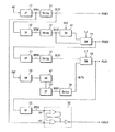
図2は、そのようなセンスアンプ制御回路の1実施形態を示す。ここで、図1のセンスアンプは、3つの制御信号PSAC1、PSAC2及びPSAC3を使用し、ラッチ回路11は、PLCHに応答し、このような全ての信号がセンスアンプ制御回路から発生すると仮定する。
図2を参照すると、マスタ信号MSは、短パルス発生器21に印加される。短パルス発生器21の出力は、遅延回路31を介してPSAC1に結合される。遅延回路31の出力は、短パルス発生器22に印加される。短パルス発生器22の出力は、シフトレジスタ41と選択スイッチ51とに印加される。シフトレジスタ41は、クロック信号CLKの各入力に応答して1クロックだけシフトされた信号を発生する。選択スイッチ51は、ラテンシ情報信号LIに応答してシフトレジスタ41の出力と遅延回路32の出力のうち、1つを交互に伝送してPSAC2を発生する。
【0012】
PSAC2は、また、短パルス発生器22の入力に接続される。短パルス発生器22の出力は、遅延回路33を介して選択スイッチ52の一方の入力端子に印加される。他方の入力端子には、ラテンシカウンタ(図示せず)の出力信号であるCNTが、スイッチ53、シフトレジスタ42、短パルス発生器24及び、遅延回路34を介して印加される。スイッチ53は、ラテンシカウンティング信号CNTをラテンシ情報信号LIに応答して伝送し、シフトレジスタ42は、CNTをCLKのクロッキングによって1クロックシフトされた信号に変換する。選択スイッチ52は、ラテンシ情報信号LIに応答して遅延回路32及び34の出力のうち、1つを交互に伝送してセンスアンプラッチ制御信号PLCHを発生する。PLCHは、また、ゲートラッチ回路60の一方の入力に印加される。ゲートラッチ回路60の他方の入力は短パルス発生器21の出力に接続されている。ゲートラッチ回路60の出力は、PSAC3になる。
【0013】
短パルス発生器に接続された遅延回路は、短パルス発生器によって形成された短パルスから延長されたパルス幅を有する信号を発生する。ラテンシカウンティング信号CNTは、1センシングサイクル中のクロックの数を示し、与えられた1サイクルのセンシング期間内でできるだけラッチ時点を遅延させることによってセンシング安定性を図るために提供される。図2の構成において、短パルス発生器を遅延回路及びスイッチの連結関係及びそれらの内部構成は、環境によって多用な形態で変更することができる。例えば、シフトレジスタの段数は、シフトされる出力信号のシフト幅を決定する。
【0014】
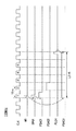
次に同期式メモリ装置の動作速度を決定する多様なクロック周波数によって制御信号の各々を発生する過程に関して説明する。
ここで、センスアンプの1センシングサイクル時間は約30nsと仮定する。まず、図3を参照すると、20MHz(この場合、1クロックサイクルが50nsであることを意味し、通常の非同期式メモリの場合と相異はない)程度の低周波数でPSAC1は、入力が短パルス発生器21を介してマスタ信号MSに接続される遅延回路31の出力から発生される。50nsのクロック周期は、30ns程度のセンシングサイクルに十分な時間であるために、PSAC2は、シフトレジスタ41を介さず、短パルス発生器22と遅延回路32とだけを介してPSAC1から発生される。
【0015】
ここで、ラテンシ情報LIは、1として、これはラテンシがないのと同一であるため、選択スイッチ51は、遅延回路32の出力をPSAC2に直接接続する。PSAC2の場合と同じように、PLCHは、PSAC2から短パルス発生器23と遅延回路33とからなる経路を介して発生される。選択スイッチ52も遅延回路33の出力をPLCHに接続し、CNTからの信号を切断する。短パルス発生器21の以前の出力によって高レベルのラッチ状態を維持していたPSAC3は、短パルス発生器25とラッチ回路60とを介して印加されるPLCHに応答して低レベルに降下する。
【0016】
図3に示すように、センスアンプラッチ信号PLCHは、ラテンシ情報を印加しなくてもクロック信号の1周期内で活性化される。
しかし、ラテンシが3に設定され、クロック周波数が66MHzの高帯域動作の場合を示す図4を参照すると、PSAC2は、PSAC1から短パルス発生器22、遅延回路32及びシフトレジスタ41を介して発生される。シフトレジスタ41は、遅延回路32の出力信号を図4に示すように右の方に1クロックシフトさせる。選択スイッチ51は、遅延回路32の出力をPSAC2に直接接続せず、シフトレジスタ41の出力をPSAC2に接続する。これは、選択スイッチ51に印加されるLIが、マスタ信号MSが活性化された後、3クロック以内にメモリセルアレイからのデータビットをセンスアンプラッチ回路の出力に伝送させるのに有効なラテンシ情報信号であるからである。
【0017】
図3の場合とは異なり、選択スイッチ52は、PSAC2からの経路ではなく、CNTからの経路を選択する。従って、PLCHは、スイッチ53、シフトレジスタ42、短パルス発生器24及び遅延回路34を介してCNTから発生し、センスアンプの活性化期間のうち、最後のクロック期間で活性化される。PSAC3によって設定されるセンスアンプの活性化期間は、ゲートラッチ回路60の入力端子62印加されるマスタ信号MSの活性化と共に始まり、PLCHに応答する短パルス発生器25の出力がゲートラッチ回路60の他の入力端子64に印加されるときに終了する。
【0018】
図5は、図4の場合よりさらに高いクロック周波数の場合を示しており、100MHzの動作周波数で、ラテンシが5の場合である。センスアンプの活性化期間がCLKの5クロックサイクルの間続く間に、PSAC1を除く制御信号PSAC2、PLCH及びPSAC3が、図4に示すように、現在のラテンシ情報信号によって制御される経路を介して発生する。
【0019】
低周波数の場合、図3に示す制御信号発生過程は、同期式メモリ装置においても、周知のATDに基づく非同期式制御技術と類似であることが分かる。しかし、クロックサイクルが同期式メモリ装置のセンスアンプのセンシング周期より短い場合においては、図4及び図5に示すように、所定のラテンシ情報の制御によりセンスアンプラッチ回路の制御信号は遅延させられ、センスアンプは有効なデータビットのための十分なセンシング時間を持つことが出来る。その結果、各クロック周波数に対応して設定されたラテンシ信号が完全なセンシング動作を実行することが出来るため同期式メモリ装置の収率が向上する。
【0020】
【発明の効果】
本発明では、一定の周期を有するクロック信号によってセンシング動作を制御することができる。また多様なクロック周波数に適応可能であるようにセンシング動作を制御することができる。さらに、クロック周波数環境に対応する所定のラテンシ情報によってセンシング動作を制御することができる。
【図面の簡単な説明】
【図1】同期式メモリでセンスアンプを制御する機能ブロックを示す。
【図2】同期式メモリでセンスアンプとセンスアンプラッチ回路とに印加される制御信号を発生するセンスアンプ制御回路の1実施形態を示す。
【図3】同期式メモリに印加されるシステムクロックの周波数が20MHzであるときに、図2に示すセンスアンプ制御回路から発生する信号の波形を示す。
【図4】同期式メモリに印加されるシステムクロックの周波数が66MHzであるときに、図2に示すセンスアンプ制御回路から発生する信号の波形を示す。
【図5】同期式メモリに印加されるシステムクロックの周波数が100MHzであるときに、図2に示すセンスアンプ制御回路から発生する信号の波形を示す。
【符号の説明】
1:メモリセルアレイ
3:行デコーダ
5:列デコーダ
7:列ゲート回路
9:センスアンプ
11:センスアンプラッチ回路
13:データバッファ
15:センスアンプ制御回路[0001]
BACKGROUND OF THE INVENTION
The present invention relates to a synchronous semiconductor memory device, and more particularly to a technique for controlling a sense amplifier used in a synchronous memory device that responds to an external clock signal.
[0002]
[Prior art]
The address transition detection circuit ATD is a semiconductor memory such as a read-only memory, and is used for controlling an internal access circuit such as a sense amplifier circuit at an appropriate control timing, and improves the sensing operation of stored data. The control signal is activated. The address transition detection circuit detects a change in the external address signal and generates a master signal notifying the address transition. All control signals used for the sensing operation in the memory device are formed by delaying the master signal or combining it with the master signal. Such an ATD-based control signal has a unique pulse width and a delay time between them, and is fixed at a constant value regardless of the external operating frequency, and is manufactured based on circuit design criteria. It cannot be changed later.
[0003]
[Problems to be solved by the invention]
In the sensing operation of the read-only memory, since one sensing cycle that defines the period from the start of the sensing operation to the storage of the sensing result is always constant, the sensing timing shift is caused by power supply noise or timing change. There is a possibility of storing wrong data regardless of the relationship or selecting a defective memory cell. Such a mismatch between the control signal and the sensing cycle time reduces the yield of the memory device. Furthermore, when the sensing time of the sense amplifier is required to be shorter than the design value, a newly changed address transition detection circuit is necessary.
[0004]
In order to increase the operating frequency of an asynchronous memory device, a synchronous memory is considered a useful technique for high-bandwidth memory operation. The synchronous memory performs an internal operation in response to a system clock having a predetermined pulse width and frequency. Since the system clock is assigned to one of several frequencies, the sense amplifier is controlled by the system clock. Must be designed to match one of the frequencies.
[0005]
Accordingly, a first object of the present invention is to provide a synchronous read-only memory device having a circuit for controlling a sensing operation by a clock signal having a certain period.
A second object is to provide a synchronous read-only memory device having a circuit for controlling a sensing operation so as to be adaptable to various clock frequencies.
A third object is to provide a synchronous read-only memory device having a circuit for controlling a sensing operation under various clock frequency conditions according to predetermined latency information corresponding to the clock frequency condition.
[0006]
[Means for Solving the Problems]
To achieve the above object, a synchronous read-only memory device according to the present invention is coupled to a clock signal source having a constant oscillation pulse period, a sense amplifier operated by a plurality of first control signals, and an output of the sense amplifier. And a circuit for generating a first control signal and a second control signal applied to the latch circuit in response to information corresponding to the pulse period of the clock signal.
[0007]
Further, the read-only memory of the present invention includes a clock signal source having a constant oscillation pulse period, a sense amplifier operated by a plurality of control signals, a latch circuit coupled to the output of the sense amplifier, a control signal, a latch And a latch control signal generated in response to latency information corresponding to the pulse period of the clock signal under a predetermined frequency condition. Is generated in response to a latency counting signal under a predetermined frequency condition. The generation circuit includes at least a selection switch that determines a delay state of the control signal in response to the latency information signal. The predetermined frequency condition is when one sensing cycle time of the sense amplifier is longer than the pulse period of the clock signal.
[0008]
The read-only memory according to the present invention includes a master signal source generated when an address signal changes, a clock signal source having a constant oscillation pulse period, a sense amplifier operated by a plurality of sense amplifier control signals, and a sense amplifier A latch circuit coupled to the output; a first circuit for generating a first control signal for the sense amplifier control signal; a second circuit for generating a second control signal for the sense amplifier control signal; and a latch applied to the latch circuit A third circuit for generating a control signal and a fourth circuit for generating a third control signal of the sense amplifier control signal, the second control signal corresponding to the pulse period of the clock signal under a predetermined frequency condition; The latch control signal is generated in response to the latency counting signal under the predetermined frequency condition, and the third control signal is generated in response to the latency information. Is activated in response to the master signal is inactivated in response to the latch control signal.
[0009]
DETAILED DESCRIPTION OF THE INVENTION
Hereinafter, embodiments of the present invention will be described with reference to the drawings. In addition, the same code | symbol is attached | subjected to the same part in drawing.
Referring to FIG. 1 showing a functional configuration for performing a sensing operation in synchronization with a system clock signal CLK in a synchronous memory device according to the present invention, a
[0010]
The master signal MS is supplied from an address transition detection circuit (not shown) that generates a short pulse when the address changes. The Latin information signal LI is a mode register that generates a signal that determines the number of clock cycles of CLK after the address strobe signal (eg, column address strobe signal) is activated until the first data bit appears at the output terminal. Supplied from Latin is provided to ensure stable data detection and reliable data values in a high bandwidth operating environment of a synchronous memory device. The Latin value is proportional to the operating frequency of the synchronous memory device. That is, the low frequency operation memory has a small latency value, and the high frequency operation memory has a large latency value. For example, when the frequency of the clock signal is about 20 MHz, a latency of one clock cycle is sufficient, but when the sensing cycle is 30 ns and the frequency of the clock signal is 100 MHz, three clock cycles or more Latency is required. Therefore, the sense
[0011]
FIG. 2 shows one embodiment of such a sense amplifier control circuit. Here, it is assumed that the sense amplifier of FIG. 1 uses three control signals PSAC1, PSAC2, and PSAC3, and that the
Referring to FIG. 2, the master signal MS is applied to the
[0012]
[0013]
A delay circuit connected to the short pulse generator generates a signal having a pulse width extended from the short pulse formed by the short pulse generator. The latin counting signal CNT indicates the number of clocks in one sensing cycle, and is provided for sensing stability by delaying the latch time as much as possible within a given sensing period of one cycle. In the configuration of FIG. 2, the connection relationship of the short pulse generator, the delay circuit and the switch, and the internal configuration thereof can be changed in various forms depending on the environment. For example, the number of stages of the shift register determines the shift width of the output signal to be shifted.
[0014]
Next, a process of generating each of the control signals with various clock frequencies that determine the operation speed of the synchronous memory device will be described.
Here, it is assumed that one sensing cycle time of the sense amplifier is about 30 ns. First, referring to FIG. 3, PSAC1 has a short pulse input at a low frequency of about 20 MHz (in this case, meaning that one clock cycle is 50 ns, which is not different from the case of a normal asynchronous memory). It is generated from the output of the
[0015]
Here, the latency information LI is 1, which is the same as no latency, so the
[0016]
As shown in FIG. 3, the sense amplifier latch signal PLCH is activated within one cycle of the clock signal without applying latency information.
However, referring to FIG. 4 showing the case of high-band operation with a latency set to 3 and a clock frequency of 66 MHz, PSAC2 is generated from PSAC1 via
[0017]
Unlike the case of FIG. 3, the
[0018]
FIG. 5 shows a case where the clock frequency is higher than the case of FIG. 4, where the latency is 5 at an operating frequency of 100 MHz. While the activation period of the sense amplifier continues for 5 clock cycles of CLK, the control signals PSAC2, PLCH and PSAC3 except for PSAC1 are passed through a path controlled by the current latency information signal as shown in FIG. appear.
[0019]
In the case of a low frequency, the control signal generation process shown in FIG. 3 is similar to the known asynchronous control technique based on ATD even in the synchronous memory device. However, when the clock cycle is shorter than the sensing cycle of the sense amplifier of the synchronous memory device, as shown in FIGS. 4 and 5, the control signal of the sense amplifier latch circuit is delayed by controlling the predetermined latency information. The sense amplifier can have sufficient sensing time for valid data bits. As a result, the latency signal set corresponding to each clock frequency can execute a complete sensing operation, thereby improving the yield of the synchronous memory device.
[0020]
【The invention's effect】
In the present invention, the sensing operation can be controlled by a clock signal having a certain period. In addition, the sensing operation can be controlled so as to be adaptable to various clock frequencies. Furthermore, the sensing operation can be controlled by predetermined latency information corresponding to the clock frequency environment.
[Brief description of the drawings]
FIG. 1 shows functional blocks for controlling a sense amplifier in a synchronous memory.
FIG. 2 shows an embodiment of a sense amplifier control circuit that generates a control signal applied to a sense amplifier and a sense amplifier latch circuit in a synchronous memory.
3 shows a waveform of a signal generated from the sense amplifier control circuit shown in FIG. 2 when the frequency of the system clock applied to the synchronous memory is 20 MHz.
4 shows a waveform of a signal generated from the sense amplifier control circuit shown in FIG. 2 when the frequency of the system clock applied to the synchronous memory is 66 MHz.
5 shows a waveform of a signal generated from the sense amplifier control circuit shown in FIG. 2 when the frequency of the system clock applied to the synchronous memory is 100 MHz.
[Explanation of symbols]
1: Memory cell array 3: Row decoder 5: Column decoder 7: Column gate circuit 9: Sense amplifier 11: Sense amplifier latch circuit 13: Data buffer 15: Sense amplifier control circuit
Claims (7)
一定の発振パルス周期を有するクロック信号源と、
複数のセンスアンプ制御信号によって動作するセンスアンプと、
前記センスアンプの出力に結合されたラッチ回路と、
センスアンプ制御回路とを備え、
前記センスアンプ制御回路は、
第1のセンスアンプ制御信号を発生する第1回路と、
所定の周波数条件下で、前記クロック信号のパルス周期に対応するラテンシ情報に応じて発生される第2のセンスアンプ制御信号を発生する第2回路と、
前記周波数条件下で、クロックサイクルが1センシングサイクルより短い場合においては、与えられた1サイクルのセンシング期間内でできるだけ、前記ラッチ回路が、前記センスアンプの出力データをラッチするタイミングを遅延させるように、1センシングサイクル中のクロックの数を示すラテンシカウント信号に応答してラッチ制御信号を発生し、該ラッチ制御信号を前記ラッチ回路に供給する第3回路と、
前記マスタ信号に応答してセンスアンプを活性化するために起動され、前記センスアンプの出力データをラッチするタイミングに応答してセンスアンプを非活性化するために停止される第3のセンスアンプ制御信号を発生する第4回路とを有することを特徴とする読出し専用メモリ装置。A master signal source that generates a master signal when the address changes;
A clock signal source having a constant oscillation pulse period;
A sense amplifier operated by a plurality of sense amplifier control signals;
A latch circuit coupled to the output of the sense amplifier;
A sense amplifier control circuit,
The sense amplifier control circuit includes:
A first circuit for generating a first sense amplifier control signal;
A second circuit for generating a second sense amplifier control signal generated according to latency information corresponding to a pulse period of the clock signal under a predetermined frequency condition;
When the clock cycle is shorter than one sensing cycle under the frequency condition, the latch circuit delays the timing of latching the output data of the sense amplifier as much as possible within a given sensing period. A third circuit for generating a latch control signal in response to a latency count signal indicating the number of clocks in one sensing cycle and supplying the latch control signal to the latch circuit;
Third sense amplifier control activated to activate a sense amplifier in response to the master signal and stopped to deactivate the sense amplifier in response to timing to latch output data of the sense amplifier And a fourth circuit for generating a signal.
前記第3のセンスアンプ制御信号のリードエッジに同期してセンシングサイクルを開始し、前記第3のセンスアンプ制御信号のトレールエッジに同期して前記センシングサイクルを終了するセンスアンプと、
前記センシングサイクルの期間に、前記センスアンプの出力から読出しデータを受信し、前記センスアンプラッチ制御信号に応答して前記読出しデータをラッチするセンスアンプラッチ回路とを有し、
前記第3センスアンプ制御信号は、前記マスタ信号のリードエッジに同期したリードエッジと前記センスアンプラッチ制御信号のトレールエッジに同期したトレールエッジとを有し、前記センスアンプラッチ制御信号は、クロックサイクルが1センシングサイクルより短い場合においては、与えられた1サイクルのセンシング期間内でできるだけセンスアンプの出力データをラッチするタイミングを遅延させるように、1センシングサイクル中のクロックの数を示すラテンシカウント信号に応答して発生されることを特徴とする集積回路メモリデバイス。A first circuit that generates a first sense amplifier control signal in response to a master signal, a second circuit that generates a second sense amplifier control signal in response to the master signal and latency information, a latency counting signal, and latency information sense amplifier control comprising Doo third circuit for generating a sense amplifier latch control signal in response to, and a fourth circuit for generating a third sense amplifier control signal in response to the sense amplifier latch signal and the master signal Circuit,
A sense amplifier that starts a sensing cycle in synchronization with a lead edge of the third sense amplifier control signal, and ends the sensing cycle in synchronization with a trail edge of the third sense amplifier control signal;
A sense amplifier latch circuit that receives read data from the output of the sense amplifier during the sensing cycle and latches the read data in response to the sense amplifier latch control signal;
Said third sense amplifier control signal, possess a trail edge which is synchronized said master signal synchronized with lead edge to the lead edge of the the trail edge of the sense amplifier latch control signal, the sense amplifier latch control signal, clock cycle Is shorter than one sensing cycle, a latency count signal indicating the number of clocks in one sensing cycle so as to delay the timing of latching the output data of the sense amplifier as much as possible within a given sensing period. An integrated circuit memory device generated in response to
Applications Claiming Priority (2)
| Application Number | Priority Date | Filing Date | Title |
|---|---|---|---|
| KR1019980030050A KR100301367B1 (en) | 1998-07-25 | 1998-07-25 | Synchronous Semiconductor Memory Device with Sense Amplifier Control |
| KR1998P-30050 | 1998-07-25 |
Publications (2)
| Publication Number | Publication Date |
|---|---|
| JP2000048588A JP2000048588A (en) | 2000-02-18 |
| JP3832548B2 true JP3832548B2 (en) | 2006-10-11 |
Family
ID=19545209
Family Applications (1)
| Application Number | Title | Priority Date | Filing Date |
|---|---|---|---|
| JP21098699A Expired - Fee Related JP3832548B2 (en) | 1998-07-25 | 1999-07-26 | Read-only memory device |
Country Status (4)
| Country | Link |
|---|---|
| US (1) | US6226222B1 (en) |
| JP (1) | JP3832548B2 (en) |
| KR (1) | KR100301367B1 (en) |
| TW (1) | TW530309B (en) |
Families Citing this family (6)
| Publication number | Priority date | Publication date | Assignee | Title |
|---|---|---|---|---|
| KR100424118B1 (en) | 2001-05-03 | 2004-03-24 | 주식회사 하이닉스반도체 | Synchronous semiconductor memory device for controlling cell operation using frequency informations of clock signal |
| US7123530B2 (en) * | 2003-10-09 | 2006-10-17 | Micron Technology, Inc. | AC sensing for a resistive memory |
| US7134034B1 (en) * | 2003-10-15 | 2006-11-07 | Integrated Device Technology, Inc. | Data paths with receiver timing fixable to a downstream stage and methods of operation thereof |
| JP4683617B2 (en) * | 2005-01-27 | 2011-05-18 | ルネサスエレクトロニクス株式会社 | Microcomputer and microcomputer optimization method |
| KR100735011B1 (en) * | 2006-01-23 | 2007-07-03 | 삼성전자주식회사 | NOR flash memory and its reading method |
| KR100927404B1 (en) * | 2008-02-29 | 2009-11-19 | 주식회사 하이닉스반도체 | Lead Mask Test Circuit and Control Method |
Family Cites Families (3)
| Publication number | Priority date | Publication date | Assignee | Title |
|---|---|---|---|---|
| KR0147706B1 (en) * | 1995-06-30 | 1998-09-15 | 김주용 | Fast synchronous mask rom |
| KR100274591B1 (en) * | 1997-07-29 | 2001-01-15 | 윤종용 | Synchronous Burst Mask and Its Data-Reading Method |
| US5978284A (en) * | 1997-08-22 | 1999-11-02 | Micron Technology, Inc. | Synchronous memory with programmable read latency |
-
1998
- 1998-07-25 KR KR1019980030050A patent/KR100301367B1/en not_active Expired - Fee Related
-
1999
- 1999-07-22 US US09/359,217 patent/US6226222B1/en not_active Expired - Fee Related
- 1999-07-22 TW TW088112432A patent/TW530309B/en not_active IP Right Cessation
- 1999-07-26 JP JP21098699A patent/JP3832548B2/en not_active Expired - Fee Related
Also Published As
| Publication number | Publication date |
|---|---|
| JP2000048588A (en) | 2000-02-18 |
| US6226222B1 (en) | 2001-05-01 |
| KR100301367B1 (en) | 2001-10-27 |
| KR20000009548A (en) | 2000-02-15 |
| TW530309B (en) | 2003-05-01 |
Similar Documents
| Publication | Publication Date | Title |
|---|---|---|
| US8004911B2 (en) | Memory system, memory device, and output data strobe signal generating method | |
| KR100822001B1 (en) | Method of Operating Semiconductor Memory and Semiconductor Memory Circuit | |
| US7215588B2 (en) | Apparatus for controlling self-refresh period in memory device | |
| KR100303775B1 (en) | Method and apparatus for controlling data strobe signal in DISD DRAM | |
| KR100522433B1 (en) | Domain crossing circuit | |
| US6198327B1 (en) | Pulse generator with improved high speed performance for generating a constant pulse width | |
| KR100622841B1 (en) | Method and apparatus for controlling data rate of clocking circuit | |
| KR100311044B1 (en) | Latency determination circuit capable of adjusting latency number according to clock frequency and method of determining of latency thereof | |
| US6809983B2 (en) | Clock generator for pseudo dual port memory | |
| JP2003283322A (en) | Interface circuit and semiconductor device | |
| US6252820B1 (en) | Semiconductor memory device capable of monitoring and adjusting the timing and pulse width of internal control signals | |
| US6320818B1 (en) | Semiconductor storage device, and method for generating timing of signal for activating internal circuit thereof | |
| JP3832548B2 (en) | Read-only memory device | |
| KR20010045596A (en) | Synchronous mask rom devicve which supports a consecutive read operation | |
| JP2004273008A (en) | Clock synchronization type semiconductor storage device | |
| US6606272B2 (en) | Method and circuit for processing output data in pipelined circuits | |
| CN101071625B (en) | Method and system for preventing noise interference in high speed low power memory | |
| JPH11176161A (en) | Synchronous semiconductor memory device and data output method | |
| CN117311598B (en) | Synchronous input buffer control using write shifter | |
| KR100389038B1 (en) | Synchronous sram device with late write function | |
| US6674666B2 (en) | Device and method for timing the reading of a nonvolatile memory with reduced switching noise | |
| US6643217B2 (en) | Semiconductor memory device permitting early detection of defective test data | |
| JPH09180443A (en) | Semiconductor memory circuit | |
| KR100670694B1 (en) | Output enable signal generator of high speed memory device | |
| EP1122733A1 (en) | Internal regeneration of the address latch enable (ALE) signal of a protocol of management of a burst interleaved memory and relative circuit |
Legal Events
| Date | Code | Title | Description |
|---|---|---|---|
| A977 | Report on retrieval |
Free format text: JAPANESE INTERMEDIATE CODE: A971007 Effective date: 20050620 |
|
| A131 | Notification of reasons for refusal |
Free format text: JAPANESE INTERMEDIATE CODE: A131 Effective date: 20050705 |
|
| A521 | Request for written amendment filed |
Free format text: JAPANESE INTERMEDIATE CODE: A523 Effective date: 20050930 |
|
| A02 | Decision of refusal |
Free format text: JAPANESE INTERMEDIATE CODE: A02 Effective date: 20060221 |
|
| A521 | Request for written amendment filed |
Free format text: JAPANESE INTERMEDIATE CODE: A523 Effective date: 20060427 |
|
| A911 | Transfer to examiner for re-examination before appeal (zenchi) |
Free format text: JAPANESE INTERMEDIATE CODE: A911 Effective date: 20060502 |
|
| A131 | Notification of reasons for refusal |
Free format text: JAPANESE INTERMEDIATE CODE: A131 Effective date: 20060530 |
|
| A521 | Request for written amendment filed |
Free format text: JAPANESE INTERMEDIATE CODE: A523 Effective date: 20060601 |
|
| TRDD | Decision of grant or rejection written | ||
| A01 | Written decision to grant a patent or to grant a registration (utility model) |
Free format text: JAPANESE INTERMEDIATE CODE: A01 Effective date: 20060627 |
|
| A61 | First payment of annual fees (during grant procedure) |
Free format text: JAPANESE INTERMEDIATE CODE: A61 Effective date: 20060711 |
|
| R150 | Certificate of patent or registration of utility model |
Free format text: JAPANESE INTERMEDIATE CODE: R150 |
|
| LAPS | Cancellation because of no payment of annual fees |